
 Open Access Article
 This Open Access Article is licensed under a
 Creative Commons Attribution 3.0 Unported Licence
Selective gas phase pulsed etching of oxides with NbCl5
Juha
Ojala
 *,
Marko
Vehkamäki
,
Mykhailo
Chundak
,
Anton
Vihervaara
,
Kenichiro
Mizohata
and
Mikko
Ritala
*
*,
Marko
Vehkamäki
,
Mykhailo
Chundak
,
Anton
Vihervaara
,
Kenichiro
Mizohata
and
Mikko
Ritala
*
Department of Chemistry, University of Helsinki, FI-00014 Helsinki, Finland. E-mail: juha.t.ojala@helsinki.fi; mikko.ritala@helsinki.fi
First published on 9th December 2024
Abstract
Ta2O5 films were etched with NbCl5 using a chemical vapor etching method known as gas-phase pulsed etching (GPPE) where the etchant is delivered in short pulses with inert gas purging in between the pulses. Arrhenius type dependence of etch per cycle (EPC) on temperature was found at 275–375 °C and the activation energy of the etching reaction is estimated at 120 kJ mol−1. Length of the etchant pulse had a linear effect on EPC and increasing the purge length also increased EPC. Roughnesses of the partially etched films increased from 0.2 to 1.4 nm, as measured by atomic force microscopy. No residual Nb or Cl was detected in the films by energy-dispersive X-ray spectroscopy, but a small amount of Cl residue was seen with in vacuo X-ray photoelectron spectroscopy. Etching of TiO2 and ZrO2 was also observed but HfO2 was not etched by NbCl5 at 300–400 °C. Selectivity with respect of SiO2, Al2O3, and TiN was also proven at the same temperature range. EPC up to 2.8, 1.1, and 4.0 Å were observed for Ta2O5, ZrO2, and TiO2, respectively.
1. Introduction
Ta2O5 is a high-k oxide that has been studied as an etch mask for silicon,1 as a dielectric layer in dynamic and resistive random access memories,2,3 metal-oxide–semiconductor field effect transistors,4 and many other applications. Hafnium-based dielectric materials are used on an industrial scale as gate dielectrics in complementary metal-oxide semiconductor transistors, and ZrO2 and TiO2 have also been considered as alternative high-k materials.5 ZrO2 is specifically used as a dielectric in dynamic random access memory.6 As these materials are increasingly used in 3D structures such as gate-all-around transistors and 3D memory stacks, processes used to deposit and etch these materials need to operate isotropically, without a line of sight to the surface. In addition, etching needs to be selective to a given material.Although plasma etching is well-known for the anisotropic reactive ion etching (RIE), it can also be used for isotropic etching.7 Operation in remote plasma mode can provide fully isotropic etching as only a flux of neutral radicals is reaching the substrate. This also decreases plasma-induced damage to the substrate as it does not come into a direct contact with the plasma. However, plasma methods require careful control to maintain selectivity and can suffer from poor conformality due to recombination of the radical species. Chemical vapor etching (CVE) is a gentler approach, where gas phase etchants react with the substrate to form volatile compounds. The thermally activated reactions offer more selectivity through chemistry, and the etchant gas is inherently more stable than the transient radical species from plasma.
CVE methods have been developed for etching Si and SiO2, as well as other oxides. These most often rely on using volatile fluorine compounds such as XeF2 and HF to produce volatile fluorides as etch products.8–10 These continuous etching methods can be modified to a cyclic etching process known as gas-phase pulsed etching (GPPE).11,12 Here the etchant gas or vapor pulses are separated by inert gas purging periods, during which volatile etch products can be removed more efficiently. In GPPE the etch depth can be simply controlled by the number of etch cycles. The etch per cycle (EPC) is controlled by varying process parameters such as reactor temperature, etchant pulse and purge times, and partial pressure of the etchant.
Ta2O5 has previously been etched using TaCl5 and an unspecified oxygen containing precursor, according to a patent by Dautartas and Sneh.13 Etching of Ta2O5 by TaCl5 has also been observed during atomic layer deposition (ALD) of Ta2O5 with TaCl5 and H2O.14 When a corresponding Nb2O5 ALD process with NbCl5 and H2O was attempted it was seen that Nb2O5 was etched even more aggressively with NbCl5.15 Mechanistic studies16 verified that the etching occurred according to the reaction:
| 3 NbCl5 (g) + Nb2O5 (s) → 5 NbOCl3 (g) | (1) |
Because of the chemical similarity of tantalum and niobium it is presumed that NbCl5 etches Ta2O5 as well. Compared to TaCl5, NbCl5 has the advantage of being more abundant and affordable, although both tantalum and niobium are considered critical elements.
Several dry etching processes using plasma have been demonstrated for the group 4 oxides TiO2, ZrO2 and HfO2,17–19 but their selectivity is limited. Chemical vapor etching of TiO2 has been demonstrated using HF and WF6.20,21 In the latter case, diffusion of fluorine into the subsurface TiO2 layers was noticed. ZrO2 and HfO2 have been previously etched using atomic layer etching,22,23 but few continuous CVE methods for these oxides have been published.
This study introduces NbCl5 as a new etchant for GPPE of Ta2O5, TiO2, and ZrO2, with excellent selectivity to SiO2, Al2O3, TiN, and HfO2.
2. Experimental
Ta2O5, Al2O3, TiO2, ZrO2, and HfO2 films used in the etching experiments were grown by atomic layer deposition on Si(100) in an F-120 ALD reactor (ASM Microchemistry Oy). Deionized water delivered from an external source was used as the oxygen precursor for the oxide film deposition. The metal precursors and deposition parameters are presented in Table 1. The metal precursors evaporated at room temperature were delivered from external sources with vacuum draw and the others were sublimed from glass boats inside the reactor. SiO2 films were grown by oxidizing silicon wafers in air at 950 °C for 80 minutes. TiN films were received from a collaborating company. Measured film properties are shown in Table 2.| Film | Metal precursor | Precursor temperature (°C) | Deposition temperature (°C) |
|---|---|---|---|
| Ta2O5 | Tantalum ethoxide, Ta(OEt)5 | 95 | 325 |
| TiO2 | Titanium tetrachloride, TiCl4 | RT | 150, 300 |
| ZrO2 | Tetrakis(ethylmethylamido)zirconium, Zr(NEtMe)4 (TEMAZr) | 90 | 250 |
| HfO2 | Tetrakis(ethylmethylamido)hafnium, Hf(NEtMe)4 (TEMAHf) | 40 | 250 |
| Al2O3 | Trimethylaluminum, AlMe3 (TMA) | RT | 200 |
| Material | Crystal phase | Refractive index | Density (g cm−3) | Impurity contents (at-%) | |||||
|---|---|---|---|---|---|---|---|---|---|
| C | N | H | Cl | O | Hf | ||||
| Ta2O5 | Amorphous | 2.21 | 8.04 | 0.1 | — | 0.2 | — | — | — |
| Al2O3 | Amorphous | 1.64 | 3.00 | 0.2 | — | 1.4 | — | — | — |
| TiO2 (300 °C) | Anatase | 2.51 | 3.77 | 0.1 | — | 0.1 | — | — | — |
| TiO2 (150 °C) | Amorphous | 2.40 | 3.85 | 0.1 | — | 0.2 | 0.5 | — | — |
| ZrO2 | Cubic | 2.11 | 5.63 | 0.9 | 0.4 | 1.5 | — | — | 0.5 |
| HfO2 | Monoclinic | 2.09 | 9.66 | 0.3 | 0.2 | 1.1 | — | — | — |
| TiN | Cubic | — | 5.09 | — | — | 0.8 | 0.6 | 9.2 | — |
Etching experiments were conducted in the F-120 reactor with NbCl5 (>99%, Strem Chemicals, Inc.) sublimed from a glass boat at 80 °C. The etchant was delivered to the sample in pulses followed by purge periods during which only N2 was flowing over the substrate. Ta2O5 films deposited on 5 × 5 cm2 silicon substrates were used for the etching experiments and 1 × 5 cm2 coupons cleaved from larger pieces were used for studying the selectivity. As the sample cassette can house two 5 × 5 cm2 substrates, native oxide covered silicon was used as the other substrate.
Film crystallinity was evaluated using a PANalytical X’Pert Pro MPD X-ray diffractometer with Cu Kα (λ = 1.54 Å) radiation and grazing incidence geometry. The same instrument was used for X-ray reflectivity (XRR) measurements.
Thicknesses of the films before and after etching were studied using ellipsometry (Filmsense FS-1 multi-wavelength ellipsometer with 465, 525, 590 and 635 nm wavelengths) and verified with XRR when possible. Ellipsometry measurements were taken from nine points on the sample in a 3 × 3 grid pattern. The etched thicknesses were calculated as a difference of film thicknesses before and after etching.
Atomic force microscopy (AFM, Veeco Multimode V instrument) was used to study roughnesses of the films. A Si probe with a nominal tip radius of 10 nm and a spring constant of 40 N m−1 was used to capture images in air. Roughness was calculated as a root-mean-square value (Rq) from the flattened images. Flattening was performed to remove artefacts from the sample tilt and scanner bow.
Energy dispersive X-ray spectrometer (EDS, Oxford INCA 350) connected to a Hitachi S-4800 field-emission scanning electron microscope (FE-SEM) was used to study compositions of the etched films. Film compositions before etching were measured using ToF-ERDA with a 35 MeV 127I-beam.
Elemental composition of the surface before and after etching was measured with X-ray photoelectron spectroscopy (XPS, PREVAC) with a monochromated Al Kα anode with a photon energy hν = 1486.7 eV as an X-ray source, a hemispherical electron analyzer and a 2D spatial detector. For survey spectra 2.5 × 25 mm slit was used and for detail scan measurements a 0.8 × 25 mm slit with electron pass energy of 100 eV. The latter allows to acquire the FWHM 0.61 eV for the Ag 3d as a reference. During the measurements the vacuum level was 3 × 10⁻¹⁰ mbar. Some experiments were done in vacuo in a vacuum cluster with an ALD reactor directly connected to the XPS. Detailed description of the system has been published elsewhere.24
Etching mechanism was studied using a modified F-120 reactor equipped with a Maxtek TM-400 quartz crystal microbalance (QCM) and Hiden HAL/3F 501 RC quadrupole mass spectrometer (QMS).25 Mass spectra of NbCl5 and etch products of Ta2O5 were measured by scanning the mass range of interest multiple times. During one scan the NbCl5 etchant was supplied. The scans without the NbCl5 supply were averaged and taken as a background that was subtracted from the mass spectrum measured during the NbCl5 supply.
Thermodynamic calculations were carried out using HSC chemistry 7.11 software (Outotec). Equilibrium concentrations were calculated at 10 mbar pressure with the following starting materials: 5 kmol N2 (g), 0.1 kmol NbCl5 (g), and 0.01 kmol Ta2O5.
An FEI Quanta 3D 200i FIB-SEM was used to prepare test specimens for selective etching. A 30 kV/100 pA gallium ion beam was used with 38° ion-to-surface incident angle, thus lowering the extent and depth of gallium implantation and increasing milling rate. The same FIB-SEM system was used for preparing cross-section specimens with normal lift-out procedures. The Hitachi S-4800 FE-SEM was used for imaging the patterned structures and the lift-out specimens. As the patterned oxide film stacks are insulating, sputtered Au/Pd films were used to assist both SEM imaging and FIB lift-out sample preparation.
3. Results
3.1. Thermodynamic calculations
Thermodynamics of etching Ta2O5 with NbCl5 were studied by calculating equilibrium concentrations at the temperature range of 0–400 °C (Fig. 1). Even though the real system is not in equilibrium during the etching, the equilibrium concentrations give an indication of the reaction products. Excess NbCl5 was used compared to Ta2O5 to approximate the etching conditions. The amount of the etchant compared to N2 and the total pressure of the system (10 mbar as in the experiments) corresponds approximately to the vapor pressure of NbCl5, 0.8 mbar. | ||
| Fig. 1 Equilibrium amounts of different chemical species in the reaction of 0.1 kmol NbCl5 and 0.01 kmol Ta2O5 calculated with HSC chemistry 7.11. | ||
According to the calculations no Ta2O5 remains in the system under the equilibrium and even the solid TaO2Cl is a very minor component (outside the graph range). At the low temperatures tantalum exists mostly as solid TaOCl3 and TaCl5, but above about 100 °C it is seen mainly as gaseous TaCl5. Gaseous TaOCl3 is also seen in low concentrations above 300 °C. Because there is an excess of NbCl5 in the input, it is also the dominant Nb species for most of the temperature range. The most abundant reaction product below 300 °C is solid NbO2Cl, with a minor component of solid NbOCl3. Above 300 °C gaseous NbOCl3 becomes the most abundant reaction product. This corresponds well to the observed etching onset temperature of 275 °C. The complete absence of Ta2O5 shows that it should always react with NbCl5. The dominant species indicate that tantalum preferentially binds with chlorine, forming TaCl5, and oxygen is removed as NbOCl3 according to the reaction:
| Ta2O5 (s) + 5 NbCl5 (g) → 2 TaCl5 (g) + 5 NbOCl3 (g) | (2) |
The Gibbs free energy changes for the reaction of NbCl5 (g) and Ta2O5 to produce either TaCl5 (g) or TaOCl3 (g), along with etching reactions for Al2O3, SiO2, TiO2, ZrO2, and HfO2 are presented in Fig. 2. Reaction R2 that produces TaCl5 is indeed thermodynamically much more favorable than reaction R3 that produces TaOCl3. For the reaction R2, the Gibbs free energy change becomes negative above about 325 °C. It is also seen that etching of ZrO2 and HfO2 become favorable at similar temperatures, and etching of TiO2 already at about 125 °C. On the other hand, etching of SiO2 and Al2O3 do not become favorable below 500 °C.
 | ||
| Fig. 2 Gibbs free energy changes for etching reactions of Nb2O5, Ta2O5, Al2O3, HfO2, ZrO2, SiO2, and TiO2 at the temperature range of 0–700 °C. | ||
Equilibrium concentrations were also calculated for the etching of ZrO2 and HfO2. They formed very similar compounds at high temperatures, with MCl4 (g) as the dominant species above 150 °C (M = Zr or Hf). Below this temperature there were slight differences: zirconium formed mostly solid ZrCl4, whereas hafnium was seen as solid HfOCl2 below 50 °C and solid HfCl4 at 50–150 °C. These temperatures are far from the observed etching temperatures, but the results indicate some difference between zirconium and hafnium, which are generally very similar in their chemistry.
3.2. Etching of Ta2O5
Effects of the pulsing parameters on the etch per cycle (EPC) were studied at 325 °C and the results from the center of the substate are presented in Fig. 3. The length of the etchant pulse had a linear effect on EPC, which indicates constant etch rate per time unit: 0.32 Å s−1. Etching with a continuous flow of NbCl5 without pulsing gave a similar etch rate of 0.30 Å s−1. The length of the purging period also had a significant effect on the EPC: increasing the purge length to 3 s increased the EPC from 0.25 Å to 0.42 Å (Fig. 3b). Sharma et al. saw a similar trend in GPPE of TiN with SOCl2 and attributed the increase of EPC with the increasing purge length to a better recovery of the etchant pressure in the source and better removal of less volatile etch products during the extended purge.11 The constant level reached in EPC with longer purge lengths can be attributed to the saturation of the etchant vapor in the source. The thermodynamic calculations indicate that etching of Ta2O5 proceeds via volatile TaCl5 so the extended purge might drive the etching by removing the volatile products from the reactor. A cycle of 1 s NbCl5 pulse and 3 s purge was chosen for the rest of the experiments.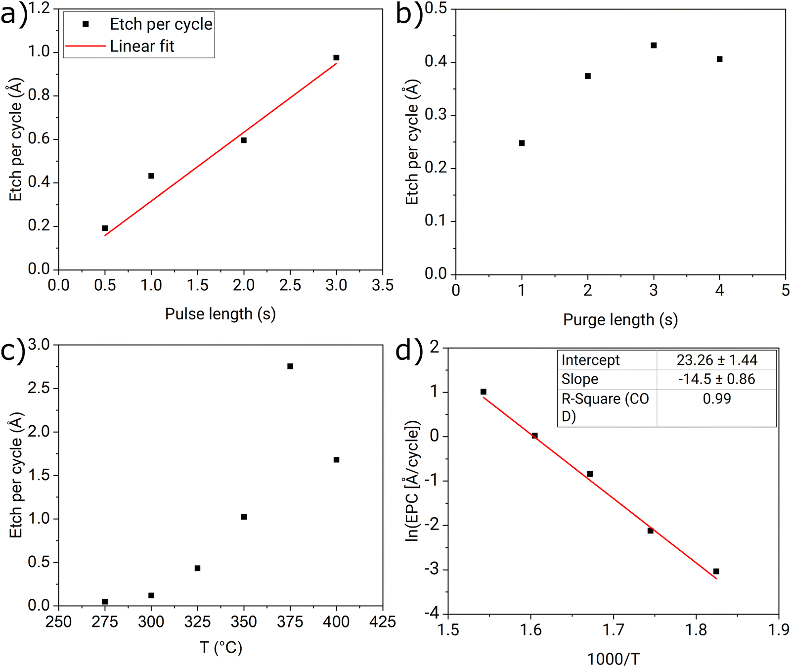 | ||
| Fig. 3 Dependence of EPC at 325 °C on (a) pulse length when the purge length was 3 s, and (b) purge length with 1 s pulses. (c) EPC as a function of the etching temperature, and (d) Arrhenius plot of EPC. Etching cycles consisted of 1 s etchant pulse followed by 3 s purge period and the number of cycles was varied from 100 to 1000 depending on the temperature. | ||
The effect of the etching temperature was studied next. Fig. 3c shows the EPC at the temperature range of 275–400 °C. Fig. 3d shows an Arrhenius plot of the same results, that is a natural logarithm of EPC plotted against the inverse of the etching temperature. It can be seen that the process follows the Arrhenius type dependence at the temperature range of 275–375 °C, and an activation energy of 120 kJ mol−1 was estimated from the slope of a linear fit. Above 375 °C, the EPC begins to diminish: 1.68 Å per cycle at 400 °C vs. 2.75 Å per cycle at 375 °C. The reason could be that at high temperatures NbCl5 is lost to side reactions or does not adsorb on the surface long enough for the reaction to take place.
The effect of the etchant load in the source boat was also studied (Fig. 4), and it was found that the EPC increases linearly with the mass of NbCl5 loaded for the experiment until around 300 mg. The etchant did not run out in any of the experiments, so the increase of EPC is likely due to a faster regeneration of the etchant vapor in the source. Most of the experiments up to this point had been done using a 200 mg etchant load and this was kept constant to ensure that the results are comparable.
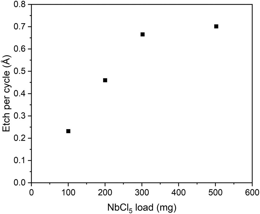 | ||
| Fig. 4 Effect of NbCl5 loading on EPC at 325 °C using 500 cycles of 1 s etchant pulses followed by 3 s purges. | ||
The reactor used in this study is of the cross-flow type. There was some profile in the etched thickness along the gas flow direction. The EPC was 2–14% higher at the etchant inlet side 1 cm from the substrate edge, and 6–17% lower at the exhaust side as compared to the center of the substrate. As the EPC follows Arrhenius dependence, the etch rate is reaction controlled and the profile is probably a result of the etchant being used up along the flow across the substrate. The etchant load did not have a significant effect on the profile, however. In shower-head and other top-flow reactors better uniformity is expected than in the cross-flow reactor used in this study.
Linearity of the etching was also studied with a series of 250–1140 etch cycles (Fig. 5). It is seen that the etch thickness follows the number of cycles linearly.
 | ||
| Fig. 5 Etch thickness as a function of the number of etch cycles at 325 °C. Cycles of 1 s NbCl5 pulse and 3 s purge with 200 mg NbCl5 loading. | ||
3.3. Film characterization
The films were amorphous according to XRD and no peaks were detected after partial etching either. After partial etching of the Ta2O5 films, elemental analysis with EDS detected only Ta, O, and C in the films, the last one being likely from atmospheric contamination. No Nb or Cl was detected with EDS. Measurements of the films with XPS after transferring the sample in vacuo from the reactor also showed Ta, O and C before etching, and a slight Cl residue after an etchant pulse. No Nb was detected in any of the samples. After complete etching of a Ta2O5 film at 325 °C, no Nb or Ta could be detected on the substrate with EDS. XPS did not show obvious peaks other than Si and O but a very small bump could be seen in the Ta 4f peak region, indicating trace amounts of tantalum left on the surface.Roughnesses of the partially etched films were studied with AFM (Fig. 6), which showed a slight increase from around 0.2 nm Rq for the unetched film to 1.4 nm when 30 nm of the film was etched. Beyond that the roughness of the films remained constant. The roughness might be caused by surface restructuring during the etching or by inherent stochastic effects of continuous etching. Another possibility is that the films had some small slower-etching crystalline domains which were too small to be detected with XRD.
 | ||
| Fig. 6 AFM images of (a) an unetched 44 nm thick Ta2O5 film and (b) a film after etching away 30 nm of Ta2O5. (c) Roughnesses of the films etched to various depths at 325 °C as measured by AFM. | ||
3.4. Mechanistic studies
To study the etching mechanism, Ta2O5 was deposited and etched in situ using a modified F-120 reactor equipped with QMS and QCM, which has been described in detail elsewhere.25 The mass spectrum of NbCl5 was measured prior to Ta2O5 deposition and the observed peaks are presented in Table 3 along with the fragments they are attributed to. The signals of HCl and NbOCl3 fragments are attributed to reactions with residual water in the reactor. The relative intensities of the species with the same number of Cl atoms corresponded to the natural abundances of 35Cl and 37Cl.| m/z | Fragment |
|---|---|
| 36 | [H35Cl]+ |
| 38 | [H37Cl]+ |
| 178/179 | [NbO35Cl2]+ |
| 181 | [NbO35Cl37Cl]+ |
| 214 | [NbO35Cl3]+ |
| 216 | [NbO35Cl237Cl]+ |
| 218 | [NbO35Cl37Cl2]+ |
| 233 | [Nb35Cl4]+ |
| 235 | [Nb35Cl337Cl]+ |
| 237 | [Nb35Cl237Cl2]+ |
Mass spectrum measured during the etching showed quite weak signals but the most significant etch products were identified as [TaCl4]+ species, a fragment of TaCl5, whereas TaOCl3 and its fragments did not significantly exceed the background. Different m/z values corresponding to the etchant and etch products were monitored as a function of time during the etchant pulsing (Fig. 7). The masses 235 and 216, corresponding to [NbCl4]+ and [NbOCl3]+ respectively, show clear signals during the etchant pulses, as does m/z 323, which corresponds to [TaCl4]+. On the other hand, m/z 302 [TaOCl3]+ does not deviate from the background. This observation supports that TaCl5, rather than TaOCl3, is the primary etch product. It can also be seen that the first few etchant pulses register weaker in the QMS. This is probably due to the first pulse being mostly consumed in reactions with the hydroxyl terminated surfaces left after the deposition of Ta2O5.
 | ||
| Fig. 7 QMS of NbCl5 fragments and etch products of Ta2O5 during etching at 325 °C. | ||
3.5. Etch selectivity
The selectivity of NbCl5 as an etchant was studied with thermal SiO2 and ALD grown Al2O3, TiO2, ZrO2, HfO2 and TiN films. Both crystalline and amorphous TiO2 films were studied. The Al2O3 films were amorphous and the ZrO2, HfO2, and TiN films were crystalline according to the XRD measurements. Etch rates at different temperature are presented in Fig. 8. | ||
| Fig. 8 EPC of selected materials with NbCl5 at different etching temperatures using 1 s pulses and 3 s purges. Error bars were calculated based on an estimated error of 1 nm for each thickness measurement due to inherent measurement error and variation in the measurement location and minor film thickness variation. | ||
It was observed that SiO2, Al2O3, and TiN were not etched to any significant degree. Some blistering of Al2O3 was observed at 350 and 400 °C (Fig. 9). Blistering of ALD Al2O3 films on silicon upon annealing has been observed previously in the literature. It is generally attributed to accumulation of hydrogen gas and/or water vapor at the interface as thick Al2O3 films act as diffusion barriers.26–28 The origin of water in our Al2O3 films is dehydroxylation of hydroxyl impurities.29 The EPC of ZrO2 was very low at 300 °C, but increased with the etching temperature and reached 1.1 Å at 400 °C. The EPC of HfO2, on the other hand, was negligible throughout the temperature range of 300–400 °C. No niobium residue was detected with EDS in any of the films after partial etching, and no zirconium or niobium were detected on the substrate after complete etching of a ZrO2 film at 400 °C.
 | ||
| Fig. 9 SEM image of Al2O3 film after exposure to NbCl5 at 350 °C. | ||
The selectivity between ZrO2 and HfO2 is unexpected as these materials share many similar properties, and the thermodynamics of their etching reactions are almost identical (Fig. 2). On the other hand, previous studies on ALE of ZrO2 and HfO2 have also found significantly different etch rates for these materials.22,30 Crystalline HfO2 films especially are generally harder to etch than crystalline ZrO2 films. These ALE processes were based on fluorination of the oxides followed by a ligand exchange with a chlorine containing compound. Lii-Rosales et al. studied the ligand exchange and onset temperatures of spontaneous etching of ZrF4 and HfF4 with SiCl2(CH3)2, SiCl(CH3)2H, and SiCl4. They found that the temperatures were consistently higher for HfF4, but this was not commented on in any way.31 Mullins et al. conducted density-functional theory studies on the fluorination of ZrO2 and HfO2 surfaces with HF, looking also for the temperature at which spontaneous etching of the oxide becomes preferable to the self-limiting reaction.32 They found that the minimum energy for the spontaneous etching diminished with increasing temperature and this effect was faster for ZrO2 than for HfO2, resulting in a lower etching temperature for ZrO2.
A patent by Horace Chandler33 describes removal of HfCl4 from ZrCl4 by passing a mixture of these metal chloride vapors through a mixture of HfO2 and ZrO2 powders, upon which HfCl4 preferentially reacts with ZrO2 to form HfO2 and ZrCl4. In our thermodynamic equilibrium calculations, HfO2 reacting with NbCl5 formed a significant fraction of HfOCl2 at low temperatures. ZrO2, on the other hand, formed mostly ZrCl4 with negligible amounts of ZrOCl2. These observations imply that hafnium has a stronger preference for binding to oxygen over chlorine as compared with zirconium.
Complete etching of both amorphous and crystalline TiO2 was possible, but it was found that the etching was very nonuniform and showed a counterintuitive profile where the film was etched slower at the side of the etchant inlet. Additionally, the films were significantly roughened or otherwise modified upon etching, and the same ellipsometry model could not be used to model the films before and after etching. Thus, determination of EPC was unreliable, but it could be seen to reach approximately 4 Å at 325 °C for crystalline TiO2 (Fig. 10). The films were investigated with EDS, but no niobium or other residues could be detected. No titanium or niobium could be detected on the substrate after complete etching.
 | ||
| Fig. 10 Approximate EPC of crystalline TiO2 films in the center of the substrate when etched with (1/3) s cycles of NbCl5 at different temperatures. | ||
3.6. Pattern etching
The applicability of selective etching was studied using a 40 nm Ta2O5 film, on top of which was deposited 50 nm of Al2O3. A Ga+ focused ion beam was used to locally remove Al2O3 from 2 μm wide areas to expose the underlying Ta2O5 for etching. The amorphous films had sufficient thicknesses to fully protect the underlying silicon substrate from the gallium ions.The patterned structure was etched with 2500 cycles of 1 s NbCl5 pulse and 3 s purge at 325 °C. SEM images of the patterned film before and after the etching are presented in Fig. 11. Ta2O5 is seen brighter in the images due to the mass contrast of backscattered electrons. In the etched samples the brighter areas have receded from the pattern mask edges, and only weak contrast to the exposed substrate can be seen where the overhanging Al2O3 mask remains. Fig. 12 shows a tilted closeup of the etched sample and images of FIB-cut cross sections from the etched area of the sample.
 | ||
| Fig. 11 SEM images of the pattern made with FIB on a Al2O3/Ta2O5 double layer (a) before and (b) after etching with 2500 cycles of NbCl5. (c)–(f) show closeups of the overhang structures before (c) and (e) and after (d) and (f) the etching. | ||
 | ||
| Fig. 12 (a) Overhang structure of a pattern after etching with NbCl5 imaged with an electron beam at 60° angle to sample normal. (b) Lift-out sample cross-section of the etched sample along a line parallel to the scale bar in (a). (c) Close-up of the overhang structure at the Al2O3 mask edge with the different layers of the cross-section sample marked. Au/Pd was deposited to aid in imaging and sample preparation. The FIB processing layers denote Pt–C and (Pt,Ga)–C deposited in the FIB-SEM during the lift-out sample preparation. Some Pt–C is also seen deposited inside the overhang structure due to the lift-out process. | ||
The Al2O3 etch mask pattern had two narrow strips of different widths. Fig. 11(f) shows complete undercutting of the narrower strip whereas Fig. 11(d) shows that the etching stopped just before reaching complete removal of Ta2O5 underneath the wider Al2O3 strip. As seen from the undercut in the cross-section image in Fig. 12(c) and from the contrast in the top-view images of the etched sample in Fig. 11, the etch proceeded laterally about 270 nm. Based on the EPC of planar films, about 100 nm of lateral etch would be expected. The discrepancy can be explained by more etchant being available because only a small area was etched. It is also possible that some defects were left from the ion milling that increased the etch rate.
4. Conclusions
NbCl5 was employed in a novel GPPE process for etching Ta2O5, ZrO2, and TiO2, with selectivity towards SiO2, TiN and HfO2. Slight roughening of the Ta2O5 films during the etching was observed, and in vacuo XPS measurements found some Cl on the surface after partial etching, but no niobium was left as an impurity. No residues could be detected with EDS on any of the films after partial etching or on the substrates after complete etching of the films.Etching at 275–375 °C was found to follow an Arrhenius dependence on temperature and activation energy of the etching reaction was estimated to be 120 kJ mol−1. Through thermodynamic calculations and QMS studies the etching reaction of Ta2O5 was identified as:
| Ta2O5 (s) + NbCl5 (g) → TaCl5 (g) + NbOCl3 (g) |
Selectivity was surprisingly found between ZrO2 and HfO2, with ZrO2 being etched at 325–400 °C and HfO2 showing negligible etch rates below 400 °C. Similar selectivity has however been noticed before in ALE with fluorination and ligand exchange. Based on these and other studies, it seems that halogenation of ZrO2 is more favorable at lower temperatures than that of HfO2. This is also supported by thermodynamic calculations in the present article.
The etching of TiO2 was found to be very sensitive to film quality and temperature, with an inverted profile along the etchant flow. No clear reason for the poor etch characteristics was found, but the process is usable for complete removal of TiO2 layers.
The etching of oxide materials and negligible impurities left on surfaces open new possibilities for research. Particularly, NbCl5 could be employed as an etchant in ALE of metals and metal nitrides in an oxidation/etch type chemistry. Relevant materials for such studies are, for example, Ta, TaN, and TiN, which have been used in integrated circuits as electrodes and diffusion barriers in metal interconnects.
Data availability
Data is available upon request from the authors.Conflicts of interest
There are no conflicts to declare.Acknowledgements
The work was done under the ALD center of Finland infrastructure.References
- A. K. Chu, Y. S. Huang and S. H. Tang, J. Vac. Sci. Technol., B, 1999, 17, 455–459 CrossRef CAS.
- K.-W. Kwon, C.-S. Kang, S. O. Park, H.-K. Kang and S. T. Ahn, IEEE Trans. Electron Devices, 1996, 43, 919–923 CrossRef CAS.
- M.-J. Lee, C. B. Lee, D. Lee, S. R. Lee, M. Chang, J. H. Hur, Y.-B. Kim, C.-J. Kim, D. H. Seo, S. Seo, U.-I. Chung, I.-K. Yoo and K. Kim, Nat. Mater., 2011, 10, 625–630 CrossRef CAS.
- B. C. Lai, J.-C. Yu and J. Y.-M. Lee, IEEE Electron Device Lett., 2001, 22, 221–223 CAS.
- J. Kumar, S. Birla and G. Agarwal, Mater. Today Proc., 2023, 79, 297–302 CrossRef CAS.
- D. Panda and T.-Y. Tseng, Thin Solid Films, 2013, 531, 1–20 CrossRef CAS.
- H. Abe, M. Yoneda and N. Fujiwara, Jpn. J. Appl. Phys., 2008, 47, 1435 CrossRef CAS.
- C. S. Lee, J. T. Baek, H. J. Yoo and S. I. Woo, J. Electrochem. Soc., 1996, 143, 1099–1103 CrossRef CAS.
- D. E. Ibbotson, J. A. Mucha, D. L. Flamm and J. M. Cook, J. Appl. Phys., 1984, 56, 2939–2942 CrossRef CAS.
- H. F. Winters and J. W. Coburn, Appl. Phys. Lett., 1979, 34, 70–73 CrossRef CAS.
- V. Sharma, T. Blomberg, S. Haukka, S. Cembella, M. E. Givens, M. Tuominen, R. Odedra, W. Graff and M. Ritala, Appl. Surf. Sci., 2021, 540, 148309 CrossRef CAS.
- V. Sharma, S. Kondati Natarajan, S. D. Elliott, T. Blomberg, S. Haukka, M. E. Givens, M. Tuominen and M. Ritala, Adv. Mater. Interfaces, 2021, 8, 2101085 CrossRef CAS.
- M. F. Dautartas and O. Sneh, US Pat., US6037268A, 2000 Search PubMed.
- J. Aarik, K. Kukli, A. Aidla and L. Pung, Appl. Surf. Sci., 1996, 103, 331–341 CrossRef CAS.
- K.-E. Elers, M. Ritala, M. Leskelä and E. Rauhala, Appl. Surf. Sci., 1994, 82–83, 468–474 CrossRef.
- K. Knapas, A. Rahtu and M. Ritala, Chem. Vap. Deposition, 2009, 15, 269–273 CrossRef CAS.
- S. Norasetthekul, P. Y. Park, K. H. Baik, K. P. Lee, J. H. Shin, B. S. Jeong, V. Shishodia, E. S. Lambers, D. P. Norton and S. J. Pearton, Appl. Surf. Sci., 2001, 185, 27–33 CrossRef CAS.
- J.-C. Woo, S.-G. Kim, J.-G. Koo, G.-H. Kim, D.-P. Kim, C.-H. Yu, J.-Y. Kang and C.-I. Kim, Proc. 1st Int. Conf. Microelectron. Plasma Technol. ICMAP 2008, 2009, 517, 4246–4250.
- T. Maeda, H. Ito, R. Mitsuhashi, A. Horiuchi, T. Kawahara, A. Muto, T. Sasaki, K. Torii and H. Kitajima, Jpn. J. Appl. Phys., 2004, 43, 1864 CrossRef CAS.
- S. K. Natarajan, A. M. Cano, J. L. Partridge, S. M. George and S. D. Elliott, J. Phys. Chem. C, 2021, 125, 25589–25599 CrossRef.
- P. C. Lemaire and G. N. Parsons, Chem. Mater., 2017, 29, 6653–6665 CrossRef CAS.
- J. A. Murdzek and S. M. George, J. Vac. Sci. Technol., A, 2020, 38, 22608 CrossRef CAS.
- Y. Lee and S. M. George, J. Phys. Chem. C, 2019, 123, 18455–18466 CrossRef CAS.
- H.-E. Nieminen, M. Chundak, M. J. Heikkilä, P. R. Kärkkäinen, M. Vehkamäki, M. Putkonen and M. Ritala, J. Vac. Sci. Technol., A, 2023, 41, 022401 CrossRef CAS.
- A. Rahtu and M. Ritala, in Proceedings of the Fifteenth International Symposium on Chemical Vapor Deposition, ed. M. Allendorf and M. Hitchman, The Electrochemical Society, 2000, vol. 13, pp. 105–111 Search PubMed.
- B. Vermang, H. Goverde, A. Lorenz, A. Uruena, G. Vereecke, J. Meersschaut, E. Cornagliotti, A. Rothschild, J. John, J. Poortmans and R. Mertens, in 2011 37th IEEE Photovoltaic Specialists Conference, 2011, pp. 003562–003567.
- S. Li, P. Repo, G. von Gastrow, Y. Bao and H. Savin, in 2013 IEEE 39th Photovoltaic Specialists Conference (PVSC), 2013, pp. 1265–1267.
- L. Hennen, E. H. A. Granneman and W. M. M. Kessels, in 2012 38th IEEE Photovoltaic Specialists Conference, 2012, pp. 001049–001054.
- C. Guerra-Nuñez, M. Döbeli, J. Michler and I. Utke, Chem. Mater., 2017, 29, 8690–8703 CrossRef.
- Y. Lee, C. Huffman and S. M. George, Chem. Mater., 2016, 28, 7657–7665 CrossRef CAS.
- A. Lii-Rosales, V. L. Johnson, A. S. Cavanagh, A. Fischer, T. Lill, S. Sharma and S. M. George, Chem. Mater., 2022, 34, 8641–8653 CrossRef CAS.
- R. Mullins, S. Kondati Natarajan, S. D. Elliott and M. Nolan, Chem. Mater., 2020, 32, 3414–3426 CrossRef CAS.
- H. Chandler, US Pat., US3276862A, 1966 Search PubMed.
| This journal is © The Royal Society of Chemistry 2025 |