DOI:
10.1039/D5TA04079E
(Paper)
J. Mater. Chem. A, 2025,
13, 34873-34895
Design of novel SnIX (X = Br/Cl) Janus layers: electronic, optical, and photocatalytic properties, as well as defect and strain engineering
Received
20th May 2025
, Accepted 21st August 2025
First published on 26th August 2025
Abstract
We design SnIX (X = Br/Cl) Janus layers (JLs) using first principles-based calculations. The overall stability of the designed structures is validated using the formation energy, phonon spectra, elastic constants and ab initio molecular dynamics (AIMD) simulations. The calculated phase diagrams suggest suitable chemical conditions for the experimental realization of the JL. The as-designed JLs show electron mobility in the zig–zag direction which is about one order higher than that previously reported for 2D materials. The exciton binding energy calculated using the Bethe Salpeter equation (BSE) method is 0.60 and 0.97 eV for SnIBr and SnCl respectively. The band alignment (BA), calculated using the generalised gradient approximation (GGA), the Heyd–Scuseria–Ernzerhof (HSE) functional and Green's function-based GW approximations, straddles the water redox potentials and favours overall water splitting (OWS). The reaction rate determining steps (RDS) for the hydrogen evolution reaction and oxygen evolution reaction (HER and OER) are calculated from Gibbs free energy (GFE) changes. For light-on conditions it is found that the RDS of the HER is smallest at pH = 0 and can be further reduced below zero by defect (I monovacancy) and compressive (biaxial or uniaxial) strain engineering. On the other hand, the RDS data for the OER are smallest at pH = 14 and can be further diminished by tensile strain. Under compressive strain and at medium pH values there are optimum conditions for OWS (i.e. for both the HER and OER) with the RDS close to zero eV. Also, we could achieve a solar to hydrogen efficiency of 15.71% in SnIBr and 12.62% in SnICl by applying biaxial tensile strain.
1 Introduction
There is a global demand for clean energy due to critical environmental problems like climatic change which can cause severe and irreversible damage to the ecosystem.1 Hydrogen, produced from solar-mediated photocatalytic reactions, is considered green and clean, possesses ultra-high gravimetric energy density (120 MJ kg−1) and is available in large quantities in the form of water.2–4 However, there are challenges which limit its current use for large-scale commercial purposes. (1) The experimentally reported solar to hydrogen efficiency of a photocatalyst is low.5 (2) The sluggish kinetics of the four step OER.6 (3) The spontaneous backward reactions due to the coexistence of H2 and O2. The combined effect of these issues is the low productivity.7 It is required to overcome these hurdles to achieve photocatalysts with better performance.Two-dimensional semiconducting materials are well established in the field of photocatalysis due to their mechanical flexibility,8,9 layer dependent electronic band gaps,10,11 wide solar light absorption,12 high electrical conductivity,13 broadband photoresponse,14 high charge and mass transfer15,16 and more catalytically active sites. Attracted by the potential characteristics of these materials they are widely explored for photocatalytic and photoelectrocatalytic applications.17–20JLs, a recently discovered new class of materials, are considered potential candidates for OWS application as they possesses unique structures and the ability to show improved optical and catalytic efficiency. This is due to the out-of-plane asymmetry and the built-in electric field which enables enhanced carrier separation in the material. The initially proposed JLs were based on transition metal based chalcogenides. MoXY,21,22 WXY,23 PtXY,24 SnXY25 (X, Y = S, Se, Te), and group III chalcogenides XMMX′ (X, X′ = Se, Te; M = Ge, In)26 are some of the JLs that have shown good photocatalytic activity. Jia-Xing Guo et al. reported that a noble metal-anchored Janus MoSSe monolayer can be used for the oxygen evolution reaction and oxygen reduction reaction.27 After the design of transition metal based JLs, a large number of post-transition metal-based JLs have also been designed. In 2017, Lin et al. explored the photocatalytic properties of group IV–V (IV = Si, Ge, and Sn; V = N and P) and group V–IV–III–VI (IV = Si, Ge, and Sn; V = N and P; III = Al, Ga, and In; VI = O and S) semiconducting JLs.28 The wide indirect band gap and the corresponding band alignment make these materials suitable for water splitting hydrogen production. Inspired by these potential characteristics of post-transition metal semiconductors towards photocatalytic application, researchers focussed on the design of JLs from group IV elements Si, Ge, Sn, and Pb combined with chalcogen atoms. As a result, new JLs such as γ-GeSSe,29 ZnXY2 (X = Ge, Sn, Si and Y = S, Se, Te),30 SiXY (X = P, As and Sb, Y = N, P, As),31 Sn0.5 Ge0.5S,32 SbXY (X = Se/Te; Y = I/Br),33 Ge8HnX8−n ((n = 0–8), (X = F, Cl, Br, I)),34 SnSSe,25,35 Ga2XY and In2XY (X = S, Se, Te; Y = S, Se, Te),36 Ga–Al–X–Se,37,38 MSiSnN4 (M = Mo/W) are explored by various research groups.39 All these materials exhibit electronic and optical properties suitable for photocatalytic application. Besides the catalytic applications, JLs are also explored for optoelectronic applications.40 Also, experimental studies show that the Janus active sites in the material can enhance the mass transfer, carrier dynamics and hence the water-splitting hydrogen production.41 Huang et al.42 designed Zr2N2ClBr, Zr2N2ClI, and Zr2N2BrI and found the JLs are showing good solar light absorption capacity. Among these materials, Zr2N2ClBr has better photocatalytic behaviour. In 2024, ZrBrOI was designed from ZrOX2 (X = Cl, Br) and proposed for piezoelectric and photocatalytic application.43 We have investigated PbXY (X, Y = F, Cl, Br, I) JLs and found some interesting photocatalytic and other optoelectronic properties of these materials.44 By analysing all the existing research work, we found that tin halide JLs have not been explored until now.
In addition, it is reported that the electronic and optical properties of 2D materials are highly sensitive to strain, so they can be tuned by different techniques such as heterostructure design and introduction of defects and by epitaxial strain.45–47 The effects of defects in modulating electronic properties of Janus materials were already explored by Tang et al.48 Since 2D materials are grown on different substrates, they are grown under epitaxially strained conditions. In 2020, Dat D. Vo et al. studied the effect of biaxial strain up to 10% in tuning the band gap of the PtSSe JL.49 ZhaoLiu et al. reported that strain induced 2D material photocatalysts are enhancing the hydrogen production.50 An Si2PAs monolayer was explored for photocatalytic application by applying strain up to 10%.51
This paper is organized as follows: initially, SnIX JLs are designed and their structural properties are compared with those of their parent structures. The charge distribution and bonding character in the designed JLs are studied with the help of the calculated Bader charge and the Electron Localization Function (ELF). The stability of the designed JLs is examined using formation energy, phonon calculation, AIMD simulation, and elastic constants. After examining the structural stability, the conditions for the synthesis of the JLs were studied by calculating the static phase diagram. Later, the electronic band structure is calculated using different theoretical approaches. The effective mass and mobility of charge carriers are also explored. To further investigate excitonic effects in the designed JLs we apply many body perturbation theory-based GW calculations in combination with the BSE and classical Mott–Wannier model. To understand the water reduction capacity of JLs, the BA was compared with the water redox potential under different pH conditions. Finally, the photocatalytic efficiency of the JLs was studied using GFE calculation. Also, the influence of iodine vacancies and lateral strain on the GFE profile of the water reduction reaction is investigated. Finally, to identify the photocatalyst with better performance, we have also calculated the solar to hydrogen efficiency in all the bare and strained JLs.
2 Computational details
All the DFT calculations are performed using the Vienna ab initio simulation package (VASP).52,53 The influence of core electrons is modeled using the projected augmented wave (PAW) method.54,55 For the exchange correlation potentials, the generalised gradient approximation with the Perdew–Burke–Ernzerhof (GGA-PBE-06) functional is used.56 The kinetic energy cut-off for the plane waves is selected to be 650 eV. The Brillouin zone is sampled using fine k-mesh 16 × 16 × 1 based on the Monkhorst–Pack scheme57 for the unit cell calculations. The total energy and the force on each atom are converged to 1 × 10⁻⁶ eV and 1 × 10⁻³ eV Å−1 respectively. To prevent the interlayer interaction due to periodic images, a 20 Å vacuum layer is introduced along the out-of-plane direction. The van der Waals corrections are incorporated in geometrical relaxation and the calculation of optoelectronic properties using the DFT-D2 method of Grimme.58 For more accurate band gap prediction, the band structure is also calculated using the HSE hybrid functional.59 We have included 25% of the exact exchange during the calculation using the hybrid functional. The Born's stability criteria are examined to study the mechanical stability of JLs.
The phonon spectra of the designed JLs are investigated using the finite displacement supercell method with the help of the phonopy code.60,61 5 × 5 × 1 supercells are used for the phonon calculation. The k-mesh used for the calculation is 3 × 3 × 1 based on the Monkhorst–Pack scheme. The thermal stability of SnIX monolayers is investigated by AIMD simulations utilizing a canonical ensemble (NVT) under ambient conditions provided by a Nose–Hoover thermostat. We adopted 5 × 5 × 1 supercells for the AIMD simulation. The time step for the simulation is selected as 0.51 fs for a period of 3 ps.
The effective mass of the charge carriers is calculated from the E–K diagram using the equation:
| |  | (1) |
The Ej are the energy eigenvalues along the j direction in the reciprocal space, where (j = x, y). ℏ is the reduced Planck's constant. The mobility (μ) of the charge carriers is calculated using deformation theory on the basis of effective mass approximation:
| | 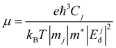 | (2) |
Here,
Cj,
mj, and |
Ejd| are the elastic constants, the effective mass of charge carriers, and the deformation potential in the
x and
y directions. The deformation potential is calculated as the change in band alignment under small tensile strain. The
m* is the geometrical average of effective mass of charge carriers along the
x and
y directions

.
T is the temperature and
e is the charge of the electron, while
kB is Boltzmann's constant.
For the accurate calculation of excitonic properties, the many body perturbation theory-based GW method is used.62 The GW calculations were performed by considering the unitcell of the JLs. Due to the high computational cost, single shot G0W0 calculations are performed using the Kohn Sham wavefunction obtained with the GGA functional as a starting point. The number of frequency grid points used for the frequency integration is 32. The GW band structure is calculated using maximally localized Wannier functions as implemented in the Wannier-90 code.63 On top of GW calculations, the BSE is solved to study the excitonic properties. A set of 256 virtual bands is used for the GW calculations. The k-grid was selected to be 12 × 12 × 1. We have considered 8 occupied bands and 16 unoccupied bands for the GW-BSE calculations.
3 Results and discussion
3.1 Structural properties and charge redistribution
We have designed six SnXY (X, Y = F, Cl, Br, I) JLs and investigated their phonon stability. The calculated phonon band structures of all these JLs are presented in the SI (Fig. S1–S6). We found that out of the six structures, only two are stable i.e., SnIBr and SnICl. Therefore, here we explore the structural, electronic, optical and catalytic properties of SnIX (X = Br/Cl) JLs in detail. The side and top views of the geometrically relaxed SnIX structures are illustrated in Fig. 1(a) and (b). In a unit cell with three atoms, Sn is sandwiched between halide layers with different electronegativities confirming the Janus nature of the designed structure. The predicted SnIBr and SnICl monolayers have a 1 T atomic arrangement in the trigonal geometry. Also, the structures possess C3v point group and P3m1 space group symmetry. The structural parameters of SnIX JLs and their parent layers SnI2 and SnX2 are presented in Table 1. The data for the SnI2 monolayers are in accordance with the experimentally reported values.64 It is found that the structural parameters of SnIBr are larger than those of the SnICl JLs. This is due to the larger atomic size of Br compared to the Cl atom. The large differences in the bond lengths between Sn–I and Sn–X bonds indicate the vertical asymmetry in the designed JLs. The asymmetry is larger for SnICl than for SnIBr JL. This broken symmetry may cause asymmetric charge distribution in the top and bottom layers of the JL. Furthermore, it is found that the bond angle created at the centre layer is larger for SnIBr (I–Sn–Br) compared to SnICl (I–Sn–Cl) JL. Due to this difference in the bond angle, the thickness of SnIBr varied from that of SnICl by 0.20 Å. This means that the thickness of these JLs can be tuned by the replacement of one of the halide sub-layers.
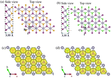 |
| | Fig. 1 The side and top views and the ELF (top view) of geometrically relaxed SnIBr ((a) and (c)) and SnICl ((b) and (d)) JLs. The ash, violet, orange and green circles represent Sn, I, Br and Cl atoms respectively. The yellow region represents the region with high electron localization. | |
Table 1 Calculated formation energy and structural parameters (lattice parameter, bond length, bond angle centred around the Sn atom, and thickness) of SnIBr and SnICl JLs and their parent structures SnI2, SnBr2, and SnCl2
| Structure |
Formation |
Lattice |
Bond length (Å) |
Bond angle (°) |
Thickness (Å) |
| Energy (eV) |
Parameter (Å) |
Sn–I |
Sn–X |
I–Sn–X |
| SnI2 |
−2.42 |
4.49 |
3.20 |
— |
90.86 |
3.75 |
| SnBr2 |
−2.93 |
4.33 |
— |
3.01 |
88.17 |
3.37 |
| SnCl2 |
−3.30 |
4.25 |
— |
2.88 |
84.87 |
3.02 |
| SnIBr |
−2.67 |
4.41 |
3.19 |
3.09 |
89.20 |
3.55 |
| SnICl |
−2.85 |
4.38 |
3.19 |
2.88 |
87.08 |
3.35 |
The electron localization function (ELF) of SnIX JLs with an isosurface value of 0.75 e Å−1 is shown in Fig. 1(c) and (d). It is the measure of the probability of finding an electron in the neighbourhood space of a reference electron located at a given point with a similar spin. From this perspective, the regions having high ELF have high electron localization. As shown in Fig. 1(c) and (d), the high ELF is found to be near the halide atoms. This indicates electron transfer from the Sn layer to the halide layers. The differential charge density plot was also calculated for both SnIBr and SnICl JL and is presented in Fig. S7. This shows that the charge is depleted from the Sn atom and accumulated near the halide atoms in both the JLs. The obtained result is in accordance with the result obtained from the ELF.A more detailed investigation on this issue is performed using Bader charge analysis. The calculated data are presented in Table 2. The nominal charge state of each element in the structure is given in brackets. Even though the nominal charge state of Sn is 2+, nearly half of the positive charge is depleted near Sn, and the other half is transferred to the atoms of both top and bottom layers. In SnIX JLs, the charge accumulated near the iodine atom is −0.45 e. Similarly, the charge accumulated near the X atom is −0.56 e and −0.65 e in the SnIX JL. From the obtained result, the Sn–I bond is more covalent in nature and Sn–X bond is more ionic in nature. The charge accumulation near the halide layers can also be compared with the electronegativity of each element on the Pauling scale. The electronegativity of Sn, I, Br and Cl are reported to be 1.96, 2.66, 2.96 and 3.16 respectively. The larger negative charge accumulation near the Cl atom compared to the Br atom may be due to the comparatively large electronegativity of Cl. The difference in charge accumulation between the top and bottom sublayers is calculated to be 0.20 e in the SnICl monolayer and 0.11 e in the SnIBr monolayer. The large electronegativity difference in the top and bottom sublayers of the SnICl JL leads to a relatively larger built-in electric field (see Section 3.6). This may improve the separation time of optically excited charge carriers, which will enhance the photocatalytic efficiency of the material.
Table 2 Results of Bader charge analysis for SnIBr and SnICl JLs and their parent structures SnI2, SnBr2, and SnCl2. Values are presented in units of elementary charge of electrons e
| Structure |
Sn (2+) |
I (1−) |
Br (1−) |
Cl (1−) |
| SnI2 |
0.91 |
−0.45 |
— |
— |
| SnBr2 |
1.13 |
— |
−0.56 |
— |
| SnCl2 |
1.30 |
— |
— |
−0.64 |
| SnIBr |
1.02 |
−0.45 |
−0.56 |
— |
| SnICl |
1.11 |
−0.45 |
— |
−0.65 |
3.2 Stability analysis
3.2.1 Formation energy.
The formation energy of the SnIX JLs and their parent structures is calculated using the formula| |  | (3) |
where Etotal is the total energy of a unit cell. Nj and μj are the number of atoms and chemical potential of atoms of species j in the unit cell respectively. The total energy calculated for the JLs and the corresponding parent structures are presented in the SI (Table S1). The chemical potentials of the halide atoms are obtained from the total energies of the halide dimers. The chemical potential of Sn is calculated from the total energies of cubic Sn. The corresponding data are given in Table S2. The halide dimers are used as references since the 2D JLs are usually formed by Chemical Vapour Deposition (CVD). The formation energies of the SnIX JLs and their parent structures are presented in Table 1. Negative formation energy indicates that the JLs and their parent structures are energetically stable. It is also noted that the formation energies of both the JLs are the average of formation energies of their respective parent structures.
3.2.2 Phonon stability.
The dynamic stability of the structures is studied using phonon vibrational spectra. The calculations performed without including Born effective charges are given in Fig. S1 and S2. Due to the intrinsic polar nature of the designed JLs, the Born effective charges are calculated and dipole corrections are incorporated into the phonon calculation. The obtained phonon spectra are given in the first column of Fig. 2. The lack of imaginary modes in the phonon spectra indicates the structural stability of designed structures. In these phonon spectra, there are 9 phonon modes present, including 3 acoustic modes and 6 optical phonon modes. The three acoustic phonon modes include longitudinal acoustic, transverse acoustic, and out-of-plane acoustic modes. The absence of a phonon gap between acoustic and optical modes indicates that there is strong phonon–phonon interaction in the designed JLs. From the phonon spectral analysis, it is found that the highest frequency of optical phonon mode is 4.3 THz for SnIBr and 5.2 THz for SnICl monolayers. The lower phonon frequency of the SnIBr monolayer is due to the larger atomic size of the Br atom compared to the Cl atom. The calculated phonon density of states of SnIX JLs is presented in Fig. S8. From Fig. S8(a) and (b), it is found that all the elements contribute to phonon density of states. Also, elements having lower atomic weight contribute more to the high-frequency range and elements having larger atomic weight contribute more to the low-frequency range.
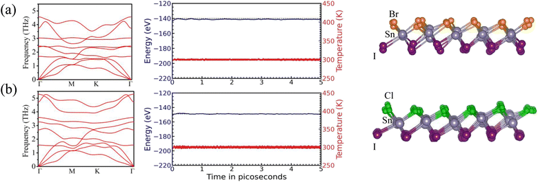 |
| | Fig. 2 The phonon band structure (first column) and energy (blue line) and temperature (red line) fluctuation during AIMD simulation (second column) and snapshot of the geometrical structure at the end of AIMD simulation (third column) of SnIBr (a) and SnICl (b) JLs. The AIMD simulation was performed at 300 K temperature for a period of 3 ps (time step: 0.51 fs). | |
3.2.3 Thermal stability.
To study the stability of the structure under ambient conditions AIMD calculations are performed for 3 ps with a time step of 0.51 fs. The temperature and total energy fluctuations of SnIBr and SnICl monolayers and the geometrical structure after the AIMD simulation are shown in the second and third columns of Fig. 2. For the SnIBr monolayer, the total energy fluctuation is ±0.2 eV and temperature fluctuation is ±10 K (middle column of Fig. 2(a)). The total energy variation of SnICl is ±0.3 eV and temperature fluctuation is ±15 K (middle column of Fig. 2(b)). Compared to the SnIBr monolayer, the energy and temperature fluctuation are found to be somewhat larger in the SnICl monolayer. The geometrical structure after the AIMD calculation shows negligible atomic distortion without breaking the bonds. The unbroken structure and the low energy and temperature fluctuation indicate the thermal stability of the predicted monolayers at room temperature. We also performed AIMD simulation at 500 K for a period of 5 ps. At 500 K, also, the temperature and energy fluctuation are found to be low (Fig. S9). Our result shows that the SnIX JLs are stable at 500 K.
3.2.4 Mechanical stability.
The mechanical stability of the SnIBr and SnICl JLs is verified from the independent elastic constants C11 and C12. The elastic constants are calculated with the help of a second-order derivative of total energy versus the strain curve within the range of Hooke's law. The elastic constants indeed met the Born stability criteria for the 2D trigonal structures i.e., C11 > 0 and C11 > C12.
Furthermore, Young's modulus (Y), Poisson's ratio (ν) and shear modulus (G) are calculated and presented in Table 3. From Table 3, SnICl shows a slightly increased Young's modulus compared to SnIBr with a difference of 0.5 N m−1. But, compared to other traditional 2D materials such as graphene (340 N m−1),65 and MoSSe (113 N m−1),66 SnIBr and SnICl exhibit lower values. This indicates lower elastic stiffness or high flexibility of the designed structure. The polar representation of the in-plane (x–y) variation of Young's modulus and Poisson's ratio is presented in Fig. S10. This suggests that the mechanical properties show an in-plane isotropic nature in the designed SnIX JLs.
Table 3 Calculated elastic constants (C11, C12), Young's modulus (Y), shear modulus (G), and Poisson's ratio (ν) of SnIX (X = Br, Cl) JLs
| Structure |
C
11 (N m−1) |
C
12 (N m−1) |
Y (N m−1) |
G (N m−1) |
ν
|
| SnIBr |
17.55 |
4.67 |
16.31 |
6.44 |
0.26 |
| SnICl |
18.24 |
5.11 |
16.81 |
6.56 |
0.28 |
3.3 Phase diagram
To acquire insight into chemical conditions for the synthesis of JLs, a static phase diagram needs to be obtained. The chemical potential of an element can be defined asμ0j is the chemical potential of the reference state and Δμj is the change in chemical potential in the compound with respect to its reference state. The general thermodynamic constraint for the synthesis of the JL is Δμj ≤ 0. This indicates that the maximum range of the chemical potential of an element is the chemical potential of its reference state. This is considered to be the rich condition of the element. In the case of Sn, the cubic (Fd![[3 with combining macron]](https://www.rsc.org/images/entities/char_0033_0304.gif) m) structure is considered the reference state, and for the halides the reference is the energy per atom in the corresponding dimer, since the JLs are usually formed by Chemical Vapour Deposiition (CVD). Furthermore, to calculate the chemical potential of elements under poor conditions, Δμj is calculated from the stability conditions of the parent material (SnI2, SnBr2 and SnCl2). The corresponding formation energy required to form the JL can be written as
m) structure is considered the reference state, and for the halides the reference is the energy per atom in the corresponding dimer, since the JLs are usually formed by Chemical Vapour Deposiition (CVD). Furthermore, to calculate the chemical potential of elements under poor conditions, Δμj is calculated from the stability conditions of the parent material (SnI2, SnBr2 and SnCl2). The corresponding formation energy required to form the JL can be written as| | | Hf[SnIX] = ΔμSn+ΔμI + ΔμX | (5) |
During the synthesis process of a JL, there is also a chance of the formation of the corresponding parent structures, which are considered the competing phases. The constraints due to the formation of parent structures are:67,68
| | | Hf[SnI2] ≥ ΔμSn + 2ΔμI | (6) |
| | | Hf[SnX2] ≥ ΔμSn + 2ΔμX | (7) |
We found that it is not possible to find a region which satisfies all these constraints. Hence we discuss the formation of the JL initiated from one of the parent structures. The synthesis of the JL from the parent structure is discussed in the framework of possible CVD techniques. Consider the synthesis method starting from the SnI2 monolayer. Here, one of the I layers in the parent structure (SnI2) can be replaced by atoms introduced by the purging gas containing halide dimers. The conditions for the replacement are determined by the chemical potential of the atoms in the dimers. In this aspect we can remove one of the constraint equations and the chemical potential variation can be represented in a static 2D phase diagram. The design method for the 2D static phase diagram for the synthesis of the SnIX JL from the SnI2 parent structure is presented here. The thermodynamic requirement for the formation of SnIX from SnI2 can be written as below:
| | | Hf[SnIX] = E(SnIX) − E(SnI2) − μX + μI | (8) |
Here,
Hf[SnIX] is the corresponding formation energy of the SnIX structure. The
E(SnIX),
E(SnI
2) are the total energies of SnIX and SnI
2 monolayers. By fixing the chemical potential of I at a rich or poor limit, the chemical potential of X can be varied from the rich limit to the poor limit using the thermodynamic conditions for the enthalpy of formation of parent materials. The chemical potential of Sn is fixed to rich conditions, since we are not tuning the middle atomic layer in the SnI
2 structure,
i.e. Δ
μSn = 0. With this condition, the value of Δ
μI under poor conditions can be calculated.
| | | Hf[SnI2] = ΔμSn + 2ΔμI | (9) |
In the same way, the synthesis of SnIX can be initiated from the SnX2 monolayer. For that, eqn (8) can be modified as
| | | Hf[SnIX] = E(SnIX) − E(SnX2) − μI + μX | (10) |
where the
E(SnX
2) is the total energy of SnX
2. In this particular case, we fix the chemical potential of X at a rich or poor limit; the chemical potential of I can be tuned from the rich limit to the poor limit by considering the condition of enthalpy of formation of the SnX
2 monolayer.
| | | Hf[SnX2] = ΔμSn + 2ΔμX | (11) |
Again, the chemical potential of Sn can be fixed to rich conditions, since we are not varying the middle atomic layer. Then, ΔμSn = 0 and, for X poor conditions, ΔμX can be obtained from eqn (11).
The phase diagram calculated for the design of the SnIX monolayers from SnX2 and SnI2 is presented in Fig. 3(a) and (b). The total energy of SnIX structures and their parent structures used for the calculation of the phase diagram is presented in Table S1. The chemical potential data of the reference states used in the calculations are presented in Table S2. In Fig. 3, the negative formation energy region represents the possibility of the formation of the SnIX JL with a variation of chemical potential. We found that the formation energy extends to the positive region only when the synthesis is initiated from the SnI2 monolayer. Among different conditions, we found that the halide poor condition is more favourable for the formation of both the JLs.
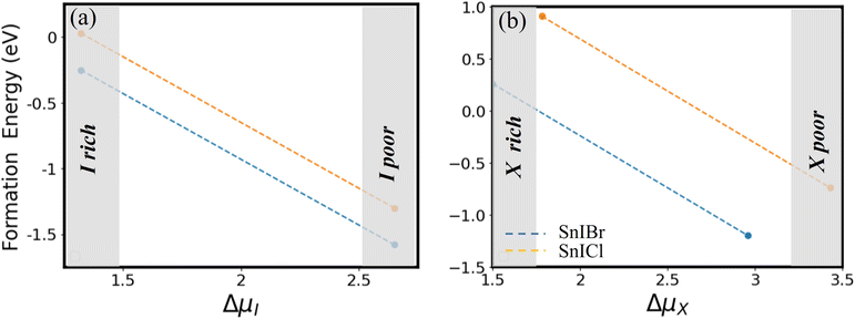 |
| | Fig. 3 The two-dimensional phase diagram for the design of SnIBr and SnICl JLs from SnX2 (a) and SnI2 (b) monolayers using halide dimers. | |
3.4 Effective mass and mobility of electrons and holes
The overall efficiency of a photocatalyst is determined by the fundamental efficiency of the material in visible light absorption, generation and annihilation of excitons, carrier migration and the water redox reactions. Therefore, in the following subsections, we investigate these four steps in detail.
The electronic properties of the SnIX JLs are investigated with the help of electronic band structure and density of states calculations (Fig. 4). The electronic band structure calculated along the high symmetry points of the Brillouin zone of SnIBr and SnICl JLs using GGA and HSE functionals is presented in Fig. 4(a) and (c). The GGA functional predicts an indirect band gap of 2.24 eV and 2.47 eV for SnIBr and SnICl monolayers respectively. The use of the HSE functional leads to an increase in the band gap of SnIBr to 2.99 eV and SnICl to 3.23 eV, without any significant change in the dispersion of bands. The conduction band minima (CBM) of both the JLs are at the centre of the Brillouin zone, i.e. at the Γ point. The valence band maxima (VBM) of SnIBr JL are in between the K and Γ points and for the SnICl JL, VBM are at the K point. The synergistic effect of the indirect and wide nature of the band gap may increase the charge separation time of the photogenerated carriers, which will be helpful for reducing the charge recombination rate in the photocatalysts.
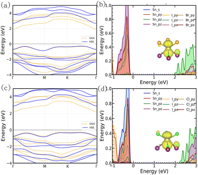 |
| | Fig. 4 The electronic band structure and orbital resolved density of states of SnIBr (a) and (b) and SnICl (c) and (d) JLs. The band structures calculated using GGA and HSE functionals are presented by dashed and solid lines respectively. In the band structure, red and blue dots represent VBM and CBM respectively. The partial charge density at CBM is shown in the inset of the density of states plot. The yellow surface marks the pz orbital of Sn. | |
Following the optical excitation of charge carriers, the next step is the migration of separated electrons and holes to the catalytic active centres at the surface. Thus, we have estimated the carrier mobility along the x and y directions of SnIX JLs. For this, the effective mass of carriers along the x and y directions is probed from band dispersion and the deformation potential is calculated along the x and y directions. The data obtained are summarized in Table 4. m0 indicates the bare mass of the electron. The data show the isotropic nature of electron effective mass and the anisotropic nature of the hole effective mass along the x and y directions. This is attributed to the symmetric dispersion of the conduction band around CBM and the asymmetric dispersion of the valence band around VBM. Also, the effective masses of electrons are found to be low compared to holes. From the obtained carrier effective mass and deformation potential, the mobility of the charge carriers is calculated. From Table 4, the anisotropic nature of carrier mobility along x and y directions is observed, which is due to the anisotropic nature of deformation potential as well as hole-effective mass. The carrier mobility is relatively high in the x direction. The electron mobility along the x direction is as high as 2.88 × 10³ and 1.55 × 103 cm2 V−1 s−1 for SnIBr and SnICl respectively. Similarly, hole mobility is noted to be 0.15 × 10³ and 0.18 × 103 cm2 V−1 s−1 for SnIBr and SnICl monolayers respectively. Table S3 shows that the SnIBr and SnICl JLs possess electron mobility higher than that of the other reported 2D materials. It is also important to note that electron mobility is significantly higher than that of holes which is beneficial for quick carrier separation, which is desirable for efficient water reduction and oxidation reactions.
Table 4 Basic electronic properties such as the band gap, effective mass (m*) of charge carriers, deformation potential (Ejd) and mobility (μ) of charge carriers (m0 is the mass of a bare electron)
| Structure |
Band gap (eV) |
Carrier |
m* (m0) |
E
j
d (eV) |
μ (103 cm2 V−1 s−1) |
| GGA |
HSE |
GW |
x
|
y
|
X
|
y
|
x
|
y
|
| SnIBr |
2.24 |
2.99 |
3.63 |
Electrons |
0.08 |
0.08 |
4.41 |
6.17 |
2.88 |
0.39 |
| Holes |
0.24 |
0.46 |
6.61 |
5.29 |
0.15 |
0.01 |
| SnICl |
2.47 |
3.23 |
3.92 |
Electrons |
0.09 |
0.09 |
5.59 |
6.45 |
1.55 |
0.32 |
| Holes |
0.68 |
0.67 |
2.15 |
2.58 |
0.18 |
0.03 |
The orbital resolved density of states of the SnIBr and SnICl monolayers are presented in Fig. 4(b) and (d). In both structures, it is observed that the VBM and CBM are constructed out of the p orbital of the atoms present. It is also important to mention that the conduction band is dominated by the pz orbital of the Sn atom. The partial charge density calculated at the CBM verifies this result. The presence of z-directional pz orbitals at the CBM position suggests that the optical excitation is due to the orbital having out-of-plane orientation with respect to the 2D layer. Since the optical excitation and the built-in electric field (see Section 3.6) are in the same direction in these JLs, the possibility of charge recombination can be reduced considerably.
The synergetic effect of the built-in electric field, the large disparity in electron–hole mobility, and the presence of out-of-plane-oriented conduction band orbitals enhance the separation time of electrons and holes, which will make a positive impact on the overall efficiency of the material.
3.5 Excitonic properties
In order to calculate the excitonic properties, we employed many-body perturbation theory using the GW method and the Bethe Salpeter equation. At first, single-shot GW calculations were performed with the converged DFT results as input. Then, we solved the Bethe Salpeter equation on top of the GW calculation. The calculated band structure and the linear frequency-dependent dielectric spectra determined with (GW-BSE) and without (GW-RPA) the excitonic effect are presented in Fig. 5. The GW indirect band gaps of SnIBr and SnICl JLs were calculated to be 3.63 eV and 3.92 eV respectively (first column of Fig. 5, see also Table 4). Also, the GW-direct band gaps of the SnIX JLs are found to be 4.13 and 4.30 eV respectively. It is noted that there is not much change in the dispersion of the band structure compared to the GGA and HSE level approximations.
In the second column of Fig. 5, the GW-RPA and GW-BSE dielectric spectra of both SnIBr and SnICl are presented. The GW-RPA spectra show significant peaks in the high-frequency range (4–8 eV). The broad peaks indicate the transitions due to the bands which are not perfectly parallel. After electron–hole interactions are included (GW-BSE data), a prominent change in the dielectric spectra was observed. The GW-BSE dielectric spectra show a wide range of light absorption with the maximum in the UV region. The red shift of the spectra with sharp peaks in the low frequency (3–5 eV) regime is a noticeable change compared to the GW-RPA results.
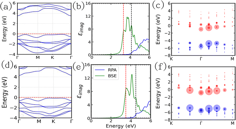 |
| | Fig. 5 The GW band structure (first column), the imaginary part of the dielectric constant calculated with (GW-BSE) and without excitonic (GW-RPA) interaction (second column) and the illustration of fatband analysis (third column) of SnIBr (a–c) and SnICl (d–f) JLs. The red dashed line represents the Fermi level. In dielectric constant spectra, the red and black dashed lines represent the first excitonic peak (optical band gap) and the GW direct band gap, respectively. In fat band analysis, the red and blue circles represent electrons and holes respectively. The radius of the circle represents the coupling coefficient. | |
The excitonic binding energy is one of the important parameters, which dictates the lifetime of the excitons. Thus, the excitonic binding energy of the material was calculated from the difference between the first bound excitonic peak (optical gap) and the GW-direct band gap. It was found that excitonic binding energy is 0.60 eV and 0.97 eV for SnIBr and SnICl JLs respectively. Since it is higher than the energy of a thermally excited phonon (25 meV), the excitonic effects cannot be neglected. The exciton binding energy of SnIBr and SnICl was compared to that of the conventional 2D structures and was found to be lower than that of graphene which is reported to be 1.77 eV.69 But it is in the same range as that of other prototype JLs MoSSe (0.85 eV)66 and WSSe (0.83 eV).70 The lower excitonic binding energy of the SnIBr JL may be due to the large dielectric constant compared to the SnICl JL. The larger the dielectric constant, the larger the screening effect between electron–hole pairs.
Another method to calculate the excitonic properties is the classical Mott–Wannier (MW) model. In this model, we consider excitons as the bound state of electrons and holes and calculated the excitonic binding energy using:
| |  | (12) |
where
μex is the effective excitonic mass. This is calculated from the reduced mass of electrons and holes at CBM and VBM respectively,
i.e.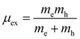
. The
εr is the calculated dielectric constant of the material. The excitonic binding energy is calculated to be 0.57 eV in the SnIBr monolayer and 0.77 eV in the SnICl monolayer. This is smaller than that obtained from the GW-BSE spectra. Differences between the GW and MW results were also reported for other unsymmetrical 2D structures.
71,72 Within the Mott–Wannier model, the excitonic radius is calculated using
| |  | (13) |
where
m0 and
aB are the mass of the bare electron and Bohr radius respectively. We calculated the excitonic radius in SnIBr and SnICl JLs and it was found to be 2.00 nm and 1.54 nm respectively. These data show that there is an order difference between the electron–hole separation distance and the atomic spacing in the designed structures. The large electron–hole separation hints at free excitons which can diffuse across the material. This contributes to carrier separation after photoexcitation. Finally, to study the electron–hole coupling in the SnIX JLs, the calculations are performed on the first excitonic peak of GW-BSE spectra and the generated fat band results are presented in the last column of
Fig. 5. The excitonic interactions are observed in the region
K–
Γ–
M. The electrons and holes are represented by red and black circles in the JLs. The radius of the circles indicates the coupling coefficient of excitons. From the illustration, it is clear that the exciton distribution in
Γ–
K and
Γ–
M is different in both the JLs. This may be due to the different asymmetrical dispersion of the conduction band and valence band around the
Γ point.
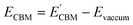
3.6 Electrostatic potential energy and band alignment
To investigate the water redox ability of the designed JLs, the calculated planar averaged electrostatic potential energy at the GGA level and the BA at GGA, HSE and GW level approximations are presented in Fig. 6. In the electrostatic potential energy diagram, there is a small difference in the vacuum level between the top and bottom sub-layers of the JL i.e., I and X layers. This is marked as a dashed line in Fig. 6(a) and (c). The difference in the vacuum level (Δϕ) is observed to be 0.21 eV in SnIBr and 0.36 eV in the SnICl JL. This is due to the asymmetric charge distribution in the top and bottom layers, which we already observed from the Bader charge analysis. The aforementioned charge difference causes a built-in dipole along the out-of-plane direction in both JLs. This will cause a built-in electric field in the JLs. The direction of the built-in electric field is found to be from the lower to the higher electronegative surface in the SnIX JLs (I sublayer to the X sublayer). The built-in electric field polarises the electrons and holes in opposite directions, i.e. the electrons are transferred in the opposite direction of the created electric field. We have also calculated the built-in electric field quantitatively. To calculate the built-in electric field, we have used the equation| |  | (14) |
Here, Δv is the change in electrostatic potential from the top layer to the bottom layer of the SnIX monolayer and Δr is the distance between the top layer and the bottom layer. In SnIBr, the Δv and Δr values are calculated to be 5.71 eV and 3.55 Å respectively. In SnICl Δv and Δr are 4.36 eV and 3.33 Å. We obtained the built-in electric field in SnIBr and SnICl JL 1.60 eV Å−1 and 1.30 eV Å−1.
Furthermore, the BA of the SnIX JLs is calculated based on the GGA, HSE and GW methods using the equation
| |  | (15) |
| |  | (16) |
Here,

and

are calculated VBM and CBM, without shifting the Fermi level to zero.
Evacuum is the vacuum level corresponding to the more electronegative sublayer in the JLs.
i.e., the Br layer in SnIBr and the Cl layer in SnICl JL. We have calculated the VBM and CBM band edge levels using DFT with GGA and HSE exchange-correlation functionals and with the single-shot GW method. We found that the vacuum level is insensitive to the exchange-correlation functional in the case of SnIX JLs. Based on the assumption that the vacuum level is not changed in the many-body perturbation theory, we have calculated the BA of SnIX structures. The BA diagram is depicted in
Fig. 6 and the related data are presented in Table S4. To study the water redox ability of the JLs, BA needs to be compared with water reduction and oxidation potentials. The water redox potentials are pH-dependent based on the equation shown
73 (in eV):
| |  | (17) |
| |  | (18) |
 |
| | Fig. 6 The planar averaged electrostatic potential energy and band alignment diagram of SnIBr ((a) and (b)) and SnICl ((c) and (d)) JLs. In the electrostatic potential energy diagram, the vacuum level with respect to different electronegative surfaces is represented by dashed lines. In the band alignment diagram, the black and red lines represent water reduction and oxidation potentials with respect to the vacuum level at pH = 0. | |
We have compared BA with redox potentials under three different pH conditions pH = 0 (acidic), pH = 7 (neutral), and pH = 14 (alkaline). The obtained results are presented in Fig. 6(b) and (d) and in Fig. S11. For the overall water splitting, water reduction and oxidation potentials must straddle the CBM and VBM respectively. This condition is fulfilled for the band alignment obtained using DFT with GGA and HSE functionals and for that determined by the single-shot GW method in the case of pH = 0 (Fig. 6). Fig. S11 shows that in the case of GW data the water reduction and oxidation potentials are between CBM and VBM under all three pH conditions considered. The GGA and HSE results exhibit a different behavior. For the GGA, the above-mentioned conditions for water splitting are only fulfilled for pH = 0 and for HSE functional, they are only fulfilled for pH = 0 and 7.
In the case of SnIBr and SnICl JLs, the CBM of GW level BA is 1.03 eV higher than that of water reduction potential at pH equal to zero. Under light-on conditions, the charge carriers are providing this extra 1.03 eV energy, for the reaction to occur. This is the highest available energy that can be provided by the charge carriers. Hence acidic conditions (pH = 0) are found to be the most favourable conditions for the reduction reaction to be carried out for both the JLs. Under all pH conditions, the oxidation potential is situated above the VBM. Among the different pH conditions, the most favourable reaction conditions for the oxidation reaction are alkaline conditions (pH = 14). This is due to the additional energy, provided by the holes. This energy is noted to be 2.6 eV for SnIBr and 2.89 eV for SnICl monolayers respectively. This additional energy helps the oxidation reaction to proceed spontaneously.
3.7 Overall water splitting
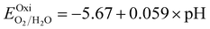
Photocatalytic hydrogen production is considered an overall water-splitting reaction in which water reduction and oxidation take place in the same material. The water reduction reaction is a two-step process that includes adsorption and desorption of hydrogen on SnIBr and SnICl JLs. Generally, these reactions can be expressed as74| | | H* + H+ + e− → H2 + * | (20) |
Here, * is the substrate i.e. SnIX JLs. In the first step, a proton gets adsorbed on an active site of the substrate where an electron is transferred and an H-substrate complex is formed. This hydrogen adsorption reaction step is called the Volmer reaction. The second step is the H2 releasing step or desorption reaction step. The as-provided desorption reaction mechanism is called the Heyrovsky mechanism. The illustration of the reaction steps in SnIBr and SnICl JLs are presented in Fig. 7(a) and (b). In contrast to the simple two-step water reduction reaction, the water oxidation reaction is a complex multistep reaction mechanism. All four steps in the water oxidation reaction are carried out with the consumption of holes. The first three steps include the formation of complexes such as OH*, O*, and OOH*. These are the molecule adsorption steps in the water oxidation reaction. The final step is the release of the O2 molecule from the substrate. The mentioned four steps can be represented as75| | | * + H2O + h+ → OH* + H+ | (21) |
| | | O* + H2O + h+ → OOH* + H+ | (23) |
| | | OOH* + h+ → * + O2 + H+ | (24) |
The illustration of this four-step water oxidation reaction on the JL is presented in Fig. 7(c) and (d). In each step, there is a release of H+ ions, which will take part in the reduction reaction. From Fig. 7, we found that the reaction steps for forming substrate-molecule complexes are critical. Hence, not only the band alignment positions but also the active catalytic sites are important for the performance of a photocatalyst. The latter is investigated in the following sections.
 |
| | Fig. 7 The illustration of water reduction and the oxidation reaction in SnIBr (a) and (c) and SnICl (c) and (d) JLs. We have presented geometrically relaxed structures of JLs and intermediate complexes. The red and blue atoms in the reaction steps indicate hydrogen and oxygen atoms respectively. | |
3.7.1 Active layers for water redox reactions.
The active surface favorable for the reduction and oxidation reactions is selected based on the spatial separation of charge carriers, the built-in electric field and the existing polarisation direction. From the planar averaged electrostatic potential calculation, we found that the electric field direction is from the lower electronegative I layer to the higher electronegative X layer. As a result, electrons will flow from the X layer to the I layer. Due to this charge separation, electrons will be more available near the I layer and holes will be more near the X layer. Since the water reduction reaction required electrons from the substrate, the I layer is more suitable. Similarly, the X layer is more suitable for the water oxidation reaction due to the large availability of holes.
3.7.2 Gibbs free energy change in water redox reactions.
The reaction energy during hydrogen adsorption and desorption in the water reduction reaction, see eqn (19) and (20), is given by| |  | (25) |
| |  | (26) |
Here, EH* and E* are the total energy of the H-substrate complex and substrate respectively. EH2 is the total energy of an isolated hydrogen dimer molecule. Adding eqn (25) and (26) leads to (ΔE1 + ΔE2 = 0) zero. This indicates that the sum of the reactions (19) and (20) has zero reaction energy under standard temperature and pressure conditions. Therefore the GFE before and after the reaction is the same under light-off conditions, see e.g.Fig. 8(a) and (b). The relaxed geometry of the H-substrate complex is presented in Fig. 7. The hydrogen is adsorbed on the top of the I atom with a bond distance of 1.65 Å on both SnIBr and SnICl JLs. From SnIBr JL, a 0.92 e charge is transferred to the hydrogen atom, whereas 0.93 e charge is transferred from the SnICl JL to the hydrogen atom during the hydrogen adsorption reaction step. By analysing the geometry after the structural relaxation, we have noticed a small local distortion on the H-adsorbed I atom. However, the overall structure is found to be quite stable. Similarly, the adsorption energy of OH, O, and OOH on the substrate during the oxidation reaction and energy change in the O2 desorption step, see eqn (21)–(24), are
| |  | (27) |
| |  | (28) |
| |  | (29) |
| |  | (30) |
where EOH*, EO*, EOOH* and E* are the total energies of OH-substrate, O-substrate, and OOH-substrate complexes and the substrate respectively. The EH2O and EO2 are the energies of isolated H2O and O2 molecules respectively.
 |
| | Fig. 8 The illustration of the GFE water reduction and oxidation profiles in SnIBr (a) and (c) and SnICl (b) and (d) JLs calculated at pH equal to zero. | |
The calculated total energies of the substrate, substrate-molecule complexes and the molecules are presented in Table S5. All the adsorption energies are determined for the geometrically relaxed structures using a 5 × 5 × 1 supercell. The geometrically relaxed structures of intermediate complexes in the reaction steps are presented in Fig. 7(c) and (d). Even after the relaxation of the substrate-molecule complexes, the distortion of the atoms is found to be minimal. We have tried molecular adsorption on the different sites of the JLs. The OH molecule is stable near the substrate when the molecule aligns parallel to the JL on the top of the X atom. This OH-molecule forms a bond with the substrate with a length of 2.29 Å in both the JLs. In the case of the O-substrate complex, the more energetically favorable position for O is on top of the X layer with a distance of 1.57 Å and 1.56 Å for SnIBr and SnICl respectively. In the case of the OOH molecule, we found that the molecule is stable on the top of the JL with an arched arrangement of atoms.
Finally, the thermodynamic favorability of the water reduction and oxidation reactions is studied by investigating the change in Gibbs free energy ΔG in each reaction step.76,77
| | | ΔG(T) = ΔE + ΔEZPE − TΔS − ΔGU | (31) |
Δ
E is the energy of the reactions
(19)–(24) given in
eqn (25)–(30). Δ
EZPE and Δ
S are the changes in zero point energy and entropy during these reactions which can be calculated similar to the reaction energies (
eqn (25)–(30)). Zero-point energy calculations for the water reduction reaction in the SnIBr monolayer were performed and found to be negligible. Considering the high computational cost in calculating the zero point energy of the substrate-molecule complex, we neglect this contribution also in other cases. Furthermore, we also found that the entropy of the solid substrate is less compared to the gaseous molecule. Hence, we only consider the entropy of gaseous states at standard temperature and pressure, which is obtained from the NIST database (NIST Computational Chemistry Comparison and Benchmark Database (https://cccbdb.nist.gov/)). The data for
TΔ
S are given in Table S5. The final term, Δ
GU, considers the contribution due to the formation of electrons and holes under light-on conditions. It is related to the so-called overpotential,
i.e. an extra potential. This is calculated as −
nU, where
n is the total number of electrons that take part in the reaction and
U is the overpotential. The as-mentioned overpotentials for the water reduction and oxidation reactions are calculated as follows:
| |  | (32) |
| |  | (33) |
Here,
ECBM and
EVBM are the quantities given in
eqn (15) and
(16). Also,

and

are water reduction and oxidation potentials which depend on different pH conditions, see
eqn (16) and
(17), and Δ
ϕ is the difference in the vacuum level of top and bottom sublayers in the JLs which is obtained from
Fig. 6(a) and (c).
The calculated overpotential for the water reduction reaction and oxidation reaction is presented in Table 5. In the case of the water reduction reaction, the overpotential calculated for GGA BA is very small. The negative overpotential indicates an additional amount of energy needed to carry out the reaction. Based on GGA and HSE BAs in the SnIBr monolayer, the reduction reaction is difficult at a pH equal to 14. The GGA results for SnICl show that the reduction reaction is also hardly possible under alkaline conditions. The highest reduction overpotential is provided under neutral conditions in the GW level BA in both the JLs i.e., 1.24 eV for SnIBr and 1.39 eV for SnICl monolayers. In the case of the oxidation reaction, the alkaline conditions provide the highest overpotential in both the JLs. The highest overpotential for SnIBr is 3.42 eV and for SnICl it is 3.71 eV, which are calculated using alkaline conditions and GW BA.
Table 5 The calculated overpotentials with respect to the standard hydrogen electrode potential for water oxidation and reduction reactions under different pH conditions
| pH |
Overpotential-HER (eV) |
Overpotential-OER (eV) |
| SnIBr |
SnICl |
SnIBr |
SnICl |
| GGA |
HSE |
GW |
GGA |
HSE |
GW |
GGA |
HSE |
GW |
GGA |
HSE |
GW |
| 0 |
0.57 |
0.80 |
1.24 |
0.71 |
0.97 |
1.39 |
1.88 |
2.40 |
2.60 |
2.11 |
2.62 |
2.89 |
| 7 |
0.16 |
0.39 |
0.83 |
0.30 |
0.56 |
0.98 |
2.29 |
2.81 |
3.01 |
2.52 |
3.03 |
3.30 |
| 14 |
−0.25 |
−0.02 |
0.42 |
−0.11 |
0.15 |
0.57 |
2.70 |
3.22 |
3.42 |
2.93 |
3.44 |
3.71 |
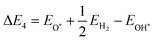
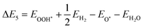
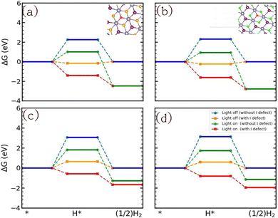
The GFE profile of the water reduction mechanism is presented in Fig. 8(a) and (b) for the case of pH = 0 (acidic conditions). Under light-off conditions, the GFE required for the reaction is as high as 2.25 eV and 2.32 eV for SnIBr and SnICl JLs. Under light-on conditions, the negative charge carriers will provide energy, which is given by the overpotential. Compared to the light-off case, under light-on conditions for SnIBr the GFE change in the Volmer reaction step (eqn (19)) is reduced by 0.57 eV (GGA), 0.80 eV (HSE) and 1.24 eV (GW), cf.Table 5. The GW-based GFE change in the first reaction step is 1.01 eV. Using a similar approach for SnICl, the light-on GW-based GFE change in the first reaction step is 0.93 eV. While the first reaction step (adsorption, eqn (19)) is endergonic, since the GFE change is positive, the second (desorption, eqn (20)) is exergonic, i.e. the value of GFE decreases. We have also investigated the GFE change under other pH conditions such as pH equal to seven and fourteen and presented it in the SI (Fig. S12). It is found that the GFE change in the first reaction step increases with increasing pH values so pH = 0 is most favorable.
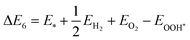
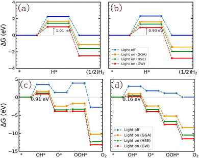
Furthermore, we investigated the GFE profile of the water oxidation mechanism. The reaction step with the highest positive GFE change (endergonic step) decides the overall water oxidation performance (rate-determining step, RDS). Under light-off conditions, the rate-determining step (OH* formation step) is as high as 3.51 eV for SnIBr and 3.05 eV for the SnICl monolayer. Under light-on conditions, there is a decrease in GFE of the reaction due to the additional energy provided by the charge carriers. The GFE profile under light-on conditions was studied based on the GGA, HSE and GW level band alignments under different pH conditions. The results corresponding to pH equal to 0 are presented in Fig. 8(c) and (d). Also, the pH 7 and pH 14 results are presented in Fig. S13 and S14 respectively. The more accurate GW level results show a stronger GFE decrease (for the reaction steps) than data obtained by HSE and GGA methods. For both JLs, under light-on conditions the OH* formation step is still endergonic, but with much smaller GFE change (0.91 eV for SnIBr and 0.16 eV for SnICl) than that in the light-off case. All other steps are exergonic (GW level data). Fig. S13 and S14 in the SM demonstrate that the GFE of the steps can be further reduced at pH equal to 7 and 14. For SnIBr, at pH equal to 7 and 14 the GFE of the OH* formation step is 0.50 and 0.09 eV respectively. In the case of SnICl GFE, data of −0.25 and −0.66 eV were obtained for pH = 7 and 14, respectively. This means that in some cases all the steps of water oxidation are exergonic and the OER is spontaneous.
3.8 Defect engineering
The positive impact of defects in improving the efficiency of the photocatalyst was already reported.48,78 Since we have found that the iodine surface is more suitable to perform the water reduction reaction, we study the effect of an iodine monovacancy in a 5 × 5 × 1 supercell. When hydrogen was placed in the space where the iodine vacancy is situated, it moved near the Sn atom and adsorbed. Fig. S15(a) and (b) shows the relaxed H-adsorbed SnIBr and SnICl JLs with the iodine vacancy. Also, we found that the whole geometrical structure did not change significantly after relaxation. Hence, we performed a detailed analysis of the H adsorbed on the Sn atom. To study the charge transferred to the hydrogen atom from the substrate, Bader charge analysis was performed. It is observed that a −0.44 e charge is transferred to H from SnIBr. The charge transfer in the SnICl Janus layer has the same value. This shows that the change in the X sub-layer in the SnIX JL does not affect the hydrogen adsorption on the I surface. We also noticed that there is a decrease in the charge transfer compared to that of the H* complex formed in the bare structure. The GFE profile of the water reduction reaction (pH = 0 and pH = 14) after introducing the I vacancy in SnIBr and SnICl JL is presented in Fig. 9. A snapshot of the top view of the geometrically relaxed hydrogen-substrate complex with the vacancy is provided in the inset of Fig. 9(a) and (b). Under acidic conditions, the GFE change shows that the H* complex formation is exergonic. Even under the light-off conditions, the GFE change in the Volmer reaction is −0.16 eV for SnIBr and −0.23 eV for the SnICl JLs. Under the light-on conditions, the GFE change is more negative which is measured to be −1.40 eV for SnIBr and −1.62 eV for SnICl JLs. Here, we found that the adsorption reaction will be spontaneous due to the negative GFE change under both light-off and light-on conditions. Under light-on conditions, the desorption is also exergonic. Our result shows that the iodine vacancy is helping the HER to be spontaneous under acidic conditions. We have also investigated the GFE change under alkaline conditions, which is presented in Fig. 9(c) and (d). Under alkaline conditions, the results associated with light-off conditions show that the GFE change in the Volmer reaction reduced significantly compared to that of the bare structure. Still, it is not spontaneous due to the GFE change associated with the light-off conditions which is reported to be 0.66 eV for SnIBr and 0.59 eV for SnICl. In the light-on case, the GFE change reduced to −0.58 eV and −0.80 eV in SnIBr and SnICl JLs respectively, which means an exergonic adsorption reaction. Also, the desorption is exergonic.
 |
| | Fig. 9 The GFE profile in the presence of an I monovacancy in SnIBr at pH = 0 (a) and pH = 14 (c) and in SnICl at pH = 0 (b) and 14 (d). A snapshot of the H-substrate complex is presented in the inset. | |
3.9 Strain engineering
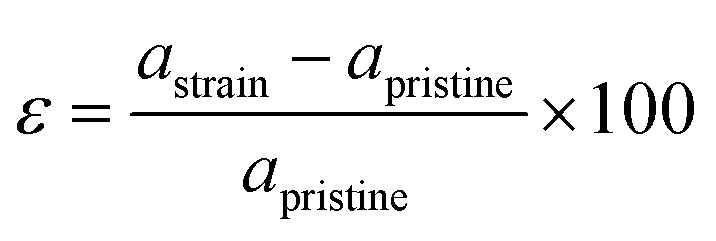
2D materials are mainly grown on a certain substrate. Due to the lattice mismatch with the substrate, the deposited 2D materials are usually under strain. It is reported that the effect of strain leads to significant changes in the electronic, optical and catalytic properties of the material. In particular, 2D materials show drastic change due to the ultra-low thickness and mechanically flexible characteristics. In this section, we systematically investigate the effect of biaxial and uniaxial lateral strain engineering on the electronic and photocatalytic properties of the newly designed SnIBr and SnICl JLs. The applied strain percentage in JLs is calculated as follows:| |  | (34) |
Here, astrain and apristine are the lattice parameters of the strained and pristine JLs respectively. The lateral strain was applied on these JLs by fixing the axis perpendicular to the 2D planar surface. i.e. the z axis.
3.9.1 Biaxial strain engineering.
We have studied the cases of 3% and 6% compressive and tensile biaxial strain. To verify the energetic stability of the JLs, formation energy was calculated and is presented in Table S6. Negative formation energy indicates stability with strained cases. We have noticed a linear variation in the formation energy with compressive/tensile strain.
The electronic band structures are calculated using GGA and HSE hybrid functionals and presented in Fig. S14. It is noted that all the strained JLs conserve the indirect band gap. It is found that the CBM level is preserved at the Γ point. In contrast, the position of VBM varies between high symmetry points K and Γ. We have noticed that the conduction bands changed to be more flattened with compressive strain and dispersive with tensile strain. More accurate band structures calculated using the GW method are presented for SnIBr and SnICl JLs in Fig. 10(a) and (b) respectively. It is found that the band structures of all the strained JLs show an increase in the GW band gap compared to the GGA and HSE results. There is not much change in band dispersion compared to GGA and HSE band structures. The calculated band gaps at GGA, HSE and GW levels are also presented in Table 6. There is a decrease in the band gap compared to an unstrained structure on applying tensile strain. Also, there is an increase in the band gap with compressive strain, which is in agreement with previously reported papers.79
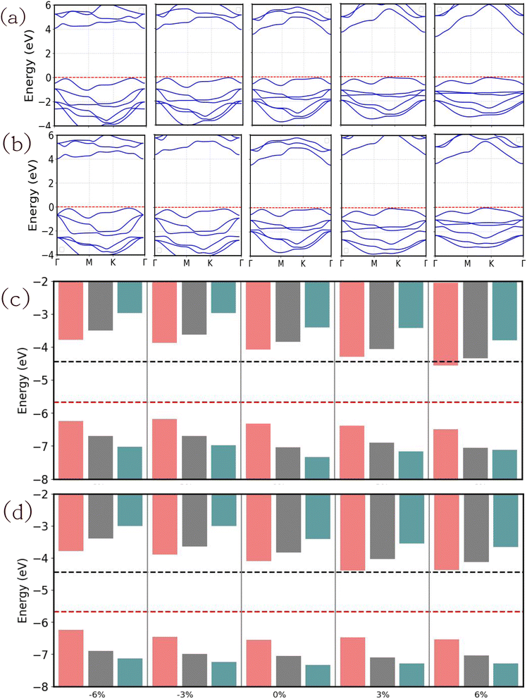 |
| | Fig. 10 The electronic band structure and band alignment of SnIBr (a) and (c) and SnICl (b) and (d) JLs under biaxial strain. The band structure calculations are performed at the GW level. The band alignment data are obtained by GGA (crimson red), HSE (olive green) and GW (red) level approximations. The black and red lines in (c) and (d) represent water reduction and oxidation potential respectively. | |
Table 6 The calculated band gaps (GGA, HSE, and GW) of biaxially strained SnIBr and SnICl JLs
| Strain (%) |
SnIBr (eV) |
SnICl (eV) |
| GGA |
HSE |
GW |
GGA |
HSE |
GW |
| −6 |
2.45 |
3.19 |
4.15 |
2.71 |
3.50 |
4.13 |
| −3 |
2.31 |
3.08 |
4.01 |
2.58 |
3.35 |
4.03 |
| 0 |
2.24 |
2.99 |
3.63 |
2.47 |
3.23 |
3.92 |
| 3 |
2.09 |
2.84 |
3.34 |
2.25 |
3.06 |
3.74 |
| 6 |
1.93 |
2.71 |
3.32 |
2.17 |
2.92 |
3.63 |
To gain insight into the water redox capacity of strained JLs, the VBM BA and CBM BA need to be compared with water redox potentials. For the calculation of BA positions with respect to the vacuum level, electrostatic potential energy calculations are performed and the corresponding results are presented in Fig. S17. We observed that there is no significant difference between the Δϕ in strained and unstrained JLs so the values for 0% strain are used in the calculation of the overpotential. The vacuum level of all the strained structures is calculated based on the highest electronegative surface and presented in Table S7. It is found that the vacuum level is shifting to higher energy with compressive strain and switching to lower energy with tensile strain, and strained SnIBr and SnICl JLs are presented in Table S7.
Fig. 10(c) and (d) show the BA along with the water redox potentials. By considering all the biaxial strained results, the band gap, CBM and VBM are plotted versus the applied strain (Fig. S16). The GGA, HSE and GW results are found to be showing similar trends. When we compare the BA of biaxially strained JLs, the VBM and CBM BA calculated at different levels of approximations straddle the water redox potential except for the 6% of tensile strain in the SnIBr JL. In most cases we observe a higher overpotential for the water reduction reaction for the GW-level results compared to the GGA and HSE level results. The calculated overpotentials for water reduction (HER) and oxidation (OER) reactions are presented in Table 7. At the GW level of approximation, the highest overpotential for the water reduction reaction is 1.77 eV for SnIBr and 1.79 eV for SnICl JLs. This result is obtained for 6% compressive strain. On the other hand, tensile strain gradually decreases the overpotential. The higher the overpotential, the higher the energy provided by the charge carriers for the water reduction reaction under the light-on conditions. From our results, we found that the compressive strain is helping the water reduction reaction to be spontaneous, as it is providing more energy for the reaction to proceed. In the case of overpotential calculated for the OER, the overpotential is increasing with tensile strain in the SnIBr JLs. In SnICl JLs, only a small reduction in overpotential was observed with tensile strain in both the GGA and GW results. However, reduction in the overpotential is observed with compressive strain in both JLs using GGA, HSE and GW levels of approximations.
Table 7 The calculated overpotential of biaxially strained SnIBr and SnICl JLs. The overpotentials were calculated with respect to the standard hydrogen electrode potential at pH = 0
| Strain (%) |
Overpotential-HER (eV) |
Overpotential-OER (eV) |
| SnIBr |
SnICl |
SnIBr |
SnICl |
| GGA |
HSE |
GW |
GGA |
HSE |
GW |
GGA |
HSE |
GW |
GGA |
HSE |
GW |
| −6 |
0.86 |
1.14 |
1.67 |
1.14 |
1.40 |
1.79 |
1.80 |
2.26 |
2.59 |
1.80 |
2.46 |
2.70 |
| −3 |
0.77 |
1.03 |
1.68 |
0.91 |
1.15 |
1.58 |
1.75 |
2.26 |
2.54 |
2.03 |
2.56 |
2.81 |
| 0 |
0.57 |
0.80 |
1.24 |
0.71 |
0.97 |
1.39 |
1.88 |
2.40 |
2.60 |
2.11 |
2.62 |
2.89 |
| 3 |
0.36 |
0.59 |
1.22 |
0.56 |
0.76 |
1.25 |
1.94 |
2.46 |
2.73 |
2.04 |
2.66 |
2.85 |
| 6 |
0.09 |
0.31 |
0.85 |
0.43 |
0.65 |
1.14 |
2.05 |
2.61 |
2.68 |
2.10 |
2.60 |
2.85 |
Furthermore, we have calculated the total energy and adsorption energy of molecule-substrate complexes on the strained JLs and presented them in Tables S8 and 8 respectively. The adsorption energy of H on all the strained JLs is in the range of 1.45 eV to 2.13 eV. In the oxidation reaction steps of SnIBr, we noticed that the adsorption energy of oxygen is lower than that of OH molecules. But the OOH* adsorption energy is higher than that of the adsorption energy of oxygen. This behaviour occurs at all strain values considered. In the case of the SnICl oxidation reaction process, the adsorption energy of OH is found to be the highest. Again, this trend is observed for all the strain values investigated. Further steps of O* formation and OOH* formation possess lower adsorption energy.
Table 8 The calculated adsorption energy of H*, O*, OH*, and OOH* substrate-molecule complexes formed on the biaxially strained JLs
| SnIBr (eV) |
SnICl (eV) |
| Structure |
H* |
OH* |
O* |
OOH* |
Structure |
H* |
OH* |
O* |
OOH* |
| SnIBr (−6) |
1.45 |
2.86 |
1.64 |
3.48 |
SnICl (−6) |
1.52 |
3.30 |
1.23 |
0.80 |
| SnIBr (−3) |
1.47 |
2.72 |
1.80 |
3.53 |
SnICl (−3) |
1.85 |
3.34 |
1.53 |
0.85 |
| SnIBr (0) |
2.05 |
3.13 |
1.50 |
3.53 |
SnICl (0) |
2.12 |
3.42 |
1.22 |
0.73 |
| SnIBr (3) |
2.13 |
2.70 |
1.86 |
3.48 |
SnICl (3) |
1.96 |
3.24 |
1.15 |
0.82 |
| SnIBr (6) |
1.81 |
2.25 |
2.07 |
3.50 |
SnICl (6) |
1.53 |
1.98 |
1.88 |
0.82 |
Based on the adsorption energies the GFE profile under light-off conditions was determined. Fig. S19(a) and (b) demonstrate that both tensile and compressive strain may reduce the GFE value of the Volmer step of the reduction reaction. Also, the oxidation reaction can be positively influenced by strain (Fig. S19(c) and (d)). Fig. 11 shows the results for light-on conditions (pH = 0) using the GW level data for the overpotential (see Table 6). In the case of SnIBr, 3% and 6% compressive strain decreases the GFE change in the H* formation step of the reduction reaction to −0.01 and −0.12 eV, respectively (Fig. 11(a)). In the case of the SnICl JL, we observed that all the strained conditions helped decrease the GFE change in the Volmer reaction, with the lowest GFE change of −0.07 eV for 6% compressive strain (Fig. 11(b)), i.e. the Volmer step is exergonic or spontaneous. Fig. 11(c) and (d) depict the results for the oxidation reaction. In the case of both SnIBr and SnICl JLs, the compressive and tensile strain may reduce the GFE change of the rate-determining step significantly. In the case of SnIBr and SnICl JLs, 6% strain reduced the RDS to −0.15 eV and −0.53 eV, which helps the reaction to be spontaneous. We have also studied the water oxidation reaction at pH equal to 7 and 14 (Fig. S20). In general, there is a decrease in the GFE change in all the water oxidation reaction steps compared to the unstrained JL. The results show that at higher pH values the GFE of the reaction steps is more negative than that for pH = 0 in both the JLs. This enhances the spontaneity of reaction steps and of the whole OER. In the case of the SnIBr JL at pH = 14 (alkaline conditions) the whole OER is spontaneous even under all compressive and tensile strain conditions considered.
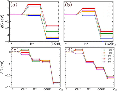 |
| | Fig. 11 The GFE profile of water reduction and oxidation reactions of the biaxially strained SnIBr (a) and (c) and SnICl (b) and (d) JLs under the light-on conditions and at pH = 0. | |
3.9.2 Uniaxial strain engineering.
To further study the effect of uniaxial strain we have applied 6% compressive and tensile strain along the x and y axes of the JLs. The energetic stability of the strained JLs is confirmed by the obtained negative formation energy results (Table S9). It is observed that the 6% uniaxially strained JLs show an energy difference of 0.04 eV compared to unstrained JLs. So, we found that the strained JLs maintain reasonable structural configuration without any breaking of the bonds.
The GGA and HSE band structures of the uniaxially strained JLs are presented in Fig. S21. In all the strained cases, the JLs are showing an indirect band gap. The CBM of uniaxially strained JLs are at the Γ point and the VBM vary in between K and Γ points. Fig. 12(a) and (b) show more accurate GW band structures in which band dispersion matches with the GGA and HSE level results depicted in Fig. S21. The calculated band gap in all the uniaxially strained JLs is presented in Table 9. At the GW level approximation, the highest band gap obtained for SnIBr JL is 3.91 eV and SnICl is 4.00 eV, for 6% compressive strain along the x-axis. To study the water reduction capacity of uniaxially strained JLs, band alignment needs to be studied. The electrostatic potential energy calculated for the uniaxially strained JLs is presented in Fig. S22. Similarly to the case of biaxial strain, the value of Δϕ for strained JLs is nearly equal to that for the unstrained JLs, so that value is used in the calculation of the HER overpotential viaeqn (32). The calculated CBM and VBM positions of all the uniaxially strained JLs with respect to vacuum levels are presented in Table S10. It is found that CBM and VBM of all the structures straddle the water reduction and oxidation potential at pH equal to zero, see Fig. 12(c) and (d). Therefore, for all strain values considered the water redox reaction is possible. As expected, the GW level BA provides higher overpotential compared to GGA and HSE level calculations. Also, from Table 10, it is clear that the compressive strain along the y-axis provides the largest overpotential (1.59) in SnIBr. In contrast, the uniaxial compressive strain along the x-axis provides the largest overpotential (1.55 eV) in SnICl. We have also studied the overpotentials corresponding to the water oxidation reaction in the uniaxially strained JLs and presented them in Table 10.
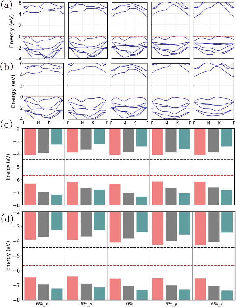 |
| | Fig. 12 The electronic band structure and band alignment of SnIBr (a) and (c) and SnICl (b) and (d) JLs calculated under the 6% of tensile and compressive strain along the x and y directions. The electronic band structure calculations are performed at the GW level. The band alignment of all the strained JLs is calculated using GGA (blue), HSE (green) and GW (red) levels of approximations. The black and red lines in the illustration of the band alignment diagram represent water reduction and oxidation potential respectively. | |
Table 9 The calculated band gaps (GGA, HSE, and GW) of uniaxially strained SnIBr and SnICl JLs
| Strain (%) |
SnIBr (eV) |
SnICl (eV) |
| GGA |
HSE |
GW |
GGA |
HSE |
GW |
| -6x |
2.23 |
2.98 |
3.91 |
2.26 |
3.25 |
4.00 |
| -6y |
2.34 |
2.97 |
3.71 |
2.48 |
3.22 |
3.88 |
| 0 |
2.24 |
2.99 |
3.63 |
2.47 |
3.23 |
3.92 |
| 6y |
2.07 |
2.76 |
3.45 |
2.26 |
3.01 |
3.74 |
| 6x |
2.07 |
2.74 |
3.41 |
2.26 |
2.99 |
3.94 |
Table 10 The calculated overpotentials of uniaxially strained SnIBr and SnICl JLs. The overpotentials were calculated with respect to the standard hydrogen electrode potential at pH = 0
| Strain (%) |
Overpotential-HER (eV) |
Overpotential-OER (eV) |
| SnIBr |
SnICl |
SnIBr |
SnICl |
| GGA |
HSE |
GW |
GGA |
HSE |
GW |
GGA |
HSE |
GW |
GGA |
HSE |
GW |
| −6x |
0.57 |
0.76 |
1.41 |
0.90 |
1.08 |
1.55 |
1.87 |
2.52 |
2.74 |
2.04 |
2.53 |
2.81 |
| −6y |
0.79 |
0.99 |
1.59 |
0.87 |
1.10 |
1.53 |
1.76 |
2.19 |
2.34 |
1.97 |
2.48 |
2.71 |
| 0 |
0.57 |
0.80 |
1.24 |
0.71 |
0.97 |
1.39 |
1.88 |
2.40 |
2.60 |
2.11 |
2.62 |
2.89 |
| 6y |
0.56 |
0.78 |
1.02 |
0.53 |
0.78 |
1.23 |
1.72 |
2.19 |
2.64 |
2.09 |
2.59 |
2.87 |
| 6x |
0.55 |
0.78 |
1.23 |
0.52 |
0.73 |
1.37 |
1.73 |
2.17 |
2.39 |
2.10 |
2.62 |
2.93 |
The total energy and adsorption energy of substrate-molecule complexes formed by the adsorption of H, O, OH, and OOH molecules on the uniaxially strained JLs are presented in Tables S11 and 11 respectively. The adsorption energy of the H on uniaxially strained JLs is in the range of 2–3 eV in both SnIX JLs. In the case of water oxidation reaction steps in SnIBr strained structures, OH* and OOH* possess higher adsorption energy than O* whereas in SnICl OH* has the highest adsorption energy. Using the adsorption energy data we determined the GFE profile of water reduction and oxidation reactions. Fig. S23 shows the results for light-off conditions and pH = 0 and Fig. 13 shows those for the light-on case and pH = 0. In the light-off case, compressive strain along the x (zig–zag) or y (arm chair) directions slightly reduces the GFE change of water reduction in SnIBr (Fig. S23(a)) while for SnICl such a decrease is found under all strain conditions (Fig. S23(b)). Under light-off conditions, the RDS of water oxidation in SnIBr decreases with tensile stress (Fig. S23(c)) whereas for SnICl a reduction is obtained under all considered strain conditions (Fig. S23(d)). Using the overpotential data given in Table 10 the results for light-on conditions were obtained and are shown (for pH = 0) in Fig. 13. It is found that compressive (tensile) strain reduces (increases) the GFE value of the Volmer reaction step. The largest reduction was shown by the 6% compressive strain along x directions, i.e., 0.66 eV and 0.58 eV for SnIBr and SnICl JLs respectively. In the case of the water oxidation reaction at pH equal to zero, we found that the 6% tensile strain can reduce the GFE change of the different steps significantly (Fig. 13(c) and (d)). In the case of SnIBr, positive GFE is found in OH* and OOH* formation steps. The data for SnICl show negative GFE values for all steps. Along with this, we have also studied the water oxidation reactions under higher pH conditions (pH = 7 and 14, see Fig. S24). Under alkaline conditions for certain strain values all reaction steps in SnIBr and SnICl are exergonic, i.e. the GFE change is negative, e.g. for 6% tensile strain.
Table 11 The calculated adsorption energies of H*, O*, OH*, and OOH* substrate-molecule complexes formed on the uniaxially strained JLs
| SnIBr (eV) |
SnICl (eV) |
| Structure |
H* |
OH* |
O* |
OOH* |
Structure |
H* |
OH* |
O* |
OOH* |
| SnIBr (−6x) |
2.07 |
3.06 |
1.62 |
3.37 |
SnICl(−6x) |
2.13 |
3.28 |
1.48 |
0.71 |
| SnIBr (−6y) |
2.38 |
3.43 |
1.57 |
3.50 |
SnICl(−6y) |
2.41 |
2.60 |
2.48 |
0.73 |
| SnIBr |
2.05 |
3.13 |
1.50 |
3.53 |
SnICl |
2.12 |
3.42 |
1.22 |
0.73 |
| SnIBr (6y) |
2.61 |
2.29 |
2.56 |
3.52 |
SnICl(6y) |
2.33 |
3.07 |
0.91 |
1.48 |
| SnIBr (6x) |
2.33 |
3.18 |
1.40 |
3.50 |
SnICl(6x) |
2.13 |
2.36 |
0.89 |
1.95 |
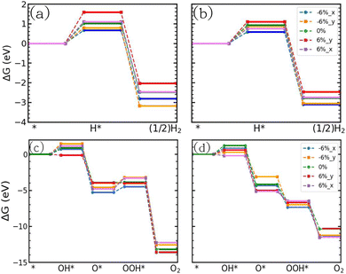 |
| | Fig. 13 The GFE profile of the uniaxially strained SnIBr (a) and (c) and SnICl (b) and (d) JLs under the light-on conditions and at pH = 0. | |
3.10 The reaction rate determining steps (RDSs) under light-on conditions: summary of previous GW level results
In the case of the HER the H* formation is the rate-determining step, whereas for the OER the OH* formation is the rate-determining step. The compilation of all previous data on the corresponding RDS is depicted in Fig. 14. Most beneficial for OWS is the situation where both the HER and OER should ideally consist of two or four GFE downhill steps, which means spontaneous reactions (see e.g.Fig. 11). But also cases with positive GFE change in the RDS close to zero are advantageous. In Fig. 14(a), the plot corresponding to the bare JLs shows that the water reduction reaction is more favorable at pH = 0 or under acidic conditions, whereas the GFE change increases with higher pH values. The RDS of the water oxidation reaction is close to zero at pH = 14 or under alkaline conditions in the case of the SnIBr JL. In SnICl, the RDS is close to zero under acidic conditions and less than zero under higher pH conditions. In the bare JL, it is hard to find the pH condition with the RDS of both the reduction and oxidation reaction steps to be close to zero. In the case of JLs with the iodine monovacancy, Fig. 14(b), the RDS of the water reduction reaction is less than zero in both the JLs, indicating that the reduction reaction is thermodynamically favorable under all pH conditions. We assume that the iodine vacancy will not affect the oxidation reactions performed on the opposite surface (X surface). So, we consider that the RDS in the water oxidation reaction is similar to that of bare JLs. Hence, we found that the water redox reactions are most favorable at a pH = 14 for the SnIBr JL. In the case of the SnICl JL, pH ≥ 1.3, reduction and oxidation reactions are spontaneous. The RDS of the water oxidation reaction step is close to zero at a lower pH value of less than 1.3. Furthermore, Fig. 14(c)–(f) shows the variation of the RDS with pH in the biaxially strained JLs. In all the biaxially strained JLs, the RDS corresponding to the water reduction reaction is low under lower pH conditions and increases with an increase in the pH value. It is observed that the 3% and 6% compressive strain brings the RDS of water reduction and oxidation reactions close to zero under neutral conditions (pH = 7) in both SnIBr and SnICl JLs. In the JL with tensile strain, the RDS of the water reduction reaction is hardly favorable. At the same time, the RDS of the water oxidation reaction step is negative at pH higher than 6.7. In a lower pH range of less than 6.7, GFE change in the water oxidation reaction is close to zero. The GFE change of the RDS of the HER in SnICl is less than zero for 6% compressive strain and pH = 0, but the value becomes positive at higher pH. At tensile strain the value is still higher. In SnICl water oxidation is most favourable at 6% tensile strain. For other strain values the GFE change of the RDS is lowest at high pH. Fig. 14 shows that 6% compressive strain and a pH value of around 7 are most beneficial for OWS, for both JLs. Finally, the RDS variation with strain in the uniaxially strained JL is presented in Fig. 14(g)–(j). It is found that the RDS of water reduction reactions is positive and larger at higher pH values in all cases. In the case of the water oxidation reaction, the RDS is close to or less than zero under alkaline conditions. Therefore in the case of uniaxial strain engineering, it is hard to find pH conditions where both the reduction and oxidation reactions are favourable. The case of 6% compressive strain along the x direction and pH close to zero leads to the smallest positive GFE of the RDS of both reduction and oxidation reactions.
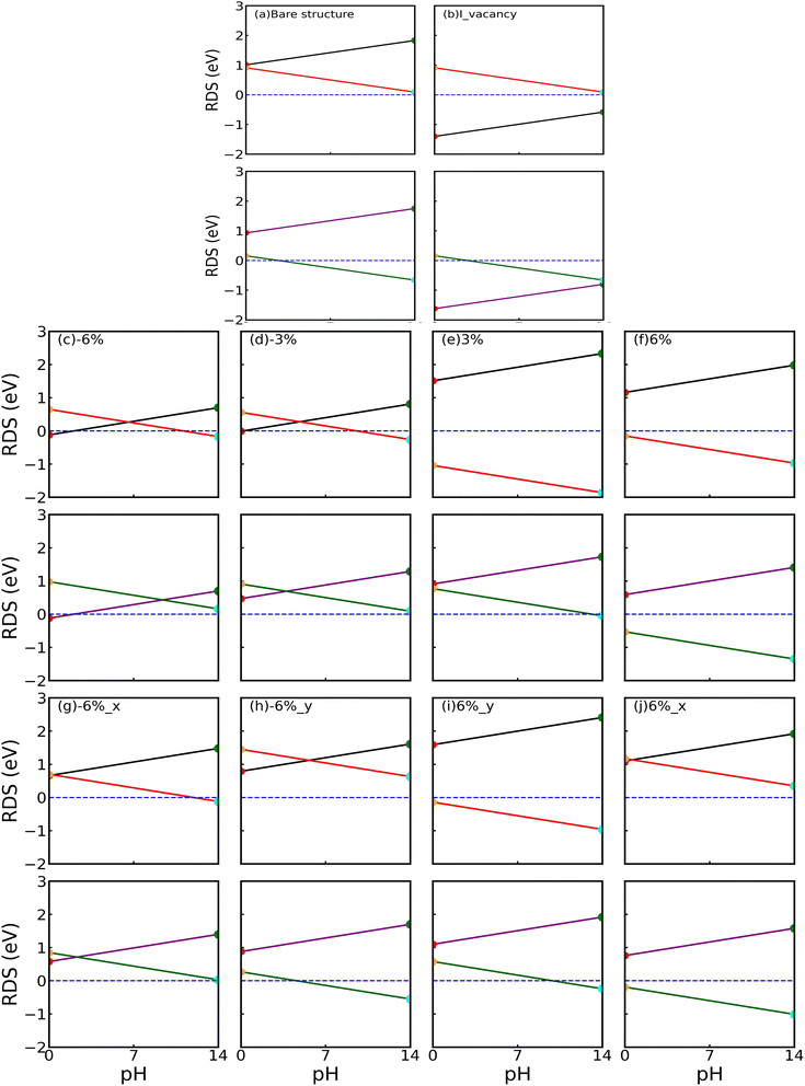 |
| | Fig. 14 The variation of the reaction rate determining step (RDS) in water reduction and oxidation with pH for the bare JL (a), the JL with an iodine monovacancy (b), and biaxial ((c)–(f)) and uniaxial ((g)–(j)) strain. In the case of SnIBr, black and red colours are chosen for water reduction and oxidation reactions, whereas in SnICl green and violet colours are used for water reduction and oxidation reactions. The data shown in the diagrams were obtained using the GW level approximation. | |
4 Solar to hydrogen efficiency
The overall photocatalytic mechanism involves the conversion of solar energy into hydrogen energy with the help of a photocatalyst. According to the study done by Yang et al.,80 the STH efficiency of the designed photocatalyst is defined as the product of solar light absorption efficiency and the carrier utilization efficiency.Here the ηabs and ηcu are the light absorption efficiency and carrier utilization efficiency respectively. ηabs can be calculated as follows:| | 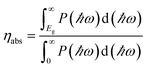 | (36) |
The numerator represents the power density of light absorbed by the photocatalyst. The denominator is the total power density of solar spectra obtained on the earth's surface. For this, we consider P(ℏω) as the air mass 1.5 G solar energy flux at the photon energy ℏω. We considered Eg as the band gap of the strained and strain-free JLs (here, we consider GGA level band gap). Later, the carrier utilization efficiency was calculated as
| | 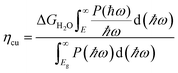 | (37) |
ΔG(H2O) is the free energy of water splitting (1.23 eV). The numerator represents the product of the free energy of water splitting and the effective photocurrent density. The photon energy (E) is different for each system and can be selected from the conditions below:
Here,
χ(
H2) and
χ(
O2) are the overpotentials noted in the rate-determining step of water reduction and oxidation reactions respectively. The calculated light absorption efficiency, carrier utilization efficiency, and overall solar to hydrogen efficiency are presented in Table S12. We noticed that the light utilisation efficiency is showing an inverse relation with the bandgap. We have noticed an increase in light utilization efficiency with the decrease in the bandgap, whereas the carrier utilization efficiency depends on HER and OER overpotentials. Our result shows that the STH efficiency of SnIBr is high (11.12%) compared to that of the SnICl (7.14%) JL. We have also noticed that the compressive strain decreases the STH efficiency in both SnIBr and SnICl monolayers, while tensile strain enhances the STH efficiency of the JLs. The highest STH efficiency is shown by the 6 percent biaxial strain in both SnIBr and SnICl JLs, which is reported to be 15.71% and 12.62% respectively. In the case of uniaxial strain, the 6 percent tensile strain along the
x and
y directions helps attain an STH efficiency of 15.01% in the SnIBr JL. In the SnICl JL, the uniaxial strain along
x and
y directions helps attain STH efficiencies of 10.70% and 10.14%. The obtained solar to hydrogen efficiency is in the same range as that of the other previously reported 2D materials.
81,82
5 Conclusion
In summary, we have successfully designed lead-free SnIX (X = Br/Cl) JLs. The negative formation energy and the absence of imaginary modes in phonon spectra indicate that the material is energetically and thermodynamically stable. Furthermore, the low temperature and energy fluctuation during the AIMD simulation indicate that the material is stable under ambient conditions. The elastic constants calculated from the energy strain curve suggest that the designed structures are mechanically stable. This analysis also reveals the high flexibility of the JLs. The phase diagrams suggest that the SnIX JLs can be formed from the parent structures SnI2 or SnX2 using advanced CVD techniques by varying the chemical potential of halide elements.
The calculated band gap shows that SnIX JLs mainly show UV light absorption. We found that the calculated effective mass of the electrons (0.08 m0: SnIBr and 0.09 m0: SnICl) of JLs is comparable with that of other 2D JLs. The large mobility of electrons along the zig–zag direction is obtained to be 2.88 × 103 cm2 V−1 s−1 for SnIBr and 1.55 × 103 cm2 V−1 s−1 for SnICl and is found to be about one order higher than that of previously reported 2D materials. The notable difference in electron and hole mobility leads to an enhanced lifetime of charge carriers and reduces the possibility of charge recombination. Computationally expensive GW-BSE calculation reveals that the electron–hole interactions are spatially spread in the K–Γ–M region in the reciprocal lattice. The exciton binding energy of SnIBr is 0.60 eV which is smaller than the corresponding data for other 2D materials. On the other hand, the value for SnICl (0.97 eV) is comparable to those data. The exciton binding energies determined using the classical Mott–Wannier model are somewhat smaller than the results of GW-BSE calculations.
The calculated electrostatic potential along the out-of-plane direction suggests that the recombination of photoexcited electrons and holes is mitigated by the potential drop (0.21 eV in SnIBr and 0.36 eV in SnICl). The BA calculated for both the JLs at GGA, HSE, and GW level approximations satisfies the conditions required for the water-splitting reactions. Under light-off conditions, the GFE change in the water reduction reaction was found to be 2.25 eV for SnIBr and 2.32 eV for SnICl JL. In the case of the oxidation reaction, the largest GFE change was observed for the OH* formation step. This was calculated to be 3.51 eV for SnIBr and 3.05 eV for the SnICl JL. In the light-on case and at pH = 0, the GFE change for the water reduction reaction was reduced to 1.01 eV in SnIBr and 0.93 eV in the SnICl JL. The GFE change in the OH* formation step was reduced to 0.91 eV for SnIBr and 0.16 eV for the SnICl JL. Furthermore, defect and strain engineering helps reduce the RDS in the HER and OER. For JLs with an I vacancy, the RDS of the HER reduces to −0.16 eV in SnIBr and −0.23 eV in the SnICl JL under the light-off conditions. The light-on conditions enhance the spontaneity of the reduction reaction. Under light-on conditions and at pH = 0, the HER becomes spontaneous. Strain may also lead to a reduction of GFE change in the HER. We noticed that the water reduction reaction is favorable with compressive strain and the oxidation reaction may become spontaneous with tensile strain. In SnIBr and at pH = 0, the 3% and 6% biaxial compressive strain effectively reduces the GFE change in the HER to −0.01 eV and −0.12 eV, and in SnICl at pH = 0, 6% compressive strain leads to a GFE change of −0.07 eV. In these three cases, the HER proceeds spontaneously. In the case of uniaxially strained JLs, we found the lowest (but endergonic) GFE for the Volmer step of the HER for 6% compressive strain. At a given strain, the RDS of the OER decreases with the pH value, both for biaxial and uniaxial strain. In SnIBr and SnICl, the OER is spontaneous at 3% and 6% biaxial tensile strain, either for high pH values or within the whole pH range. The 6% tensile strain along the armchair direction makes the OER in SnIBr spontaneous, whereas the spontaneous OER in SnICl is found for the same strain in the zig–zag direction. The compilation of the obtained data shows that the RDS of the HER is smallest at pH = 0 and can be further reduced by defect (I monovacancy) and compressive strain engineering. On the other hand, the RDS data for the OER are smallest at pH = 14 and can be further diminished by tensile strain. Under compressive strain and at medium pH values there are optimum conditions for OWS (i.e. for both the HER and OER) with the RDS close to 0 eV.
Overall, the wide band gap, low exciton binding energy, substantially high electron mobility, built-in electric field, and favorable band alignment with respect to the water redox potential make the SnIX JLs potential candidates for water-splitting hydrogen production. By applying defect and strain engineering these JLs may show spontaneous HER and OER within certain ranges of the pH value of water. From the calculated STH efficiency also, we found that the tensile strain improves the efficiency of the SnIX JLs drastically. The biaxial tensile strain could enhance the STH efficiency of SnIBr from 11.12% to 15.71%, while in SnICl, the STH efficiency raised from 7.14% to 14.49%.
Conflicts of interest
There are no conflicts to declare.
Data availability
Structural, electronic, and optical properties of the parent SnX2 structures are given in the SI, together with additional data on phonon spectra, phonon DOS, atom resolved electronic DOS, etc. of the SnIX Janus layers. See DOI: https://doi.org/10.1039/d5ta04079e.
Acknowledgements
Dr D. Murali is thankful to the Department of Science and Technology – Science and Engineering Research Board (DST-SERB) for financial support (CRG/2022/006778).
Notes and references
- W. Zhen, X. Ning, B. Yang, Y. Wu, Z. Li and G. Lu, Appl. Catal., B, 2018, 221, 243–257 CrossRef CAS.
- K. T. Møller, T. R. Jensen, E. Akiba and H.-w. Li, Prog. Nat. Sci.: Mater. Int., 2017, 27, 34–40 CrossRef.
- F. Dawood, M. Anda and G. Shafiullah, Int. J. Hydrogen Energy, 2020, 45, 3847–3869 CrossRef CAS.
- L. X. Chen, Z. W. Chen, Y. Zhang, C. C. Yang and Q. Jiang, Appl. Catal., B, 2019, 258, 118012 CrossRef CAS.
- P. Zhou, I. Navid, Y. Ma, Y. Xiao, P. Wang, Z. Ye, B. Zhou, K. Sun and Z. Mi, Nature, 2023, 613, 66–70 CrossRef CAS PubMed.
- V. Kumaravel, S. Mathew, J. Bartlett and S. C. Pillai, Appl. Catal., B, 2019, 244, 1021–1064 CrossRef CAS.
- C. Bie, L. Wang and J. Yu, Chem, 2022, 8, 1567–1574 CAS.
- H. Jiang, L. Zheng, Z. Liu and X. Wang, InfoMat, 2020, 2, 1077–1094 CrossRef CAS.
- Y. Li, S. Wu, J. Zheng, Y.-K. Peng, D. Prabhakaran, R. A. Taylor and S. C. E. Tsang, Mater. Today, 2020, 41, 34–43 CrossRef CAS.
- D. Xie, F. Yang, X. Qiu, Y. Hu, Y. Sun, S. He and X. Wang, Phys. B, 2024, 684, 415953 CrossRef CAS.
- A. Chaves, J. Azadani, H. Alsalman, D. Da Costa, R. Frisenda, A. Chaves, S. Song, Y. Kim, D. He, J. Zhou, A. Castellanos-Gomez, F. Peeters, Z. Liu, C. Hinkle, S.-H. Oh, P. Ye, S. Koester, Y. H. Lee, P. Avouris and T. Low, npj 2D Mater. Appl., 2020, 4, 29 CrossRef CAS.
- M. Bernardi, M. Palummo and J. C. Grossman, Nano Lett., 2013, 13, 3664–3670 CAS.
- J. Yang, M. Zheng, Y. Wu, F. Le Goualher, J. Di, T. Salim, Y. Deng, C. Zhu, S. Guo, B. Tang, S. Li and Z. Liu, Appl. Catal., B, 2024, 343, 123478 CAS.
- S. Lei, L. Ge, Z. Liu, S. Najmaei, G. Shi, G. You, J. Lou, R. Vajtai and P. M. Ajayan, Nano Lett., 2013, 13, 2777–2781 CrossRef CAS PubMed.
- S. Sucharitakul, N. J. Goble, U. R. Kumar, R. Sankar, Z. A. Bogorad, F.-C. Chou, Y.-T. Chen and X. P. A. Gao, Nano Lett., 2015, 15, 3815–3819 CrossRef CAS PubMed.
- D. Liu, A. Barbar, T. Najam, M. S. Javed, J. Shen, P. Tsiakaras and X. Cai, Appl. Catal., B, 2021, 297, 120389 CrossRef CAS.
- T. Mueller and E. Malic, npj 2D Mater. Appl., 2018, 2, 29 CrossRef.
- H. S. Waheed, H. Ullah, M. Waqas Iqbal and Y.-H. Shin, Optik, 2022, 271, 170071 CrossRef CAS.
- A. Reserbat-Plantey, I. Epstein, I. Torre, A. T. Costa, P. A. D. Gonçalves, N. A. Mortensen, M. Polini, J. C. W. Song, N. M. R. Peres and F. H. L. Koppens, ACS Photonics, 2021, 8, 85–101 CrossRef CAS.
- I. Choudhuri, P. Bhauriyal and B. Pathak, Chem. Mater., 2019, 31, 8260–8285 CrossRef CAS.
- W. Shi, K. Fan and Z. Wang, Phys. Chem. Chem. Phys., 2018, 20, 29423–29429 RSC.
- C. O. Xueling Lei and K. Huang, Appl. Surf. Sci., 2021, 537, 147919 CrossRef.
- T. Zhao, J. Chen, X. Wang and M. Yao, Appl. Surf. Sci., 2021, 545, 148968 CrossRef CAS.
- X. Gao, Y. Shen, J. Liu, L. Lv, M. Zhou, Z. Zhou, Y. P. Feng and L. Shen, J. Mater. Chem. C, 2021, 9, 15026–15033 RSC.
- M. Xie, Y. Shang, X. Li, Y. Da and X. Liu, ACS Appl. Nano Mater., 2023, 6, 10569–10580 CrossRef CAS.
- Y. Bai, Q. Zhang, N. Xu, K. Deng and E. Kan, Appl. Surf. Sci., 2019, 478, 522–531 CrossRef CAS.
- J.-X. Guo, S.-Y. Wu, G.-J. Zhang, L. Yan, J.-G. Hu and X.-Y. Li, J. Colloid Interface Sci., 2022, 616, 177–188 CrossRef CAS PubMed.
- J.-H. Lin, H. Zhang, X.-L. Cheng and Y. Miyamoto, Phys. Rev. B: Condens. Matter Mater. Phys., 2017, 96, 035438 CrossRef.
- V. V. Thanh, D. V. Truong and N. Tuan Hung, ACS Appl. Energy Mater., 2023, 6, 910–919 CrossRef CAS.
- T. Zhang, Y. Liang, H. Guo, H. Fan and X. Tian, Appl. Surf. Sci., 2022, 579, 152017 CrossRef CAS.
- Y. Zhao, B. Zhang and J. Lin, Appl. Surf. Sci., 2023, 621, 156883 CrossRef CAS.
- M. R. Ebrahimi, A. Banjafar and T. Vazifehshenas, Phys. B, 2024, 683, 415891 CrossRef CAS.
- P. Chauhan, J. Singh and A. Kumar, J. Mater. Chem. A, 2024, 12, 16129–16142 RSC.
- Y. Mao, Z. Yao, J. Yuan and X. Chang, Appl. Surf. Sci., 2022, 598, 153633 CrossRef CAS.
- X. Zhang, Y. Cui, L. Sun, M. Li, J. Du and Y. Huang, J. Mater. Chem. C, 2019, 7, 13203–13210 RSC.
- R. Silva, R. Barbosa, R. Mançano, N. Durães, R. Pontes, R. Miwa, A. Fazzio and J. E. Padilha, ACS Appl. Nano Mater., 2019, 2, 890–897 CrossRef.
- D. Mehta, Y. Naik, N. Modi, P. Parmar and P. Thakor, Comput. Mater. Sci., 2024, 236, 112861 CrossRef CAS.
- C. Chowdhury, S. Karmakar and A. Datta, J. Phys. Chem. C, 2017, 121, 7615–7624 CrossRef CAS.
- Y. Wu, C.-H. Yang, H.-N. Zhang, L.-H. Zhu, X.-Y. Wang, Y.-Q. Li, S.-Y. Zhu and X.-C. Wang, Appl. Surf. Sci., 2022, 589, 152999 CrossRef CAS.
- M. Vallinayagam, A. E. Sudheer, S. A. Aravindh, D. Murali, N. Raja, R. Katta, M. Posselt and M. Zschornak, J. Phys. Chem. C, 2023, 127, 17029–17038 CrossRef CAS.
- X. Yan, Z. Chen, Y. Yue, R. Chai, H. Ou, Y. Li and G. Yang, Appl. Catal., B, 2025, 360, 124527 CrossRef CAS.
- X. Huang, M. Wan, F. Liu, H.-z. Song and M. Yang, J. Phys. Chem. C, 2023, 127, 22105–22111 CrossRef CAS.
- Q. Yang, D. Wang, Z.-Y. Zeng, H.-Y. Geng and X.-R. Chen, Phys. Rev. B, 2024, 109, 035411 CrossRef CAS.
- A. E. Sudheer, G. Tejaswini, M. Posselt and D. Murali, Comput. Mater. Sci., 2024, 243, 113123 CrossRef CAS.
- Y. Sun and K. Liu, J. Appl. Phys., 2018, 125, 082402 CrossRef.
- Z. Lin, B. R. Carvalho, E. Kahn, R. Lv, R. Rao, H. Terrones, M. A. Pimenta and M. Terrones, 2D Mat., 2016, 3, 022002 CrossRef.
- G. Tejaswini, A. E. Sudheer, M. Vallinayagam, M. Posselt, M. Zschornak, S. Maniprakash and D. Murali, Phys. Chem. Chem. Phys., 2024, 26, 29339–29350 RSC.
- T. Tang, Z. Wang and J. Guan, Chin. J. Catal., 2022, 43, 636–678 CrossRef CAS.
- D. D. Vo, T. V. Vu, S. Al-Qaisi, H. D. Tong, T. Le, C. V. Nguyen, H. V. Phuc, H. L. Luong, H. R. Jappor, M. M. Obeid and N. N. Hieu, Superlattices Microstruct., 2020, 147, 106683 CrossRef CAS.
- Z. Liu, B. Wang and C. Cazorla, ACS Sustainable Chem. Eng., 2022, 10, 16924–16934 CrossRef CAS.
- G. Guo, S. Tan, G. Guo and Z. Xie, Colloids Surf., A, 2023, 659, 130782 CrossRef CAS.
- G. Kresse and J. Furthmüller, Phys. Rev. B: Condens. Matter Mater. Phys., 1996, 54, 11169 CrossRef CAS PubMed.
- G. Kresse and J. Furthmüller, Comput. Mater. Sci., 1996, 6, 15–50 CrossRef CAS.
- P. E. Blochl, Phys. Rev. B: Condens. Matter Mater. Phys., 1994, 50, 17953 CrossRef PubMed.
- G. Kresse and D. Joubert, Phys. Rev. B: Condens. Matter Mater. Phys., 1999, 59, 1758–1775 CrossRef CAS.
- J. P. Perdew, K. Burke and M. Ernzerhof, Phys. Rev. Lett., 1996, 77, 3865 CrossRef CAS PubMed.
- H. J. Monkhorst and J. D. Pack, Phys. Rev. B, 1976, 13, 5188 CrossRef.
- S. Grimme, J. Comput. Chem., 2006, 27, 1787–1799 CrossRef CAS PubMed.
- J. Heyd, G. E. Scuseria and M. Ernzerhof, J. Chem. Phys., 2003, 118, 8207–8215 CrossRef CAS.
- A. Togo, L. Chaput, T. Tadano and I. Tanaka, J. Phys.: Condens. Matter, 2023, 35, 353001 CrossRef CAS PubMed.
- A. Togo, J. Phys. Soc. Jpn., 2023, 92, 012001 CrossRef.
- E. Salpeter and H. Bethe, Phys. Rev. B, 1951, 84, 1232–1242 CrossRef.
- A. Mostofi, J. Yates, Y.-S. Lee, I. Souza, D. Vanderbilt and N. Marzari, Comput. Phys. Commun., 2008, 185, 685–699 CrossRef.
- Q. Yuan, F. Zheng, Z. Shi, Q. Li, Y. Lv, Y. Chen, P. Zhang and S.-C. Li, Adv. Sci., 2021, 8, 2100009 CrossRef CAS PubMed.
- D. Akinwande, C. J. Brennan, J. S. Bunch, P. Egberts, J. R. Felts, H. Gao, R. Huang, J.-S. Kim, T. Li, Y. Li, K. M. Liechti, N. Lu, H. S. Park, E. J. Reed, P. Wang, B. I. Yakobson, T. Zhang, Y.-W. Zhang, Y. Zhou and Y. Zhu, Extreme Mechanics Letters, 2017, 13, 42–77 CrossRef.
- S.-D. Guo, Phys. Chem. Chem. Phys., 2018, 20, 7236–7242 RSC.
- N. Raja, D. Murali, S. V. M. Satyanarayana and M. Posselt, RSC Adv., 2019, 9, 34158–34165 RSC.
- P. Erhart and K. Albe, J. Appl. Phys., 2008, 104, 044315 CrossRef.
- P. Cudazzo, C. Attaccalite, I. V. Tokatly and A. Rubio, Phys. Rev. Lett., 2010, 104, 226804 CrossRef PubMed.
- L. Ju, M. Bie, X. Tang, J. Shang and L. Kou, ACS Appl. Mater. Interfaces, 2020, 12, 29335–29343 CAS.
- R.-I. Biega, Y. Chen, M. R. Filip and L. Leppert, Nano Lett., 2023, 23, 8155–8161 CrossRef CAS PubMed.
- P. Wang, Y. Zong, H. Liu, H. Wen, H.-X. Deng, Z. Wei, H.-B. Wu and J.-B. Xia, J. Phys. Chem. C, 2020, 124, 23832–23838 CrossRef CAS.
- H. L. Zhuang and R. G. Hennig, Phys. Rev. B: Condens. Matter Mater. Phys., 2013, 88, 115314 CrossRef.
- E. Skúlason, G. S. Karlberg, J. Rossmeisl, T. Bligaard, J. Greeley, H. Jónsson and J. K. Nørskov, Phys. Chem. Chem. Phys., 2007, 9, 3241–3250 RSC.
- N.-T. Suen, S.-F. Hung, Q. Quan, N. Zhang, Y.-J. Xu and H. M. Chen, Chem. Soc. Rev., 2017, 46, 337–365 RSC.
- J. K. Nørskov, J. Rossmeisl, A. Logadottir, L. Lindqvist, J. R. Kitchin, T. Bligaard and H. Jónsson, J. Phys. Chem. B, 2004, 108, 17886–17892 CrossRef PubMed.
- J. Nørskov, T. Bligaard, J. Rossmeisl and C. Christensen, Nat. Chem., 2009, 1, 37–46 CrossRef PubMed.
- J. Xiong, J. Di, J. Xia, W. Zhu and H. Li, Adv. Funct. Mater., 2018, 28, 1801983 CrossRef.
- J. Wang, S. U. Rehman, Z. Tariq, X. Zhang, J. Zheng, F. K. Butt and C. Li, Sol. Energy Mater. Sol. Cells, 2021, 230, 111258 CrossRef CAS.
- C.-F. Fu, J. Sun, Q. Luo, X. Li, W. Hu and J. Yang, Nano Lett., 2018, 18, 6312–6317 CrossRef CAS PubMed.
- P. Jamdagni, A. Kumar, S. Srivastava, R. Pandey and K. Tankeshwar, Phys. Chem. Chem. Phys., 2022, 24, 22289–22297 RSC.
- J. Singh and A. Kumar, J. Mater. Chem. C, 2023, 11, 1173–1183 RSC.
|
| This journal is © The Royal Society of Chemistry 2025 |
Click here to see how this site uses Cookies. View our privacy policy here. 
 *a
*a
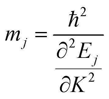
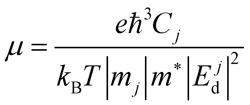
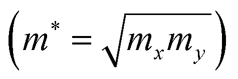 . T is the temperature and e is the charge of the electron, while kB is Boltzmann's constant.

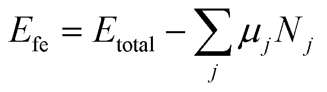


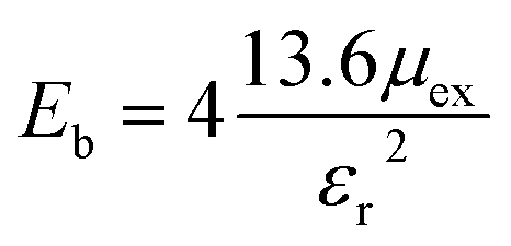
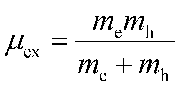 . The εr is the calculated dielectric constant of the material. The excitonic binding energy is calculated to be 0.57 eV in the SnIBr monolayer and 0.77 eV in the SnICl monolayer. This is smaller than that obtained from the GW-BSE spectra. Differences between the GW and MW results were also reported for other unsymmetrical 2D structures.71,72 Within the Mott–Wannier model, the excitonic radius is calculated using
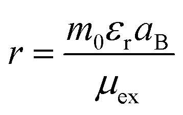
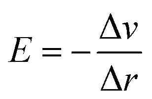


 and
and  are calculated VBM and CBM, without shifting the Fermi level to zero. Evacuum is the vacuum level corresponding to the more electronegative sublayer in the JLs. i.e., the Br layer in SnIBr and the Cl layer in SnICl JL. We have calculated the VBM and CBM band edge levels using DFT with GGA and HSE exchange-correlation functionals and with the single-shot GW method. We found that the vacuum level is insensitive to the exchange-correlation functional in the case of SnIX JLs. Based on the assumption that the vacuum level is not changed in the many-body perturbation theory, we have calculated the BA of SnIX structures. The BA diagram is depicted in Fig. 6 and the related data are presented in Table S4. To study the water redox ability of the JLs, BA needs to be compared with water reduction and oxidation potentials. The water redox potentials are pH-dependent based on the equation shown73 (in eV):
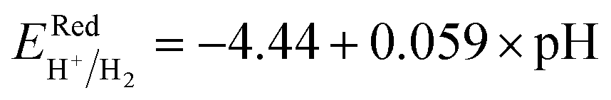
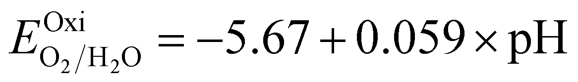


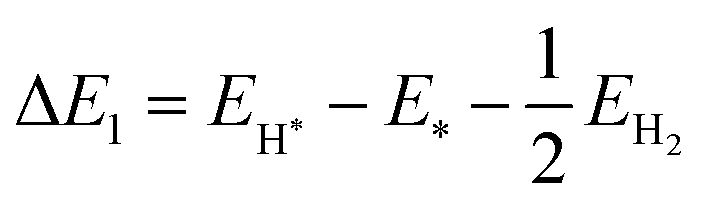
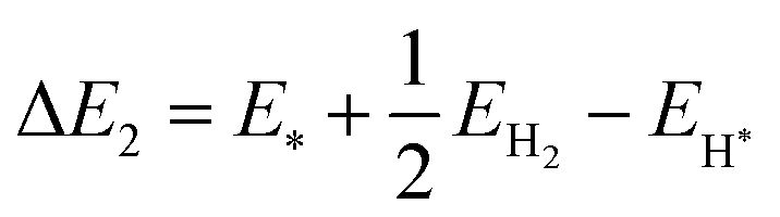
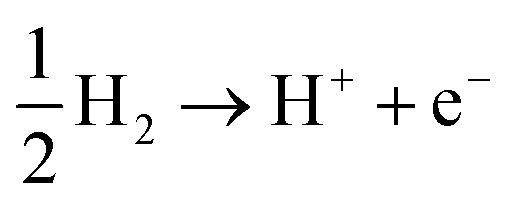 has zero reaction energy under standard temperature and pressure conditions. Therefore the GFE before and after the reaction is the same under light-off conditions, see e.g.Fig. 8(a) and (b). The relaxed geometry of the H-substrate complex is presented in Fig. 7. The hydrogen is adsorbed on the top of the I atom with a bond distance of 1.65 Å on both SnIBr and SnICl JLs. From SnIBr JL, a 0.92 e charge is transferred to the hydrogen atom, whereas 0.93 e charge is transferred from the SnICl JL to the hydrogen atom during the hydrogen adsorption reaction step. By analysing the geometry after the structural relaxation, we have noticed a small local distortion on the H-adsorbed I atom. However, the overall structure is found to be quite stable. Similarly, the adsorption energy of OH, O, and OOH on the substrate during the oxidation reaction and energy change in the O2 desorption step, see eqn (21)–(24), are
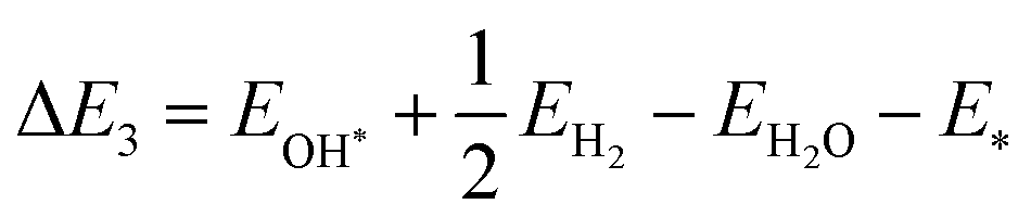
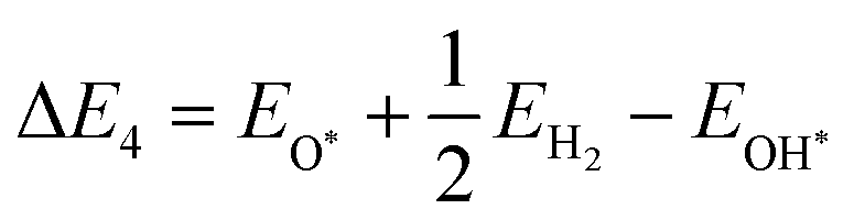
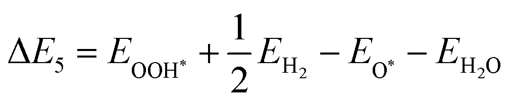
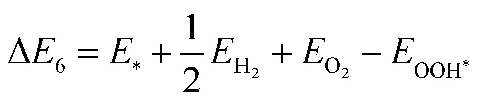


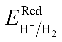 and
and 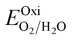 are water reduction and oxidation potentials which depend on different pH conditions, see eqn (16) and (17), and Δϕ is the difference in the vacuum level of top and bottom sublayers in the JLs which is obtained from Fig. 6(a) and (c).