
 Open Access Article
 This Open Access Article is licensed under a Creative Commons Attribution-Non Commercial 3.0 Unported Licence
Thermoelectric performance boost by chemical order in epitaxial L21 (100) and (110) oriented undoped Fe2VAl thin films: an experimental and theoretical study†
José María
Domínguez-Vázquez
 a,
Olga
Caballero-Calero
a,
Ketan
Lohani
a,
José J.
Plata
b,
Antonio M.
Marquez
b,
Cristina V.
Manzano
a,
Miguel Ángel
Tenaguillo
a,
Hiromichi
Ohta
c,
Alfonso
Cebollada
a,
Andres
Conca
*a and
Marisol
Martín-González
a
a,
Olga
Caballero-Calero
a,
Ketan
Lohani
a,
José J.
Plata
b,
Antonio M.
Marquez
b,
Cristina V.
Manzano
a,
Miguel Ángel
Tenaguillo
a,
Hiromichi
Ohta
c,
Alfonso
Cebollada
a,
Andres
Conca
*a and
Marisol
Martín-González
a
aInstituto de Micro y Nanotecnología, IMN-CNM, CSIC (CEI UAM+CSIC, ), Isaac Newton 8, E-28760 Tres Cantos, Madrid, Spain. E-mail: andres.conca@csic.es
bDepartamento de Química Física, Facultad de Química, Universidad de Sevilla, 41012, Seville, Spain
cResearch Institute for Electronic Science, Hokkaido University, N20W10, Kita, Sapporo, 001-0020, Japan
First published on 3rd July 2025
Abstract
This study demonstrates the direct correlation between the presence of the L21 ordered phase and the significant enhancement in the thermoelectric performance of Fe2VAl thin films deposited on MgO and Al2O3 substrates at temperatures varying between room temperature and 950 °C. We employ both experimental techniques and computational modeling to analyze the influence of crystallographic orientation and deposition temperature on the thermoelectric properties, including the Seebeck coefficient, electrical conductivity, and thermal conductivity. Our findings indicate that the presence of the L21 phase significantly enhances the power factor (PF) and figure of merit (zT), surpassing previously reported values for both bulk and thin film forms of Fe2VAl, achieving a PF of 480 μW m−1 K−2 and a zT of 0.025.
Introduction
Thermoelectric materials have the unique ability to convert thermal gradients into electrical voltage, enabling direct energy conversion between heat and electricity. This property positions them as key players in addressing the global energy crisis, particularly in waste heat recovery and energy-efficient cooling applications across various industrial sectors. By capturing wasted thermal energy, they can significantly improve the overall efficiency of energy systems. Additionally, these materials offer a sustainable, low-maintenance solution for powering Internet of Things (IoT) devices, wearable technologies, and biomedical sensors. The efficiency of thermoelectric energy conversion is governed by the dimensionless figure of merit, zT, which is defined as zT = S2σT/κ, where S is the Seebeck coefficient, σ is the electrical conductivity, T is the temperature, and κ is the thermal conductivity. Thus, high-performing thermoelectric materials are those that exhibit a high S and σ, while maintaining a low κ. Bismuth telluride (Bi2Te3),1,2 lead telluride (PbTe)3,4 and selenides such as SnSe,5,6 Ag2Se7 and Cu2Se8 have been extensively studied as the best-performing thermoelectric materials for different temperature applications. However, challenges related to cost, toxicity, and the scarcity of some of these materials limit their practical application. In recent years, Heusler alloys—specifically, half-Heusler XYZ9–11 and full-Heusler X2YZ12–15 compounds—have emerged as promising alternatives due to their tunable semiconducting properties and earth-abundant, eco-friendly compositions. Notably, Fe2VAl,16–19 a full-Heusler alloy, has attracted significant attention for its potential thermoelectric applications. Fe2VAl exhibits relatively high power factors (PF = S2σ) and can be tailored to p- or n-type conductivity through stoichiometric variations or doping with abundant elements, such as Ti and Cr20,21 for p-type and W, Si, or Ta22–25 for n-type.Recent breakthrough research26 has demonstrated that Fe2VAl exhibits exceptional thermoelectric properties at the Anderson transition, a quantum phase transition from localized to mobile electron states, where conditions for ideal thermoelectric performance are met. Complementary to this, other studies have proved that electronic band engineering,27 off-stoichiometric doping18 or self-substitution28,29 can significantly enhance the power factor (PF = S2·σ) and the figure of merit (zT). Our approach focusses on the chemical order of the phase, representing a distinct yet complementary strategy to these advances.
Fe2VAl possesses a cubic structure with varying degrees of chemical order that strongly influence its electronic band structure and thermoelectric properties. These different structures are illustrated in the left column of Fig. 1: the chemically disordered cubic phase, A2, which has all three elements occupying lattice positions at random; the B2 phase, where Al and V occupy positions indistinctively; and finally, the fully ordered L21 phase, where each element atom occupy univocally specific lattice sites. These three phases, characterized by increasing chemical order, endow the material with specific band structure features and, as a consequence, different thermoelectric properties. This is shown in the right column of Fig. 1, where theoretically calculated band structures and DOS are shown for A2, B2 and L21 phases, respectively. In the same figure, the right indicates the theoretically expected values of electrical conductivity and Seebeck coefficient for B2 and L21 structures. As can be seen, chemical order causes the opening of an energy gap in the band structure (which becomes more defined with increasing degrees of the mentioned chemical order), a change in the band curvature and a shift in the slope of the density of states (DOS). Consequently, these changes affect the thermoelectric properties and, according to theoretical calculations, chemical order leads to an increase in the Seebeck coefficient, ultimately showing the largest values when the L21 structure is considered. It is worth mentioning that although other properties such as electrical or thermal conductivity seem to evolve towards worsening thermoelectric efficiency with greater chemical ordering, the presented calculations predict that this increase in the Seebeck coefficient makes the L21 structure the one that reaches the highest value of zT.
 | ||
| Fig. 1 Crystalline structures of Fe2VAl for different degrees of chemical order: A2 (a), B2 (b) and L21 (c), along with their corresponding band structure, DOS and simulated electrical conductivity and Seebeck coefficient (for the B2 and L21 structures), for charge carrier concentrations and crystallite sizes in the range of 5 × 1020 cm−3 and 40 nm, respectively. | ||
Conceptually, preparing thermoelectric materials in thin film form offers numerous advantages over bulk materials due to reduced thermal conductivity at the nanoscale, their applicability as covering functional layers or their use of small amounts of material. Fe2VAl thin films, in particular, have demonstrated enhanced thermoelectric performance, especially when grown via sputtering—a scalable, industry-friendly deposition method—although most studies focus on polycrystalline films. However, while epitaxial films, with long-range crystalline coherence, provide an ideal platform for studying the intrinsic thermoelectric response of model systems and allow for more accurate comparisons with theoretical predictions, investigations into epitaxial or single-oriented thin films and their thermoelectric properties remain scarce.
In this work, we govern the appearance of the previously mentioned cubic phases in Heusler alloy Fe2VAl (100) and (110) oriented thin films grown by sputtering from stoichiometric targets and experimentally study their corresponding thermoelectric properties. Chemical order and crystalline orientation are simply controlled by adequate selection of deposition temperature, Tdep, and substrate orientation. In our case, MgO (100) and Al2O3 (11−20) substrates promote the growth in the (100) and (110) directions, respectively, and allow us to obtain the desired cubic phase with a controllable degree of chemical order. Specifically, we demonstrate the relevance of growing at high Tdep in promoting the L21 phase, for which our results show a notable enhancement in PF and zT values compared to previously reported Fe2VAl thin films, underscoring the potential of these materials for practical thermoelectric applications.
Growth and characterization of Fe2VAl thin films
A summary of the crystalline phases determined by X-ray diffraction measurements for the studied films is shown in Fig. 2 (full details in the ESI†). Generally speaking, for both substrates, increasing Tdep leads to a higher degree of crystallinity. Films grown below 350 °C are nanocrystalline or amorphous in nature, as no diffraction peaks are observed for them. For Tdep between 350 and below 850 °C, the highest ordered structure present in the films is B2 for films deposited over MgO and, either B2 or A2 for films deposited over Al2O3 (depending on Tdep). In this range of Tdep, films grown on MgO are epitaxial, (100) oriented, due to the favourable cube-on-cube symmetry matching, while those grown on Al2O3 are polycrystalline. Finally, for Tdep higher than or equal to 850 °C in both substrates, the L21 phase is detected. In this last range of Tdep, films grown over MgO are epitaxial but, due to the lower symmetry of the Al2O3 (11![[2 with combining macron]](https://www.rsc.org/images/entities/char_0032_0304.gif) 0) face, films deposited on this substrate are only (110) textured or single-oriented, but not epitaxial, lacking in-plane crystalline coherence. The complete X-ray diffraction (XRD) data and characterization can be found in the ESI.†
0) face, films deposited on this substrate are only (110) textured or single-oriented, but not epitaxial, lacking in-plane crystalline coherence. The complete X-ray diffraction (XRD) data and characterization can be found in the ESI.†
 | ||
| Fig. 2 Highest chemically ordered crystalline structures and type of growth obtained for ranges of deposition temperature (Tdep) between RT and 950 °C for the two different substrates used in this work (MgO and Al2O3). Two main ranges are highlighted: in blue, 350–850 °C, with B2 or A2 as the highest chemically ordered structure present, and in yellow 850–950 °C, where L21 presence is observed. | ||
As it is seen in Fig. 1, theoretical calculations predict strong effects of the chemical order on both band structure and thermoelectric properties of the compound. To experimentally confirm this correlation, in Fig. 3 we show the Tdep dependence of the normalized intensity of the (1 1 1) XRD peak, proving L21 presence in the film, along with the measured Seebeck coefficient, conductivity and Power Factor (PF). On the one hand, a twofold increase in the Seebeck coefficient (positive for all samples, and therefore p-type) is observed as Tdep increases between 350 and 800 °C, with quite a linear behaviour. For 850 °C and above, along with a gradual increase in the (111) reflection in the XRD analysis, and thus the presence of L21 phase, the Seebeck coefficient experiences another twofold increase.
 | ||
| Fig. 3 Thermoelectric properties and L21 presence as a function of deposition temperature (Tdep) of Fe2VAl thin films. (a) Relative intensity of the (1 1 1) X-ray diffraction peak with respect to the (2 2 0) peak, (b) Seebeck coefficient, (c) conductivity and (d) PF were plotted highlighting the samples with L21 presence in yellow and those with B2 or A2 structures in blue. Along with data points, a guide to the eye for the evolution of the distinct properties was included (dashed line). | ||
On the other hand, the electrical conductivity experiences a continuous, gradual decrease as Tdep increases from 350 °C to 950 °C, probably due to the rougher, more pronouncedly agglomerated morphology in the films observed via AFM and SEM (discussed later), which may enhance charge carrier scattering at higher Tdep. Interestingly, this decrease saturates when the L21 phase is obtained, and therefore, band structure effects on the electrical conductivity associated with the presence of this ordered phase cannot be disregarded.
Combining the Seebeck coefficient and electrical conductivity measurements, we observe two distinct regions in the power factor dependence on deposition temperature (Tdep). In the absence of the L21 phase (lower Tdep): the PF shows a linear, gradual increase with Tdep. Once the L21 phase is present (higher Tdep), an abrupt change in the slope of PF vs. Tdep is observed, with a steeper increase. Although minor variations exist between substrates, the overall trend of increasing PF with higher Tdep is consistent for both MgO and Al2O3 substrates. The similarity in PF values between films grown in different crystalline orientations ((100) on MgO and (110) on Al2O3) suggests isotropic electronic transport properties in Fe2VAl. This isotropy is further confirmed by in-plane rotation measurements, where the Seebeck coefficient remains constant regardless of the thermal gradient direction relative to the crystalline axis.
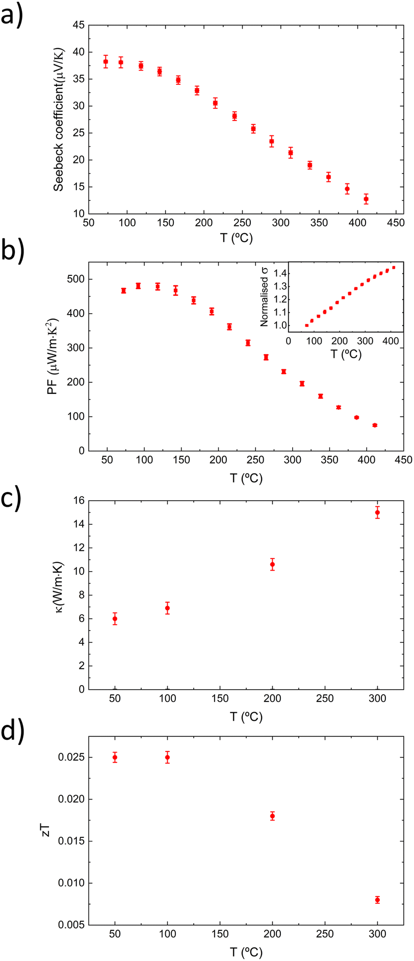
Thermal conductivity (κ) measurements by TDTR at room temperature for films deposited on MgO yield values of 4.4 ± 0.2 W m−1 K−1 for the B2 phase (Tdep = 350 °C) and 4.6 ± 0.2 W m−1 K−1 for the L21 phase (Tdep = 950 °C). Interestingly, these κ values are within the experimental error of each other, indicating that the structural ordering primarily affects the power factor rather than the thermal conductivity. Given that Fe2VAl is a cubic phase and theoretically isotropic, we can calculate the figure of merit (zT) for both phases: B2 phase: zT = 0.004 and L21 phase: zT = 0.016. This represents a fourfold increase in zT for the L21 phase compared to the B2 phase, highlighting the significant impact of structural ordering on the thermoelectric performance (mainly in the power factor) of Fe2VAl thin films. Fig. 4 shows the evolution with temperature of the Seebeck coefficient, PF, normalised σ, κ and zT of a Fe2VAl thin film with L21 order (deposited at 900 °C over MgO). The plot shows a gradual decrease in the Seebeck coefficient with increasing temperature and, therefore, a decrease in the power factor. A complementary increase in the electrical and thermal conductivity is observed. The inset included in Fig. 4(b), showing the temperature dependence of normalised σ, shows a semiconductor-like behaviour, yielding an increasing σ with increasing temperature. The range of temperatures where the maximum of PF and zT is obtained is between 50 and 150 °C, which agrees with previous studies.18,26 The PF peaks at a value of 480 μW m−1 K−2, which corresponds to the largest zT value of 0.025, stable in the mentioned temperature range. The absolute maximal values of zT, together with the value measured at room temperature, are significant since they compare in a very positive manner with those reported in the literature. For a better visualization of this fact, we next make a quantitative comparison between our highest obtained PF values (measured at RT) and those reported in the literature.18,19,22,30–34 For thin film and bulk materials, this is shown in Fig. 5(a), where our obtained PF values are more than twofold of those obtained for other studies. The work by Furuta et al.33 is particularly relevant, as they also reported the epitaxial growth of Fe2VAl films, albeit on MgAl2O4 substrates, which offer a smaller lattice mismatch compared to MgO. However, their PF values were lower, likely due to lower electrical conductivity and Seebeck coefficient. Furuta's films, with a thickness of 1 μm, were significantly thicker than those in this study and exhibited a weaker (111) diffraction peak, suggesting a lower proportion of the L21 phase. Their use of lower deposition temperatures (up to 500 °C) likely limited the chemical ordering and L21 phase development, resulting in reduced thermoelectric performance. In contrast, our study demonstrates the importance of high Tdep for achieving the L21 phase and maximizing thermoelectric performance. This finding is reinforced in Fig. 5(b), where the thermoelectric figure of merit (zT), measured at RT, for Fe2VAl films deposited over MgO at 350 °C and 950 °C is compared with values found in the literature.19,31,33–35 A four-fold increase in the zT value can be seen between these two samples of this work, with the one deposited at a lower temperature (where the L21 phase is absent) in the range of the values found in the literature, while the one deposited at the highest temperature surpasses these values in more than a twofold increase. In Fig. 5(c), the maximum zT (obtained at 50–100 °C) of 0.025 is compared with the maximum zT values obtained in ref. 19, 31 and 33–35, where our reported maximum value surpasses the highest value found in the literature by an almost four-fold increase. Although the values of Furuta et al. and Yamada et al. were measured at room temperature, they do not report values at higher temperatures.
 | ||
| Fig. 4 Temperature dependence of the Seebeck coefficient (a), power factor (b), thermal conductivity (κ) (c) and zT (d) of a Fe2VAl thin film deposited at 900 °C. An inset was included to show the temperature evolution of normalized electrical conductivity. | ||
 | ||
| Fig. 5 Thermoelectric properties of Fe2VAl films from this work compared with bulk and thin film values from the literature. (a) The best values of PF (245 ± 50 and 430 ± 80 μW m−1 K−2) obtained for each orientation are plotted with values obtained from ref. 18, 19, 22, 30–34, (b) zT values at room temperature of Fe2VAl deposited at 350 °C and 950 °C (0.004 ± 0.001 and 0.016 ± 0.004, respectively) are plotted along with values obtained from ref. 19, 31, 33–35 and (c) our maximum value of zT (0.025 ± 0.001) obtained at 50–100 °C is plotted along with maximum values from ref. 19, 31, 33–35. The numbers in brackets along with the names correspond to the studies in the References list. | ||
The zT enhancement is caused by the previously mentioned increase in PF, as the thermal conductivity was found to be almost the same for both films (4.4 ± 0.2 and 4.6 ± 0.2 W m−1 K−1 for Tdep of 350 °C and 950 °C, respectively). This result highlights the importance of L21 ordering for improving the thermoelectric efficiency and the corresponding relevance of Tdep as a growth parameter for Fe2VAl films. Tdep not only influences the nature of the obtained crystalline order (amorphous, textured or epitaxial) but also the final chemical order of the structure (A2, B2 or L21). It affects the growth process, leading to changes in the crystallite and grain sizes, and results in a different film morphology. Different distributions and sizes of crystalline grains may affect the thermoelectric properties, especially thermal conductivity, and therefore, a study of the morphology of the films was conducted. In Fig. 6, SEM micrographs can be seen for three representative Tdep and both substrate cases.
 | ||
| Fig. 6 SEM micrographs of the Fe2VAl thin films grown on MgO and Al2O3. (a–c) Films on MgO at 550 °C, 750 °C, and 850 °C, respectively. (d–f) Films on Al2O3 at the same temperatures. The films with B2/A2 as the highest chemically ordered structure are highlighted in blue, while those with the L21 structure are highlighted in yellow. | ||
The morphology of Fe2VAl films changes drastically with Tdep on both substrates, and the roughness also increases with Tdep. Line profile plots, RMS roughness values and 3D AFM images of these films are shown in the ESI.† For both series of films, a change from a planar to a more granular morphology is observed as Tdep increases. However, differences between the series also appear, due to the different induced grain formation induced by the distinct growth orientations and substrate–film interactions. The enhanced thermoelectric performance observed in our L21 ordered Fe2VAl films presents interesting parallels with the work by Garmroudi et al.26 regarding the Anderson transition in similar materials. While the work by Garmroudi et al. demonstrates optimal thermoelectric conditions when conductive electrons have approximately the same energy at this quantum phase transition, our approach achieves enhancement through structural ordering that modifies the electronic band structure. The thermal conductivity values we report (4.4 ± 0.2 and 4.6 ± 0.2 W m−1 K−1 at room temperature for the B2 and L21 phases, respectively) remain relatively high compared to state-of-the-art thermoelectric materials, suggesting that further optimization through nanostructuring or selective doping could potentially reduce thermal conductivity while preserving the beneficial electronic properties of the L21 phase. From a practical device implementation perspective, our epitaxial thin film approach offers advantages for integration into microelectronic systems where controlled interfaces and structural coherence are critical for reliable performance in energy harvesting applications.
Analysis of thermoelectric behaviour: reconciling theory and experiment
As discussed earlier, the chemical order significantly impacts the band structure of the material, thereby influencing its thermoelectric performance. Key features such as the band gap, band curvature, and density of states are crucial for understanding the measured transport properties. For this reason, it is highly interesting to evaluate the possibility of measuring the energy band gap of this alloy. The estimation of the band gap was carried out by optical methods; therefore, an optically thick (155 nm) sample was deposited at 900 °C over MgO. In Fig. 7 the reflectance spectrum of this sample is plotted along with a Pankove plot (the Tauc plot was also used and obtained the same result). The estimation of the band gap of the sample, as derived from optical measurements, reveals a value of 0.19 ± 0.05 eV. This estimation aligns closely with previous experimental findings, such as those reported by Rai et al.,36 who determined a band gap of approximately 0.2 eV. However, it is slightly lower than the value of 0.27 eV reported by Lue et al.,37 who utilized NMR data in their analysis. The discrepancies in band gap values across different studies can often be attributed to variations in experimental methodologies and sample conditions, including factors such as film thickness, substrate choice, deposition temperature or crystallinity, which can significantly influence optical properties. | ||
| Fig. 7 (a) Reflectance versus photon energy for a 155 nm thick Fe2VAl sample deposited at 900 °C on a MgO (100) substrate. (b) Pankove plot used for the estimation of the band gap (the Tauc method was also used, resulting in the same result: Eg = 0.19 ± 0.05 eV). | ||
The prediction of the electronic structure of Fe2VAl can be challenging and controversial as its experimental characterization. The choice of exchange correlation functional can significantly influence the description of narrow band gap semiconductors when using density functional theory. For instance, General Gradient Approximation (GGA) functionals widely used, such as PBE38 or PBE+U,23 have described L21 Fe2VAl as a semimetal. However, for an effective analysis, we need to consider the role of meta-generalized gradient approximation (meta-GGA) functionals such as mBJ, which typically improve the accuracy of GGAs by accounting for the local kinetic energy density. This has characterized the material as a narrow bandgap semiconductorr.39 Interestingly, these findings complement the work by Garmroudi et al.26 on the quantum phase transition concept in Fe2VAl, where the electronic structure near the Anderson transition creates ideal conditions for thermoelectric performance. Our observation of the enhanced Seebeck coefficient in the L21 phase can be understood as a manifestation of an optimized electronic structure that maximizes the power factor despite modest decreases in electrical conductivity and no change in the thermal conductivity. This mechanism of band structure engineering through chemical ordering represents a broadly applicable approach that could be exploited in other Heusler systems to enhance thermoelectric performance. In this work, the r2SCAN functional has yielded a band gap of 0.18 eV for the L21 ordered phase, which aligns well with the band gaps obtained using the mBJ functional and the experimental evidence reported in this work and previous results reported by Garmroudi et al.26
Tackling the modelling of disorder has led to seemingly contradictory results. While Garmroudi et al.26 experimentally found that disorder reduces the band gap and leads to a metallic band structure for A2,26 computational studies have suggested that disorder can increase the band gap.40 In this work, different degrees of disorder were investigated to monitor the evolution of the band structure and its gap. For low levels of disorder based on V/Al antisite defects, a statistical approach was employed, wherein the band gap of the system was calculated as an ensemble of all possible microstructures. Conversely, B2 and A2 structures were modelled using the Special Quasirandom Structures (SQS) methodology. The calculated band gaps reconcile the previous results. At low concentrations of V/Al antisites, a widening of the band gap is observed, with values of 0.19 and 0.25 eV for 3.125 and 6.25% disorder, respectively. Indeed, the band gap of 0.19 eV at 3.125% of V/Al antisites is very close to the experimental values obtained in this work. However, at higher levels of disorder, the SQS structures used to model the B2 and A2 phases exhibit a reduction in the band gap (Fig. 1), ultimately leading to a metallic structure for the A2 phase.
Obtaining a comprehensive understanding of the thermoelectric performance requires more than just a detailed analysis of the band gap. Other key features, such as band curvature and density of states, are also essential to obtain a complete picture of the thermoelectric behavior. The thermal and transport properties of the L21 phase have been calculated, taking into account the carrier concentration, grain size, and temperature of the synthesized samples (see the ESI†). Cumulative lattice thermal conductivity based on the phonon mean free path demonstrates that the critical variable controlling thermal transport is the grain size (ESI Fig. 18†). While the simulated lattice thermal conductivity (3 and 15 W m−1 K−1 for films with crystallite sizes of 12 and 41 nm, respectively) is in good agreement with experimental results (2.3 and 3.4 W m−1 K−1 for films deposited over MgO at Tdep of 350 and 950 °C, respectively), when grain boundaries are considered in the calculations, the Seebeck coefficient (∼90 μV K−1) and electrical conductivity (∼2200 S cm−1) are slightly overestimated for the L21 phase. However, the calculations capture the trend observed experimentally when disorder is included, predicting an enhancement of the electrical conductivity (∼2400 S cm−1) and a reduction of the Seebeck coefficient (∼80 μV K−1) for the B2 phase. There are different factors that can affect the quantitative agreement between the experiment and theory. It has been previously reported that the methodology applied can overestimate transport properties at high carrier concentration, as is the case here.41 Additionally, other factors such as carrier concentration experimental uncertainties, the coexistence of L21, B2 and A2 phases, epitaxial strain, or texture, which are not included in the model, could play a role in the overall thermoelectric performance.
To understand the behavior of the transport and thermoelectric properties based on the level of disorder, the band structure and density of states of the three phases are compared. A reduction in the band gap when disorder is increased is in good agreement with the enhancement of the electrical conductivity when the deposition temperature is decreased. In the epitaxial films grown on MgO, where the lattice mismatch is smaller, there is a non-monotonous behavior at high Tdep that could be explained by the enlargement of the band gap at small concentrations of V/Al antisites. To explain the large enhancement of the Seebeck coefficient, the slope of the density of states at the edge of the valence band is analyzed for the different levels of disorder. The metallization process due to disorder not only reduces the band gap but also changes the topology of the density of states. The larger the disorder, the flatter the band becomes. In Fig. 8, the edge of the valence band of the L21 and B2 models is plotted, highlighting the position of the Fermi level based on the experimentally measured carrier concentrations for MgO and Al2O3 substrates. The larger slope of the DOS at the L21 phase is in good agreement with the larger Seebeck coefficient obtained experimentally.
 | ||
| Fig. 8 (a) Comparison of the DOS valence band edge for L21 (blue) and B2 (orange) phases. The colored range shows the Fermi energy position based on experimentally determined carrier concentration. | ||
It is important to note that a similar behavior of the band structure with chemical disorder has been calculated by Graf et al.42 for the half-Heusler TiNiSn compound. In their work, the increasing degree of disorder results also in a progressive band-gap closure until a metallic band structure is obtained. Therefore, chemical order can play a significant role in the thermoelectric performance for several half- and full-Heusler compounds.
Conclusions
This study provides compelling evidence that L21 ordered Fe2VAl thin films exhibit superior thermoelectric performance. Thin films grown with Tdep exceeding 850 °C result in significantly improved Seebeck coefficients, thereby enhancing the power factor, with the highest values being 430 ± 80 μW m−1 K−2 and 245 ± 50 μW m−1 K−2 for films on Al2O3 and MgO substrates, respectively. Additionally, thermal conductivity measured by time domain thermoreflectance (TDTR) methods reveals a value of 4.6 ± 0.2 W m−1 K−1 at room temperature for samples deposited on MgO. The optimal zT value of 0.016 was achieved for films deposited at 950 °C, representing a twofold increase compared to previous results in the literature.The substantial variation in the thermoelectric performance of Fe2VAl is closely linked to its electronic structure and the degree of chemical order. Disorder within the crystal structure leads to a semiconductor-to-metal transition, which significantly impacts the transport properties. While the larger band gap of the L21 phase reduces its electrical conductivity, this effect is compensated by the higher Seebeck coefficient. The observed twofold increase in the Seebeck coefficient is attributed to the steepening of the density of states at the valence band edge as the structure transitions from B2 to L21 order.
While other commercially available materials show greater thermoelectric power factors and figures of merit than those shown in this work (PF ∼ 450 μW m−1 K−2, zT ∼ 0.025), for example Bi2Te3 (PF ∼ 5000 μW m−1 K−2, zT ∼ 0.7)2, SnSe (PF ∼ 500 μW m−1 K−2, zT ∼ 0.9)6 or SiGe (PF ∼ 2000 μW m−1 K−2, zT ∼ 1.0),43 this work focusses on the fundamental properties of the undoped alloy. This finding emphasizes the significant potential of Fe2VAl as a promising, earth-abundant, and non-toxic alternative for thermoelectric materials, offering substantial environmental advantages over traditional materials. The work also lays the groundwork for further enhancements via doping with elements such as Ti, W, and Ta, as well as the exploration of structured nanomaterials aimed at reducing thermal conductivity while preserving the favourable electronic characteristics of the L21 phase.
Regarding device integration, challenges persist, particularly concerning the use of monocrystalline substrates such as MgO and Al2O3, which may hinder mass production. However, strategies promoting the deposition of MgO seed layers on more affordable substrates warrant exploration to encourage L21 ordering. The scalability of sputtering methods, utilized in this study, makes them suitable for industrial applications. Moreover, retaining long-term stability through encapsulation or protective layers to prevent corrosion and oxidation is of paramount importance and requires further investigation. Although interdiffusion with electrical contacts could potentially be an issue, this effect is likely minor at the working temperatures anticipated for these films (50–150 °C), although in-depth studies on electrical contacts will further clarify the feasibility of device fabrication. In any case, the contact can be deposited in the sputtering system without breaking the vacuum, which is an advantage compared to other methods.
Ultimately, the scalable sputtering deposition method used in this study offers a pathway for the practical deployment of Fe2VAl in energy harvesting devices, including applications within the internet of things, wearable technologies, and systems for industrial waste heat recovery. These advancements will contribute significantly to global energy efficiency initiatives and to mitigating climate change by reducing reliance on primary energy sources. Nonetheless, it is critical to further investigate the superior thermoelectric performance associated with the L21 phase in bulk material forms, as these findings could potentially amplify the application range and performance of Fe2VAl thermoelectric materials.
Experimental details
Two series of 80 nm thick Fe2VAl thin films were deposited on MgO (1 0 0) and Al2O3 (1 1−2 0) substrates at Tdep ranging from RT to 950 °C. The deposition was carried out in a UHV chamber (base pressure ∼10−9 mbar) utilizing DC magnetron sputtering. A stoichiometric commercial Fe2VAl target (Mateck GmbH) was sputtered at 40 W and 2.5 × 10⁻³ mbar Ar pressure, yielding a deposition rate of 1 nm min−1. Tdep was measured in situ using a calibrated thermocouple located in the sample holder. The structure was evaluated by X-ray Diffraction (XRD) measurements performed on a Bruker D8 Discover four-circle diffractometer with a microfocus X-ray source (IμS) (Cu Kα1) and an Eiger2 2D detector. Rietveld analysis was performed using TOPAS software to obtain lattice parameters and crystallite sizes. Electrical conductivity and charge carrier concentration at RT were measured with a commercial HMS 5500 Hall effect measurement system (Ecopia). Seebeck measurements were carried out with a lab-made system in the in-plane direction at RT. For Seebeck and power factor measurements with varying temperature, a commercial Linseis LSR-3 system was used.The thermal conductivity was measured in the out-of-plane direction using the time-domain thermo-reflectance (TDTR) method at various temperatures, utilizing the front/front configuration. The measurements were performed with a PicoTR system (PicoTherm), employing a pump and probe laser with wavelengths of 1550 nm and 750 nm, respectively. Both lasers feature a pulse duration of 0.5 ps, and the laser pulses were applied to the film (after depositing a thin Pt layer on top of it) within a time interval of 50 ns. From these measurements, the thermal diffusivity is obtained, and from that and knowing the different parameters of the film and substrate (density of 6.584 g cm−3 and heat capacity of 527 J kg−1 K), the thermal conductivity can be calculated. These measurements were conducted at the Research Institute for Electronic Science (RIES) at Hokkaido University in Japan. Details of the PicoTR system have been described elsewhere.44–46 For estimating the lattice thermal conductivity, the electrical contribution of the lattice thermal conductivity was calculated using the Wiedemann–Franz law47 with a Lorenz number of 2.44 × 10⁻⁸ V2 K−2 and subtracted from the total thermal conductivity measured by TDTR.
Morphological characterization was carried out via a FEI Verios 460 Scanning Electron Microscope (SEM). Atomic Force Microscopy (AFM) micrographs were obtained for two representative films of each series and are shown in the ESI.†
The band gap was determined through the optical reflectance using Pankove and Tauc approaches. The reflectance was measured in the mid-IR range (from 2.5 to 17 μm) with a Fourier Transform Infrared (FT-IR) spectrophotometer from PerkinElmer (Spectrum 3).
Computational details
Ground-state structures were fully relaxed using the VASP package48 and projector-augmented wave potentials.49 Due to the band gap underestimation by the GGA functional, energies and band structure were calculated with the r2SCAN functional proposed by Furness et al.50 Core and valence electrons were selected following the standards proposed by Calderon et al.51 The plane-wave basis set expansion had a kinetic energy cut-off of 500 eV, which is 25% above the standard value for the chosen PAW potentials, to reduce Pulay stress errors. Meshes of 432 and 1024 k-points per reciprocal atom were used to accurately describe the minimum of the potential energy surface and the ground state wavefunction, respectively. Geometry and lattice vectors were fully relaxed until forces on each atom were below 10−7 eV Å−1. The wave-function was considered converged when the energy difference between consecutive electronic steps was less than 10−9 eV, including an additional support grid for the evaluation of the augmentation charges to reduce noise in the forces.To explore the V/Al antisite disorder in the Fe2VAl bulk, we constructed a 2 × 2 × 2 periodic model containing 128 atoms. We simulated low antisite defect concentrations of 3.125% and 6.25%, with one and two antisite defects, respectively. All possible vacancy distributions were analyzed using the SOD package52 and the high-throughput framework, DisorderNML.53 The average properties of the disordered material were calculated by considering the contribution of each supercell to the partition function. The B2 and A2 phases were modelled using Special Quasirandom Structures (SQS54) as implemented in the ICET code.55 SQS cells provide a good approximation of random alloys, as their cluster vectors closely resemble those of truly random alloys. To compare the electronic structure of the L21 phase and SQS structures, band structure unfolding56 was performed using the easyunfold code.57
Lattice thermal conductivity was calculated by combining the hiPhive58 and ShengBTE59 packages using the hiPhive wrapper.60 The force constants were obtained using 20 3 × 3 × 3 supercells, using the conventional cell as the unit cell. Antisite disorder was modelled using the Tamura model,61 which includes an isotopic or elastic scattering term that accounts for mass disorder. The influence of grain size on lattice thermal conductivity was considered by determining the cumulative thermal conductivities based on phonon mean free paths; the value of κ for a specific particle size L is estimated by summing the contributions from all mean free paths up to L. Electronic transport properties were computed using the AMSET code,62 which solves the Boltzmann transport equation using the Onsager coefficients to predict electronic transport properties, with the wave function from a DFT calculation as the main input. Scattering rates were calculated for each temperature, doping concentration, band, and k-point, including scattering due to deformation potentials, polar optical phonons, and ionized impurities. More details on the methodology used to compute electronic transport properties can be found in previous studies.41,63
Data availability
All the data supporting the findings will be available at https://digital.csic.es/ after publication. Additional data are available from the corresponding author upon reasonable request.Author contributions
J. M. Domínguez-Vázquez, A. Conca, A. Cebollada, O. Caballero-Calero and M. Martín-González designed the experiment and outlined the work plan for this research, J. M. Domínguez-Vázquez, A. Conca and A. Cebollada contributed to the film growth, J. M. Domínguez-Vázquez, A. Conca, A. Cebollada and K. Lohani participated in the X-ray diffraction measurements and analysis, O. Caballero-Calero conducted the thermoelectric property measurements, M. A. Tenaguillo and H. Ohta carried out and coordinated the thermoreflectance thermal conductivity measurements, J. J. Plata and A. M. Márquez performed the computational simulations and subsequent analysis, and C. V. Manzano measured the optical band gap. AFM and SEM imaging were carried out by the MiNa services at IMN. M. Martín-González participated in the discussion with all the co-authors to achieve the final conclusions and secured financial support for A. Conca, M. A. Tenagillo, and J. M. Dominguez-Vazquez to carry out this work. Finally, J. M. Domínguez-Vázquez, A. Conca, O. Caballero-Calero, A. Cebollada, K. Lohani, J. J. Plata, C. V. Manzano and M. Martín-González contributed to the drafting of the manuscript.Conflicts of interest
There are no conflicts to declare.Acknowledgements
The authors would also like to acknowledge the service from the MiNa Laboratory at IMN, and its funding from EU (FEDER, FSE), MCIN/AEI/10.13039/501100011033 and Next Generation EU/PRTR (EQC2021-006944-P). This work was funded by projects THERMHEUS grant TED2021-131746B-I00 funded by MICIU/AEI/10.13039/501100011033 and by the “European Union NextGenerationEU/PRTR” and ERC Adv. POWERbyU grant agreements ID: 101052603 funded by European Research Council (ERC), and grant PID2022-138063OB-I00 funded by MICIU/AEI/10.13039/501100011033 and by FEDER, UE. We gratefully acknowledge the computer resources at Lusitania (Cenits-COMPUTAEX), Red Española de Supercomputación, RES (QHS-2023-1-0028) and Albaicín (Centro de Servicios de Informática y Redes de Comunicaciones – CSIRC, Universidad de Granada).References
- C. V. Manzano, B. Abad, M. Muñoz Rojo, Y. R. Koh, S. L. Hodson, A. M. Lopez Martinez, X. Xu, A. Shakouri, T. D. Sands, T. Borca-Tasciuc and M. Martin-Gonzalez, Sci. Rep., 2016, 6, 19129 CrossRef CAS PubMed.
- I. T. Witting, T. C. Chasapis, F. Ricci, M. Peters, N. A. Heinz, G. Hautier and G. J. Snyder, Adv. Electron. Mater., 2019, 5, 1800904 CrossRef.
- T. Fu, X. Yue, H. Wu, C. Fu, T. Zhu, X. Liu, L. Hu, P. Ying, J. He and X. Zhao, J. Materiomics, 2016, 2, 141–149 CrossRef.
- A. D. Lalonde, Y. Pei, H. Wang and G. Jeffrey Snyder, Mater. Today, 2011, 14, 526–532 CrossRef CAS.
- M. Jin, J. Jiang, R. Li, X. Wang, Y. Chen, R. Zhang and Y. Chen, Mater. Res. Bull., 2019, 114, 156–160 CrossRef CAS.
- C. Zhou, Y. K. Lee, Y. Yu, S. Byun, Z. Z. Luo, H. Lee, B. Ge, Y. L. Lee, X. Chen, J. Y. Lee, O. Cojocaru-Mirédin, H. Chang, J. Im, S. P. Cho, M. Wuttig, V. P. Dravid, M. G. Kanatzidis and I. Chung, Nat. Mater., 2021, 20, 1378–1384 CrossRef CAS PubMed.
- J. A. Perez-Taborda, O. Caballero-Calero, L. Vera-Londono, F. Briones and M. Martin-Gonzalez, Adv. Energy Mater., 2018, 8, 1702024 CrossRef.
- J. A. Perez-Taborda, L. Vera, O. Caballero-Calero, E. O. Lopez, J. J. Romero, D. G. Stroppa, F. Briones and M. Martin-Gonzalez, Adv. Mater. Technol., 2017, 2, 1700012 CrossRef.
- H. Hohl, A. P. Ramirez, C. Goldmann, G. Ernst, B. Wölfing and E. Bucher, J. Phys.: Condens. Matter, 1999, 11, 1697–1709 CrossRef CAS.
- Y. Lei, Y. Li, L. Xu, J. Yang, R. Wan and H. Long, J. Alloys Compd., 2016, 660, 166–170 CrossRef CAS.
- C. Yu, T. J. Zhu, R. Z. Shi, Y. Zhang, X. B. Zhao and J. He, Acta Mater., 2009, 57, 2757–2764 CrossRef CAS.
- T. Graf, C. Felser and S. S. P. Parkin, Prog. Solid State Chem., 2011, 39, 1–50 CrossRef CAS.
- Y. Kurosaki, S. Yabuuchi, A. Nishide, N. Fukatani and J. Hayakawa, Appl. Phys. Express, 2022, 15, 085502 CrossRef CAS.
- Y. Shimanuki, S. Yamada, A. Masago, T. Ishibe, K. Kudo, Y. Nakamura and K. Hamaya, Phys. Rev. B, 2020, 102, 054203 CrossRef CAS.
- H. Li, K. Hayashi, Z. Huang, H. Takeuchi, G. Kanno, J.-F. Li and Y. Miyazaki, J. Materiomics, 2024, 10, 511–519 CrossRef.
- H. Okamura, J. Kawahara, T. Nanba, S. Kimura, K. Soda, U. Mizutani, Y. Nishino, M. Kato, I. Shimoyama, H. Miura, K. Fukui, K. Nakagawa, H. Nakagawa and T. Kinoshita, Phys. Rev. Lett., 2000, 84, 3674 CrossRef CAS PubMed.
- Y. Kawaharada, K. Kurosaki and S. Yamanaka, J. Alloys Compd., 2003, 352, 48–51 CrossRef CAS.
- Y. Nishino, H. Kato, M. Kato and U. Mizutani, Phys. Rev. B: Condens. Matter Mater. Phys., 2001, 63, 233303 CrossRef.
- S. Yamada, K. Kudo, R. Okuhata, J. Chikada, Y. Nakamura and K. Hamaya, Appl. Phys. Express, 2017, 10, 115802 CrossRef.
- H. Matsuura, Y. Nishino, U. Mizutani and S. Asano, J. Jpn. Inst. Met., 2002, 66, 767–771 CrossRef CAS.
- N. Reumann, A. Riss, F. Garmroudi, M. Parzer, J. Kovacevic, T. Mori and E. Bauer, Phys. Rev. B, 2022, 106, 235138 CrossRef CAS.
- M. Mikami, Y. Kinemuchi, K. Ozaki, Y. Terazawa and T. Takeuchi, J. Appl. Phys., 2012, 111, 093710 CrossRef.
- B. Hinterleitner, I. Knapp, M. Poneder, Y. Shi, H. Müller, G. Eguchi, C. Eisenmenger-Sittner, M. Stöger-Pollach, Y. Kakefuda, N. Kawamoto, Q. Guo, T. Baba, T. Mori, S. Ullah, X. Q. Chen and E. Bauer, Nature, 2019, 576, 85–90 CrossRef CAS PubMed.
- F. Machda, S. Singh, K. Kuga, A. K. R. Ang, M. Matsunami and T. Takeuchi, Jpn. J. Appl. Phys., 2023, 62, 055502 CrossRef CAS.
- C. S. Lue, C. F. Chen, J. Y. Lin, Y. T. Yu and Y. K. Kuo, Phys. Rev. B, 2007, 75, 064204 CrossRef.
- F. Garmroudi, M. Parzer, A. Riss, A. V. Ruban, S. Khmelevskyi, M. Reticcioli, M. Knopf, H. Michor, A. Pustogow, T. Mori and E. Bauer, Nat. Commun., 2022, 13, 3599 CrossRef CAS PubMed.
- F. Garmroudi, A. Riss, M. Parzer, N. Reumann, H. Müller, E. Bauer, S. Khmelevskyi, R. Podloucky, T. Mori, K. Tobita, Y. Katsura and K. Kimura, Phys. Rev. B, 2021, 103, 085202 CrossRef CAS.
- A. Diack-Rasselio, O. Rouleau, L. Coulomb, L. Georgeton, M. Beaudhuin, J.-C. Crivello and E. Alleno, J. Alloys Compd., 2022, 920, 166037 CrossRef CAS.
- E. Alleno, A. Diack-Rasselio, M. S. Talla Noutack and P. Jund, Phys. Rev. Mater., 2023, 7, 075403 CrossRef CAS.
- M. Vasundhara, V. Srinivas and V. V Rao, J. Phys.: Condens. Matter, 2005, 17, 6025–6036 CrossRef CAS.
- C. S. Lue, C. F. Chen, J. Y. Lin, Y. T. Yu and Y. K. Kuo, Phys. Rev. B: Condens. Matter Mater. Phys., 2007, 75, 064204 CrossRef.
- K. Kudo, S. Yamada, J. Chikada, Y. Shimanuki, Y. Nakamura and K. Hamaya, Jpn. J. Appl. Phys., 2018, 57, 040306 CrossRef.
- Y. Furuta, K. Kato, T. Miyawaki, H. Asano and T. Takeuchi, J. Electron. Mater., 2014, 43, 2157–2164 CrossRef CAS.
- H. Miyazaki, S. Tanaka, N. Ide, K. Soda and Y. Nishino, Mater. Res. Express, 2014, 1, 015901 CrossRef CAS.
- R. Jha, N. Tsujii, F. Garmroudi, S. Khmelevskyi, E. Bauer and T. Mori, J. Mater. Chem. C, 2024, 12, 8861–8872 RSC.
- D. P. Rai, Sandeep, A. Shankar, R. Khenata, A. H. Reshak, C. E. Ekuma, R. K. Thapa and S.-H. Ke, AIP Adv., 2017, 7, 045118 CrossRef.
- C.-S. Lue and J. H. Ross, Phys. Rev. B: Condens. Matter Mater. Phys., 1998, 58, 9763–9766 CrossRef CAS.
- S. S. Shastri and S. K. Pandey, Comput. Mater. Sci., 2018, 143, 316–324 CrossRef CAS.
- S. Sk, P. Devi, S. Singh and S. K. Pandey, Mater. Res. Express, 2018, 6, 026302 CrossRef.
- J. C. A. do Nascimento, A. Kerrigan, P. J. Hasnip and V. K. Lazarov, Mater. Today Commun., 2022, 31, 103510 CrossRef CAS.
- J. Santana-Andreo, A. M. Márquez, J. J. Plata, E. J. Blancas, J.-L. González-Sánchez, J. F. Sanz and P. Nath, ACS Appl. Mater. Interfaces, 2024, 16, 4606–4617 CrossRef CAS PubMed.
- T. Graf, C. Felser and S. S. P. Parkin, Prog. Solid State Chem., 2011, 39, 1–50 CrossRef CAS.
- G. Joshi, H. Lee, Y. Lan, X. Wang, G. Zhu, D. Wang, R. W. Gould, D. C. Cuff, M. Y. Tang, M. S. Dresselhaus, G. Chen and Z. Ren, Nano Lett., 2008, 8, 4670–4674 CrossRef CAS PubMed.
- A. Jeong, M. Yoshimura, H. Kong, Z. Bian, J. Tam, B. Feng, Y. Ikuhara, T. Endo, Y. Matsuo and H. Ohta, Sci. Adv., 2025, 11(1) DOI:10.1126/sciadv.ads6137.
- Z. Bian, M. Yoshimura, A. Jeong, H. Li, T. Endo, Y. Matsuo, Y. Magari, H. Tanaka and H. Ohta, Adv. Sci., 2024, 11, 2401331 CrossRef CAS PubMed.
- Q. Yang, H. J. Cho, Z. Bian, M. Yoshimura, J. Lee, H. Jeen, J. Lin, J. Wei, B. Feng, Y. Ikuhara and H. Ohta, Adv. Funct. Mater., 2023, 33, 2214939 CrossRef CAS.
- R. Franz and G. Wiedemann, Ann. Phys., 1853, 165, 497–531 CrossRef.
- G. Kresse and J. Hafner, Phys. Rev. B: Condens. Matter Mater. Phys., 1993, 47, 558–561 CrossRef CAS PubMed.
- P. E. Blöchl, Phys. Rev. B: Condens. Matter Mater. Phys., 1994, 50, 17953–17979 CrossRef PubMed.
- J. W. Furness, A. D. Kaplan, J. Ning, J. P. Perdew and J. Sun, J. Phys. Chem. Lett., 2020, 11, 8208–8215 CrossRef CAS PubMed.
- C. E. Calderon, J. J. Plata, C. Toher, C. Oses, O. Levy, M. Fornari, A. Natan, M. J. Mehl, G. Hart, M. Buongiorno Nardelli and S. Curtarolo, Comput. Mater. Sci., 2015, 108, 233–238 CrossRef CAS.
- R. Grau-Crespo, S. Hamad, C. R. A. Catlow and N. H. de Leeuw, J. Phys.: Condens. Matter, 2007, 19, 256201 CrossRef.
- J. J. Plata, A. M. Márquez, S. Cuesta-López and J. F. Sanz, Acta Mater., 2021, 204, 116466 CrossRef CAS.
- A. Zunger, S.-H. Wei, L. G. Ferreira and J. E. Bernard, Phys. Rev. Lett., 1990, 65, 353–356 CrossRef CAS PubMed.
- M. Ångqvist, W. A. Muñoz, J. M. Rahm, E. Fransson, C. Durniak, P. Rozyczko, T. H. Rod and P. Erhart, Adv. Theory Simul., 2019, 2, 1900015 CrossRef.
- V. Popescu and A. Zunger, Phys. Rev. Lett., 2010, 104, 236403 CrossRef PubMed.
- B. Zhu, S. R. Kavanagh and D. Scanlon, J. Open Source Softw., 2024, 9, 5974 CrossRef.
- F. Eriksson, E. Fransson and P. Erhart, Adv. Theory Simul., 2019, 2, 1800184 CrossRef.
- W. Li, J. Carrete, N. A. Katcho and N. Mingo, Comput. Phys. Commun., 2014, 185, 1747–1758 CrossRef CAS.
- J. J. Plata, V. Posligua, A. M. Márquez, J. Fernandez Sanz and R. Grau-Crespo, Chem. Mater., 2022, 34, 2833–2841 CrossRef CAS.
- S. Tamura, Phys. Rev. B: Condens. Matter Mater. Phys., 1983, 27, 858–866 CrossRef CAS.
- A. M. Ganose, J. Park, A. Faghaninia, R. Woods-Robinson, K. A. Persson and A. Jain, Nat. Commun., 2021, 12, 2222 CrossRef CAS PubMed.
- A. E. Rosado-Miranda, V. Posligua, J. F. Sanz, A. M. Márquez, P. Nath and J. J. Plata, ACS Appl. Mater. Interfaces, 2024, 16, 28590–28598 CrossRef CAS PubMed.
Footnote |
| † Electronic supplementary information (ESI) available. See DOI: https://doi.org/10.1039/d5ta02619a |
| This journal is © The Royal Society of Chemistry 2025 |