
 Open Access Article
 This Open Access Article is licensed under a Creative Commons Attribution-Non Commercial 3.0 Unported Licence
Quasi-2D Ruddlesden–Popper perovskites with tunable wide bandgaps and phosphonium as additives for interface defect passivation in tandem solar cell design†
Qi
Liu
,
Jian
Jiang
and
Xiao Cheng
Zeng
 *
*
Department of Material Science and Engineering, City University of Hong Kong, Hong Kong SAR 999077, China. E-mail: xzeng26@cityu.edu.hk
First published on 9th June 2025
Abstract
Quasi-two-dimensional (Q2D) additive engineering has recently been demonstrated as an effective strategy for defect control and property enhancement in narrow-band-gap absorbers for high-efficiency perovskite tandem solar cells (Nat. Energy, 2022, 7, 642–651). In this study, we design a series of Q2D Ruddlesden–Popper perovskites incorporating phosphonium-based 2D additives, specifically [Ph(CH2)2PH3]2PbI4 (abbreviated as PEP2PbI4), layer-stacked with nMAPbI3 as a wide-band-gap absorber for perovskite tandem solar cell devices. First-principles calculations reveal that Q2D perovskites modified with PEP cations exhibit an approximately 0.2 eV wider bandgap compared to their phenylethylammonium (PEA) counterparts with the same layer thickness n. Certain thickness sequences are able to generate the energy funneling effect, resulting in the directional migration of carriers(Adv. Mater., 2020, 32, 1906571). The larger terminal PEP cations introduce longer distances and more sharply tilt angles relative to the contact surface of bulk perovskite component nMAPbI3, leading to distinct lattice matching properties and enhanced defect passivation when interfaced with charge transfer layers (CTLs). Additionally, PEP-functionalized Q2D perovskites demonstrate higher band offsets and larger work functions when interfaced with indium tin oxide (ITO) hole transport layers (HTLs), improving carrier extraction. Furthermore, the incorporation of PEP cations results in higher defect formation energies, effectively suppressing interface defect generation at the ITO contact. These findings highlight the potential of Q2D additive engineering to enhance both the stability and efficiency of wide-band-gap perovskites, offering a promising avenue for advancing perovskite-based tandem solar cells.
1 Introduction
Perovskite solar cells (PSCs) have emerged as a focal point in photovoltaic research over the past decade due to their exceptional power conversion efficiency (PCE), cost-effectiveness, ease of synthesis, and defect tolerance, among other advantages.1–3 The first perovskite-based solar cell, introduced by Miyasaka et al.,4 exhibited a modest PCE of 3.8%. However, rapid advancements in material engineering and device optimization have propelled the certified PCE of single-junction perovskite cells beyond 27.0% by now,5 fundamentally transforming photovoltaic material design and manufacturing strategies.Phosphonium cations (PH4+ and its organic derivatives) exhibit chemical behavior similar to that of ammonium analogs but feature larger sizes and softer Lewis acidity.6 Recently, phosphonium-based perovskites have attracted attention due to their unique optoelectronic characteristics.7,8 For example, Xiong et al. synthesized MPSnBr3 (MP = methylphosphonium, CH3PH3+, rA = 2.50 Å) with a wide bandgap of 2.62 eV, showing behavior similar to MASnBr3.9,10 Zhang et al. later reported ferroelectric and piezoelectric behavior associated with a large 2D phosphonium derivative, (EATMP)PbBr4.
Quasi-two-dimensional (Q2D) Ruddlesden–Popper (R–P) perovskites, composed of PbI64− octahedra and large A-site cations such as PEA (phenylethylammonium) or BA (butylammonium), exhibit excellent environmental stability and defect tolerance due to their featured large-size hydrophobic organic terminals.11–13 Hou et al. highlighted that low-dimensional coatings stabilize the lattice and limit light-induced expansion, thereby improving device durability.14 Our previous work predicted that Q2D coatings can stabilize active MPSnBr3 structures.15 Despite these advantages, 2D perovskite solar cells often suffer from reduced charge mobility and shorter carrier lifetimes compared to their 3D counterparts.16 However, by adjusting layer thickness, Q2D perovskites can offer bandgap gradients that enable energy funneling and directional carrier transfer procession.17–22 Riedl et al.23 reported that anion segregation under illumination facilitates this funneling but also creates recombination-prone defects. Hou et al.14 also noted that illumination causes lattice stretching, altering the band structure.
Tandem solar cells offer higher PCE due to broader ranges of light absorption and efficient carrier separation.24,25 While conventional tandem cells adopt silicon, lattice mismatch introduces non-negligible interface defects.26–28 Perovskite–perovskite tandem cells can alleviate mismatches while enabling greener fabrication.29–33 Wide-bandgap absorbers, especially PEA-based Q2D layers, are promising due to their defect passivation and interface ordering.34 However, necessary charge transfer layers introduce band offsets (BOs), which affect carrier transport.26,27,35–38 Positive BOs can enhance open-circuit voltage, while negative ones accelerate recombination. Similar to self-assembled monolayers (SAMs),39–41 Q2D perovskite surfaces also benefit from defect passivation.42–46 Nonetheless, studies on multilayer Q2D perovskites for tandem cell applications remain limited.47,48
In this study, we designed a series of Q2D R–P layered phosphonium-based perovskites, PEP2PbI4·nMAPbI3 (PEP = phenylethyl phosphonium cations, PhCH2CH2PH3+), and investigated how their optoelectronic properties evolve with varying n-layer thickness (n). For comparison, we also examined their ammonium-based counterparts, PEA2PbI4·nMAPbI3, to establish benchmarks. Furthermore, we explored an “energy funneling” carrier transfer mechanism by stacking Q2D perovskite layers with varied A-site cations and thicknesses. In addition, we analyzed carrier transfer processes between Q2D perovskites and CTLs, using ITO as a representative example. Lastly, we investigated defect-induced phenomena in PEP2PbI4·nMAPbI3 and PEA2PbI4·nMAPbI3 with defect-containing CTL (ITO) surfaces. Our primary focus is on how these 2D-terminated structures mitigate CTL defects at the microscopic level through electronic structure analysis. By establishing a mechanistic framework and designing a model sequence of Q2D perovskite wide-bandgap absorbers, this study lays the groundwork for future experimental verification of the predicted mechanisms and potential applications of these materials in perovskite-to-perovskite tandem solar cells.
2 Computational details
First-principles density functional theory (DFT) calculations were performed with the Vienna Ab Initio Simulation Package (VASP 6.4)49–51 to study the geometric and electronic structures of all the 3D and Q2D perovskite series and their heterojunctions with CTLs. The projector augmented wave (PAW) pseudopotentials with a cutoff energy of 600 eV were employed. The generalized gradient approximation (GGA) exchange–correlation functional, Perdew–Burke–Ernzerhof (PBE),48 with the DFT-D3 dispersion correction method of Grimme with zero damping52–54 was applied to optimize the geometrical structures. During the optimization of the geometries, all structures were allowed to relax until each atom was in mechanical equilibrium without any residual force >10−4 eV Å−1.We adopted a 20-angstrom vacuum slab for all the heterojunction structures to keep the structure largely isolated in the stacking direction. For systems involving interface defects, the vacuum layers were removed to prevent systematic errors generated by the charged vacuum layers. Since PBE computation usually underestimates the bandgaps of semiconductors, the more accurate HSE06 functional55,56 was adopted for the purpose of benchmark computation, particularly for electronic structures of the perovskite derivatives and the CTLs (excluding the heterointerfaces). Note that the HSE06 functional includes a fraction of screened Hartree–Fock exchange (as described by the parameter α = 0.2) to improve the discontinuity of the derivative of the Kohn–Sham potential for integer electron numbers.
Moreover, the spin–orbit coupling (SOC) effect was taken into account in all the calculations except geometrical optimization. The electronic constituents for chemical elements involved in the DFT computations were 4d 5s 5p for Sn; 6s 5d 6p for Pb; 5p 6s for I, 2s 2p for B, C, N, and O; 3s 3p for P; 3d 4s for Ti; 4d 5p for In; and 1s for H. For all bulk systems, we adopted the PBE + SOC level of theory together with a 3 × 3 × 3 gamma-centered k-point grid generated by the Monkhorst–Pack scheme. For the perovskite heterojunctions, we used the PBE + SOC level of theory together with a 2 × 2 × 1 gamma-centered k-point grid. Due to the high computational cost of the HSE06 + SOC level of theory, gamma-only k-point mesh was adopted for computing the projected density of states (pDOS) of bulk systems.
To compute the electronic structure of the heterojunctions, a vacuum slab structure with identical stoichiometry and geometry along the xy plane (parallel to the interface) was employed to avoid unbalanced charges and excessive geometrical distortion. Additionally, the macroscopic average electrostatic potential method was undertaken to calculate the macroscopic average potential.57–61 The plane averaged potential on the heterojunction interface is given by:  , where S represents the surface area of the interface. The bulk electrostatic average can be obtained from the following formula:
  , where L is the oscillation period of V(z). Based on the computed macroscopic average electrostatic potentials, the valence BO of the heterojunction can be calculated by using the formula: ΔE = Δ
![[V with combining macron]](https://www.rsc.org/images/entities/i_char_0056_0304.gif) mix + (EVBM,phaseA − EVBM,phaseB) − (ΔphaseA − ΔphaseB). Here, Δmix is the difference of V(x) at the interface, and the two terms in the parenthesis represent the valence band maximum (VBM) energy level difference and the potential difference, respectively, between the two different pure phases within the slab system.
mix + (EVBM,phaseA − EVBM,phaseB) − (ΔphaseA − ΔphaseB). Here, Δmix is the difference of V(x) at the interface, and the two terms in the parenthesis represent the valence band maximum (VBM) energy level difference and the potential difference, respectively, between the two different pure phases within the slab system.
The defect formation energies (DFEs) can be computed based on the formula62 DFE = Edefected − (Eperfect + Σεi,dopants) + q(Ef + VBM + ΔVcorr) + Vcorr,62 where Ef represents the Fermi-level, ΔVcorr means VBM potential differences between the defect-containing and pristine structures, and q denotes the charge state of a defect (for neutral defects, q = 0). Vcorr is set for the electrostatic interaction correction between charged point defects in the periodically repeated supercells. In this work, the correction terms are neglected due to the inhomogeneity of the heterojunction structures. The computation of DFEs allows an assessment of the relative likelihood for defect generation in equilibrium heterojunction structures and the relative stability of the different charge states of a given defect in the crystals.
3 Results and discussion
3.1 Structures and stabilities of Q2D layered perovskites PEP2PbI4·nMAPbI3 with various thicknesses
We investigated how the Q2D perovskite PEP2PbI4·nMAPbI3 and the PEA-based analog (PEA2PbI4·nMAPbI3) vary with the thickness n. First, we adopted a monolayer coating of PEP or PEA cations on 3D MAPbI3 as a benchmark, and the schematic diagrams are shown in Fig. 1. The fully optimized structures are displayed in Fig. S1 and S2,† and the corresponding geometric parameters are shown in Table 1. | ||
| Fig. 1 Optimized structures of PEP2PbI4·nMAPbI3 and PEA2PbI4·nMAPbI3 with various thicknesses n. Further details are shown in Fig. S1 and S2†. | ||
| n | PEP | PEA | ∞ | ||||||||
|---|---|---|---|---|---|---|---|---|---|---|---|
| 0 | 1 | 2 | 4 | C | 0 | 1 | 2 | 4 | C | ||
| a Note that the C caption is for the single-terminal coating. | |||||||||||
| a/Å | 8.37 | 8.44 | 8.55 | 8.58 | 8.58 | 7.80 | 8.17 | 8.22 | 8.46 | 8.48 | 7.83 |
| b/Å | 10.13 | 10.08 | 9.90 | 9.88 | 9.92 | 9.50 | 10.05 | 9.96 | 9.82 | 9.89 | 9.48 |
| α/deg | 78.7 | 78.2 | 79.7 | 80.2 | 83.1 | 81.5 | 76.1 | 79.2 | 81.2 | 82.4 | 90.0 |
| β/deg | 90.6 | 91.8 | 92.5 | 91.3 | 90.6 | 90.8 | 91.6 | 92.2 | 90.7 | 90.0 | 89.6 |
| Pb–I/Å | 3.25 | 3.23 | 3.21 | 3.19 | 3.19 | 3.23 | 3.20 | 3.18 | 3.19 | 3.19 | 3.18 |
| ∠I–Pb–I/deg | — | 164.9 | 170.3 | 168.5 | 172.3 | — | 163.6 | 160.8 | 166.4 | 168.3 | 158.2 |
| Tilt angle/deg | 55.6 | 56.5 | 57.3 | 56.9 | 59.2 | 64.8 | 65.1 | 64.9 | 63.9 | 65.3 | — |
As shown in Table 1, several geometric parameters of PEP2PbI4·nMAPbI3 and the PEA-based analogs exhibit distinct trends as the thickness (n) increases. When n = 0, the Q2D perovskites adopt a 2D structure, forming PEP2PbI4 and PEA2PbI4, which exhibit the greatest distortion and the longest Pb–I bond distances among the studied structures. As n increases, the Q2D perovskite framework transitions from monoclinic to orthorhombic with the corner-sharing MAPbI3 fillings, becoming more flexible and resembling the 3D bulk structure of MAPbI3.
Furthermore, both the Pb–I bond lengths and ∠I–Pb–I bond angles in PEP-based perovskites (PEP2PbI4·nMAPbI3) exceed those in their PEA-based counterparts. Longer Pb–I bonds and larger ∠I–Pb–I angles typically result in wider bandgaps and weaker band dispersion. Additionally, the SOC-induced band-splitting effect, which promotes indirect bandgap formation, is also diminished. Moreover, the “tilt angle” (Fig. 2) between the terminal A-site cations (PEA or PEP) and the xy plane of the PbI64− framework differs significantly between the two Q2D layer-stacked structures. The larger size and softer Lewis acidity of PEP cations introduce greater distortion in the perovskite framework, leading to more sharply tilt angles. This structural distortion influences interface configurations and alters the electronic properties of the system.
 | ||
| Fig. 2 Schematic diagram of the tilt angles in (a) PEA2PbI4·nMAPbI3 and (b) PEP2PbI4·nMAPbI3 with n = 2. | ||
To assess synthesis feasibility for the Q2D perovskites, we referred to the synthetic pathway reported in ref. 10, which could be adapted for phosphonium-bearing species.9,10 Specifically, we propose replacing CH3I in the final quaternization step with PhCH2CH2I (phenethyl iodide), followed by acid washing using concentrated HI to obtain the desired compound [PhCH2CH2PH3+]I− (PEPI). This synthesis pathway seems compatible with known procedures for making phosphonium halides, thereby providing a possible practical way for future experimental efforts. Following geometric relaxation, we calculated the formation energies (Eform) and phase segregation energies (Eseg) to evaluate the thermodynamic stability of PEP-based perovskites, providing theoretical guidance for experimental synthesis.
The formation energy (Eform) was computed based on the reaction:
| 2AI + nMAI + (n + 1)PbI2 → A2PbI4·nMAPbI3 |
| A2PbI4·nMAPbI3 (Q2D) → A2PbI4 (2D) + (MAPbI3)n (3D) |
As shown in Fig. 3a, the Eform of PEP-based perovskites displays a non-monotonic trend with increasing thickness parameter n: it initially increases, reaching a maximum at n = 1, and subsequently decreases. This behavior contrasts with that of PEA-based perovskites, where the formation energy decreases almost linearly with increasing thickness. The unusual trend seen for PEP-based systems is attributed to a structural rearrangement of the PbI64− octahedra in the Q2D framework as n increases from 0 to 2. Specifically, while monolayer PEA2PbI4 adopts a planar 2D configuration, monolayer PEP2PbI4, due to the larger size and lower polarity of the PEP cation, tends to form a quasi-1D linear chain-like structure (see Fig. 1). The transformation of the terminal layer from this chain-like motif to a planar configuration slightly reduces structural stability. Once a stable layered structure is established at higher n, the Eform of PEP-based Q2D perovskites resumes a more linear relationship with the thickness parameter.
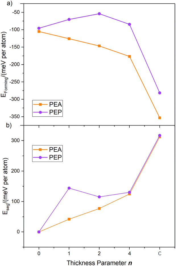 | ||
| Fig. 3 (a) Formation energy (Eform) and (b) phase segregation energy (Eseg) of PEA and PEP-based perovskites versus thickness parameter n. | ||
Note that the thermodynamic stability of PEP-based perovskites is compromised, to a certain extent, by the weaker interaction between PEP and the perovskite surface. The P–H⋯ I van der Waals interaction (H–I distance ≈ 2.70 Å) is weaker compared to the N–H⋯ I interaction in PEA-based systems (H–I distance ≈ 2.42 Å), contributing to the less negative formation energies for PEP-containing structures than their PEA-based analogs.
In terms of phase segregation energy (Fig. 3b), PEP-terminated structures exhibit consistently higher Eseg values than their PEA counterparts, indicating a greater resistance to decomposition into separated A2PbI4 and bulk (MAPbI3)n phases. This enhanced stability is attributed to the larger size and reduced polarity of the PEP cation, which allows the positively charged phosphorus center to penetrate more deeply into the [PbI6]4− framework. Structural analysis reveals that the average Pb–I bond lengths in PEP-terminated surfaces are shorter (3.13 Å in layered structures and 3.17 Å in 2D monolayers) than those in their PEA-terminated counterparts (3.19 Å and 3.35 Å, respectively), suggesting stronger electrostatic interactions between the PEP cations and the perovskite lattice. These interactions help preserve the layered gradient structure while suppressing phase segregation, particularly in thinner configurations.
3.2 Band Structure of Q2D layered perovskites PEP2PbI4·nMAPbI3versus thickness n
We computed the band structures of the Q2D perovskite series, with Fig. 4 illustrating the predicted band gaps, work functions and effective carrier masses. The calculated optical properties are listed in Table 2, while the corresponding absorbance spectra are shown in Fig. 5. Additionally, Fig. S3† presents the computed structure and properties of bulk MAPbI3 (corresponding to n = ∞). Notably, the bandgaps of the PEP2PbI4·nMAPbI3 series decrease significantly as n increases, following a similar trend observed in the PEA-based analogs, in both PBE and HSE06 calculations (see Fig. 4a). For n = 0, the rigid 2D perovskites exhibit the largest bandgaps, with PEP-based systems displaying wider bandgaps than their PEA-based analogs. The most substantial bandgap reduction occurs when n increases from 0 to 1, after which the bandgap gradually declines, approaching that of the 3D bulk MAPbI3. Additionally, we checked how the work function (Wf) varied with n (see Fig. 4b and Table S1†). A notable work function gradient is shown with the increased thickness n. This thickness-dependent bandgap and work function modulation can be leveraged to achieve “energy funneling”,17 facilitating controlled charge transport via gradient thickness variations. The projected density of states (pDOS) for PEP- and PEA-containing Q2D perovskites at various thicknesses (n), computed using PBE + SOC, are shown in Fig. S4a and S5,† while those data obtained via HSE06 + SOC are shown in Fig. S6 and S7†.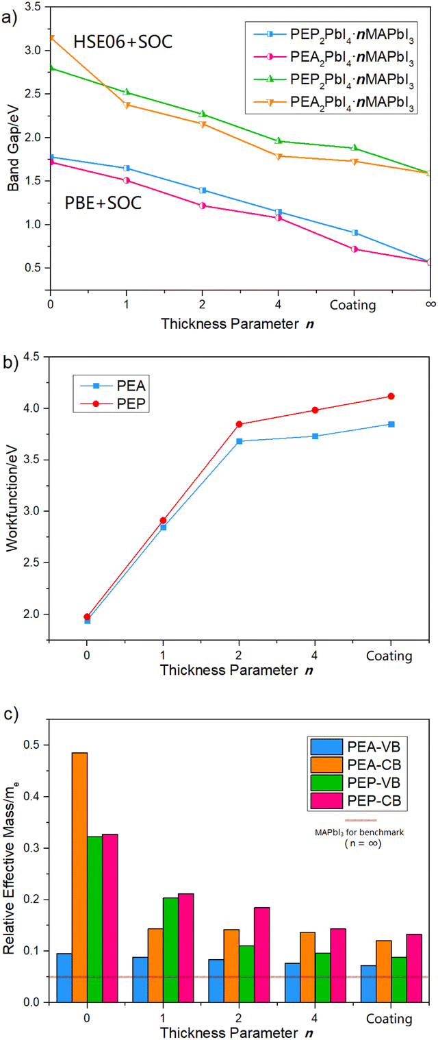 | ||
| Fig. 4 Calculated (a) bandgaps, (b) work functions and (c) effective carrier masses of PEP2PbI4·nMAPbI3 and PEA2PbI4·nMAPbI3 with various thicknesses n at the PBE + SOC level of theory. Coating refers to the structures shown in Fig. 1 | ||
| n | 0 | 1 | 2 | 4 | |
|---|---|---|---|---|---|
| OBG | PEP2PbI4·nMAPbI3 | 2.62 | 2.11 | 1.89 | 1.86 |
| PEA2PbI4·nMAPbI3 | 1.92 | 1.69 | 1.60 | 1.53 | |
| AP | PEP2PbI4·nMAPbI3 | 363 | 451 | 503 | 512 |
| PEA2PbI4·nMAPbI3 | 496 | 563 | 595 | 622 |
 | ||
| Fig. 5 Calculated absorption spectra of PEP2PbI4·nMAPbI3 and PEA2PbI4·MAPbI3 series at the HSE06 + SOC level of theory. | ||
A key characteristic of electron carriers in perovskites is their effective mass.63,64 The effective masses of carriers in the PEP2PbI4·nMAPbI3 and PEA2PbI4·nMAPbI3 series were determined by fitting the energy dispersions of the valence band maximum (VBM) and conduction band minimum (CBM) to quadratic functions, i.e.,  , where mxx and myy correspond to the effective mass components along the x and y directions, respectively. The calculated effective masses, based on the band structures (Fig. S8†), are summarized in Fig. 4c. The Q2D PEP-based perovskites, which exhibit wider bandgaps, also possess higher carrier effective masses, leading to lower carrier mobility. Consequently, Q2D multilayer PEA-based perovskites, which demonstrate higher carrier activity, may enhance the efficiency of broadband absorbers.
As displayed in Fig. 5, Q2D PEP-based perovskites with smaller thicknesses exhibit an extended absorption range in the near-ultraviolet visible region, with absorption characteristics varying as a function of thickness (n), thereby enabling tunable absorption properties. Furthermore, carrier activity gradually increases with increasing n, with the CBM carrier activity being lower in PEA-based Q2D perovskites compared to their PEP-based analogs, while the opposite trend is observed for VBM carrier activity, except at n = 0 (see Fig. S8† for calculated band structures). Based on this trend, we propose a Q2D perovskite-based tandem subcell design in the form of ETL/PEP2PbI4·n1MAPbI3/PEA2PbI4·n2MAPbI3/HTL, where n1 ≤ n2, to achieve broad absorption and high carrier mobility.
In this suggested optimized tandem configuration, the PEP-based perovskite layers are directly connected to the electron transport layer (ETL) due to their higher CBM level and carrier activity, while the PEA-based layers are interfaced with the hole transport layer (HTL) owing to their higher VBM level and carrier activity. The condition n1 ≤ n2 is essential for establishing a directional energy funnel through Q2D perovskite layer stackings of varying thicknesses, creating a band-gap gradient determined by both thickness and terminal cations. This gradient facilitates directional carrier migration, enhancing charge transport efficiency.
3.3 Carrier activities among PEP2PbI4·nMAPbI3 and PEA-based analogs with charge transfer layers
In this section, we investigate the properties of combined structures by adding CTLs on the terminals of the Q2D perovskites to simulate a more realistic subcell within tandem solar cells. Here, we chose TiO2 as the ETL and ITO (we adopt its dominant component In2O3 for calculation) as the HTL. The calculated pDOSs for the pristine CTLs are illustrated in Fig. S9,† calculated at both PBE and HSE06 + SOC levels of theory. Due to the significant lattice mismatch between the CTLs and the perovskite frameworks, we also employed larger supercells in our DFT computations. The data analysis for the latter scenario is based solely on the PBE + SOC level of theory. This heterojunction system consists of 4-layer CTLs and 3-layer perovskite frameworks, with a 20-angstrom vacuum layer introduced above the heterostructure. For the geometrical optimization, the two terminal layers adjacent to the vacuum layer were fixed, and their contributions were excluded from the electronic properties of the heterojunction system. Consequently, the minimum common multiple supercell crystal planes exhibited a lattice mismatch of less than 3%.Both three-dimensional (3D) and Q2D perovskite systems were considered in our analysis. The 3D perovskite was aligned with the HTL at the (110) orientation, while the Q2D perovskite was oriented with the A-site facing the CTLs. We computed the interface binding energies and interface distances (IDs), defined as the smallest distance from the CTL terminals to the perovskite's PbI64− frameworks (see Tables S2 and S3†). The optimized interfaces for perovskite/TiO2 are shown in Fig. S10,† and the optimized interfaces for perovskite/ITO are presented in Fig. S11.†
Our findings reveal that the surface binding energy of PEA-terminated Q2D perovskite is lower than that of PEP, regardless of whether the surface contact is with TiO2 or ITO. Although PEP cations exhibit smaller tilt angles on the perovskite surface, PEP-coated Q2D perovskites show larger IDs with the adjacent CTLs due to the greater size of PEP (dP–H = 1.42 angstroms) compared to PEA (see Table 3). This discrepancy explains why the PEA terminal demonstrates lower surface energy, influencing its response to CTL interface defects (see Section 3.4 below). With the 2D organic cation coating, the PbI64− octahedral layer of the perovskite is no longer in direct contact with the CTLs (either TiO2 or ITO) but is instead separated by the 2D PEP or PEA cations. This separation reduces the direct interaction between the mismatched lattices, leading to efficient interface passivation, as indicated by the elongated ID.
| CTL perovskite terminals | ETL (TiO2) | HTL (ITO) | ||||
|---|---|---|---|---|---|---|
| MA | PEA | PEP | MA | PEA | PEP | |
| Binding energy (meV Å−2) | −43.6 | −37.2 | −29.9 | −155.3 | −72.9 | −71.5 |
| Interface distance (Å) | 2.73 | 7.60 | 7.69 | 3.28 | 8.16 | 8.76 |
Due to the significant lattice matching ratio between the Q2D (PEP/PEA)2PbI4 series and the TiO2 electron transport layer (ETL) (see Table 4), accurately predicting the electronic structure of their heterointerface in such huge supercells exceeds the computational limits of our facility. Therefore, we focus solely on the heterointerface system involving In2O3 (ITO) (x orientation) as the HTL for electronic structure calculations.
| CTL orientation | ETL (TiO2) | HTL (ITO) | ||
|---|---|---|---|---|
| x | y | x | y | |
| 3D MAPbI3 | 2![[thin space (1/6-em)]](https://www.rsc.org/images/entities/char_2009.gif) :3 :3 |
2:5 |
1:1 |
2:3 |
| Q2D PEP(PEA)2PbI4 | 4:5 |
3:4 |
2:3 |
3:5 |
The calculated valence band BOs are +0.33 eV for the MA/ITO interface, +0.64 eV for PEA/ITO, and +0.51 eV for the PEP/ITO interface (see Fig. S12a and b†). This means that PEA cations as perovskite coatings suppress carrier non-radiative recombination better than their phosphonium derivative PEP. Meanwhile, the computed work functions (see Fig. S12c and Table S4†) show that the PEP-terminated perovskite is slightly superior to PEA homologs in terms of work function regulation due to PEP's larger size and stronger surface distortions evidenced by its smaller tilt angles. Therefore, we propose that if PEP2PbI4·nMAPbI3 was adopted as a wide-bandgap absorber, PEA2PbI4·nMAPbI3 with similar thickness n can be coated on the PEP homologs as an isomorphic layer to improve the structural stability while increasing carrier lifetimes owing to PEA's higher binding energies and larger BOs at the ITO surface.
Given that PEP-based Q2D perovskites exhibit wider bandgaps and broader absorption ranges, we suggest utilizing the narrower-bandgap PEA homologs as an intermediate transition layer. This approach offers two key benefits: improved surface stability by mitigating lattice mismatch and enhanced charge carrier transport through energy funneling. If the thickness parameter n remains identical between the two layers, the narrower-bandgap PEA domains will preferentially attract charge carriers, reducing energy loss from non-radiative recombination or phonon interactions. This design strategy for Q2D-based wide-bandgap subcells to build tandem cells can be summarized as ETL/PEP2PbI4·n1MAPbI3/PEA2PbI4·n2MAPbI3/HTL, n1 ≤ n2. A schematic carrier transfer diagram based on such a design is shown in Fig. 6, as well as the larger PEP cations tend to promote the formation of thinner Q2D structures.65
 | ||
| Fig. 6 Schematic diagrams of (a) the Q2D perovskite subcell for tandem-cell devices and (b) the predicted carrier transfer pathway through this subcell. The left brown bar refers to the VBM of HTL while the right blue bar refers to the CBM or ETL; the bandgaps of three Q2D perovskite layers in the upper panel of (a) are illustrated, correspondingly, in (b). | ||
3.4 Defect passivation within MA, PEA, and PEP perovskite terminals and ITO interface
Heterojunction defect-induced behaviors play a crucial role in carrier transition processes between the perovskite absorber and CTLs. To achieve favorable band-gap alignment with the wide band perovskite stacks, we selected a wide-bandgap MA-based perovskite, MAPbBr2Cl, rather than the narrower-bandgap MAPbI3. According to HSE06 + SOC computations, MAPbBr2Cl has a bandgap of 3.15 eV, making it a suitable benchmark for investigating the electronic properties of perovskite/HTL systems with defective HTLs. Fig. S13, S14 and Table S5† present the calculated geometric and electronic properties. To eliminate systematic errors caused by the presence of a charged vacuum layer, we excluded vacuum layers from the subsequent analysis. Since the VASP6.4 package cannot handle charged vacuum layers properly, we do not take into account charged situations in the vacuum-slab structures. In other words, all defects are considered neutral.The optimized structures used for defect formation energy and electronic structure calculations are depicted in Fig. S17,† while Fig. S16† illustrates the optimized structure of MAPbBr2Cl/ITO with defects on the ITO layer. The projected density of states (pDOS) for MAPbBr2Cl/ITO with ITO defects is shown in Fig. S17,† and a schematic representation of the trapping states is provided in Fig. 7.
 | ||
| Fig. 7 Schematic diagram of the trap states due to the defect-containing 3D MAPbBr2Cl/ITO interface structures based on Fig. S15 and S16.† “PVK” refers to “perovskite layers”. The p-type defects considered here include the antisites Ino, OIn, oxygen and indium vacancies VO and VIn, and the interstitial oxide io on the ITO layer. | ||
Based on the DFEs and IDs shown in Tables 5 and S6,† we conclude that the PEP coatings exhibit stronger suppression of defect formation than their PEA counterparts due to the higher DFEs in most types of defects. This advantage arises from PEP's larger molecular size and reduced tilt angle within the perovskite framework (see Fig. S18 and S19†). However, the pronounced p-type electronic nature of PEP coatings compromises their passivation capability.
| Defect categ. | InO | OIn | iO | VO | VIn |
|---|---|---|---|---|---|
| MAPbBr2Cl | 0.958 | 0.770 | 0.026 | 4.536 | 3.451 |
| PEA-ter. MAPbI3 | 0.319 | 1.731 | 0.531 | 0.809 | 3.401 |
| PEP-ter. MAPbI3 | −0.009 | 1.799 | 1.769 | 0.421 | 4.6013 |
In conventional 3D perovskite structures interfaced with defective ITO layers, p-type defects significantly disrupt carrier transport paths (see Fig. 7). When PEA-terminated Q2D perovskites are used, only two antisite defects—InO and OIn—generate trap states, as illustrated in Fig. 8 and supported by the pDOS calculations (Fig. S20 and S21†). In contrast, PEP-terminated Q2D perovskites exhibit three types of carrier traps: InO, OIn and VIn, suggesting a more substantial impact on charge transport, especially InO, which shows lower DFE than PEA analogs. Despite these differences, both Q2D terminal cations significantly reduce surface defect density in ITO layers by increasing defect formation energy and minimizing disruptions to the electronic structure and carrier transport pathways. Among the two, PEP coatings offer superior passivation due to their higher defect formation energy and fewer trap states during carrier transfer.
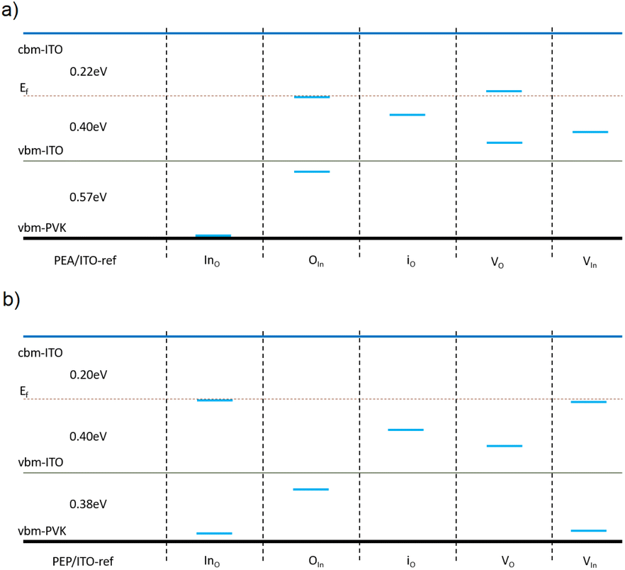 | ||
| Fig. 8 Schematic diagrams of the trap states due to the defect-containing ITO structures with the interface of Q2D (a) PEA-terminated and (b) PEP-terminated MAPbI3 perovskites. | ||
4 Conclusion
In this study, we explored a series of Q2D perovskites, PEP2PbI4·nMAPbI3, for potential application in tandem solar cells, as these Q2D perovskites likely offer tunable wide bandgaps, improved carrier transport, and enhanced defect passivation. The introduction of large PEP cations not only widens the bandgap by 0.2 eV compared to PEA-based analogs, thereby benefiting visible spectrum absorption, but also enables energy funneling through controlled thickness variation of nMAPbI3.The inclusion of Q2D organic cations at the perovskite–CTL interface prevents direct contact between the PbI64− octahedra and CTLs such as ITO. PEP cations, with their sharpened tilt angles, reduce lattice mismatch more effectively than their PEA counterparts. Conversely, PEA coatings, despite larger work-function differences, exhibit stronger carrier activity and help establish carrier migration gradients across heterostructure interfaces. As a result, PEA-based Q2D layers can serve as transitional buffers between wide bandgap PEP perovskites and CTLs.
Additionally, the Q2D cations can help to address defect-related challenges at the ITO surface, particularly near the valence band maximum. While PEP-coated films show higher formation energies for certain p-type defects, PEA-coated layers can result in improved passivation. In contrast, direct contact between 3D perovskites and defective oxide CTLs promotes low-energy defect formation, thereby hindering efficient carrier transport.
Finally, we propose that using PEP2PbI4·n1 MAPbI3 as a wide-band-gap absorber, combined with an isomorphic PEA2PbI4·n2 MAPbI3 (n1 ≤ n2) intermediate transition layer between the absorber and HTL (e.g., ITO), holds significant potential for improving tandem solar cell performance. We anticipate that future experimental validation of this design principle could lead to highly efficient tandem devices.
Data availability
The data supporting this article have been included as part of the ESI.†Author contributions
Q. L. handled the DFT computations under the supervision of X. C. Z. Both J. J. and X. C. Z. provided the funding.Conflicts of interest
The authors declare that they have no known competing financial interests or personal relationships that could have appeared to influence the research project reported in this paper.Acknowledgements
J. J. acknowledges the funding support from the National Natural Science Foundation of China (Grant No. 22303072), X. C. Z. acknowledges the support by the Hong Kong Global STEM Professorship Scheme and the Research Grants Council of Hong Kong Grant (C1055-23G and CRS Cityu 104/24).References
- A. Jena, A. Kulkarni and T. Miyasaka, Chem. Rev., 2019, 119, 3036–3103 CrossRef CAS PubMed.
- S. D. Stranks and H. J. Snaith, Nat. Nanotechnol., 2015, 10, 391–402 CrossRef CAS PubMed.
- M. Grätzel, Nat. Mater., 2014, 13, 838–842 CrossRef PubMed.
- A. Kojima, K. Teshima, Y. Shirai and T. Miyasaka, J. Am. Chem. Soc., 2009, 131, 6050–6051 CrossRef CAS PubMed.
- National Renewable Energy Laboratory, Best Research-Cell Efficiencies, 2025, available at https://www.nrel.gov/pv/cell-efficiency Search PubMed.
- Das Periodensystem der Elementeonline, 2023, available at https://web.archive.org/web/20181116050427/, http://www.periodensystem-online.de/index.php Search PubMed.
- G. Kieslich, S. Sun and A. K. Cheetham, Chem. Sci., 2015, 6, 3430–3433 RSC.
- S. Körbel, M. A. L. Marques and S. Botti, J. Mater. Chem. A, 2018, 6, 6463–6475 RSC.
- H.-Y. Zhang, Z.-X. Zhang, X.-G. Chen, X.-J. Song, Y. Zhang and R.-G. Xiong, J. Am. Chem. Soc., 2021, 143, 1664–1672 CrossRef CAS PubMed.
- H.-Y. Zhang, X.-G. Chen, Z.-X. Zhang, X.-J. Song, T. Zhang, Q. Pan, Y. Zhang and R.-G. Xiong, Adv. Mater., 2020, 32, 2005213 CrossRef CAS PubMed.
- C. M. Perez, D. Ghosh, O. Prezhdo, W. Nie, S. Tretiak and A. Neukirch, J. Phys. Chem. Lett., 2022, 13, 5213–5219 CrossRef CAS PubMed.
- S. Li, Z. Zheng, J. Ju, S. Cheng, F. Chen, Z. Xue, L. Ma and Z. Wang, Adv. Mater., 2024, 36, 2307701 CrossRef CAS PubMed.
- F. Pei, Y. Chen, Q. Wang, L. Li, Y. Ma, H. Liu, Y. Duan, T. Song, H. Xie, G. Liu, N. Yang, Y. Zhang, W. Zhou, J. Kang, X. Niu, K. L, F. Wang, M. Xiao, G. Yuan, Y. Wu, C. Zhu, X. Wang, H. Zhou, Y. Wu and Q. Chen, Nat. Commun., 2024, 15, 7024 CrossRef CAS PubMed.
- Q. Li, Y. Zheng, H. Wang, X. Liu, M. Lin, X. Sui, X. Leng, D. Liu, Z. Wei, M. Song, D. Li, H. G. Yang, S. Yang and Y. Hou, Science, 2025, 387, 1069–1077 CrossRef CAS PubMed.
- Q. Liu, M.-G. Ju and X. C. Zeng, Materials Today Energy, 2024, 42, 101556 CrossRef CAS.
- Y. Huang, T. Liu, D. Li, D. Zhao, A. Amini, C. Cheng and G. Xing, Nano Energy, 2021, 88, 106219 CrossRef CAS.
- A. M. Oddo, M. Gao, D. Weinberg, J. Jin, M. C. Folgueras, C. Song, C. Ophus, T. Mani, E. Rabani and P. Yang, Nano Lett., 2023, 23, 11469–11476 CrossRef CAS PubMed.
- L. N. Quan, M. Yuan, R. Comin, O. Voznyy, E. M. Beauregard, S. Hoogland, A. Buin, A. R. Kirmani, K. Zhao, A. Amassian, D. H. Kim and E. H. Sargent, J. Am. Chem. Soc., 2016, 138, 2649–2655 CrossRef CAS PubMed.
- M. Yuan, L. Quan and R. Comin, et al. , Nat. Nanotechnol., 2016, 11, 872–877 CrossRef CAS PubMed.
- J. Liu, J. Leng, K. Wu, J. Zhang and S. Jin, J. Am. Chem. Soc., 2017, 139, 1432–1435 CrossRef CAS PubMed.
- L. Lei, D. Seyitliyev, S. Stuard, J. Mendes, Q. Dong, X. Fu, Y.-A. Chen, S. He, X. Yi, L. Zhu, C.-H. Chang, H. Ade, K. Gundogdu and F. So, Adv. Mater., 2020, 32, 1906571 CrossRef CAS PubMed.
- N. Zhou, Y. Shen, L. Li, S. Tan, N. Liu, G. Zheng, Q. Chen and H. Zhou, J. Am. Chem. Soc., 2018, 140, 459–465 CrossRef CAS PubMed.
- K. O. Brinkmann, P. Wang, F. Lang, W. Li, X. Guo, F. Zimmermann, S. Olthof, D. Neher, Y. Hou, M. Stolterfoht, T. Wang, A. B. Djurisic and T. Riedl, Nat. Rev. Mater., 2024, 9, 202–217 CrossRef CAS.
- H. Li and W. Zhang, Chem. Rev., 2020, 120, 9835–9950 CrossRef CAS PubMed.
- J. Kromdijk, K. Glowacka, L. Leonelli, S. T. Gabilly, M. Iwai, K. K. Niyogi and S. P. Long, Science, 2016, 354, 857–861 CrossRef CAS PubMed.
- K. Bush, A. Palmstrom and Z. e. a. Yu, Nat. Energy, 2017, 2, 17009 CrossRef CAS.
- J. Werner, B. Niesen and C. Ballif, Adv. Mater. Interfaces, 2018, 5, 1700731 CrossRef.
- M. T. Horantner and H. J. Snaith, Energy Environ. Sci., 2017, 10, 1983–1993 RSC.
- F. Jiang, T. Liu, B. Luo, J. Tong, F. Qin, S. Xiong, Z. Li and Y. Zhou, J. Mater. Chem. A, 2016, 4, 1208–1213 RSC.
- J. H. Heo and S. H. Im, Adv. Mater., 2016, 28, 5121–5125 CrossRef CAS PubMed.
- D. P. McMeekin, G. Sadoughi, W. Rehman, G. E. Eperon, M. Saliba, M. T. Horantner, A. Haghighirad, N. Sakai, L. Korte, B. Rech, M. B. Johnston, L. M. Herz and H. J. Snaith, Science, 2016, 351, 151–155 CrossRef CAS PubMed.
- B. Chen, Z. Yu, A. Onno, Z. Yu, S. Chen, J. Wang, Z. C. Holman and J. Huang, Sci. Adv., 2022, 8, eadd0377 CrossRef CAS PubMed.
- Z. Song, C. Chen, C. Li, R. A. Awni, D. Zhao and Y. Yan, Semicond. Sci. Technol., 2019, 34, 093001 CrossRef CAS.
- A. Rajagopal, R. J. Stoddard, S. B. Jo, H. W. Hillhouse and A. K.-Y. Jen, Nano Lett., 2018, 18, 3985–3993 CrossRef CAS PubMed.
- S. Abdelaziz, A. Zekry, A. Shaker and M. Abouelatta, Opt. Mater., 2022, 123, 111893 CrossRef CAS.
- H. Hu, S. Moghadamzadeh, R. Azmi, Y. Li, M. Kaiser, J. C. Fischer, Q. Jin, J. Maibach, I. M. Hossain, U. W. Paetzold and B. Abdollahi Nejand, Adv. Funct. Mater., 2022, 32, 2107650 CrossRef CAS.
- C. Ding, Y. Zhang, F. Liu, Y. Kitabatake, S. Hayase, T. Toyoda, K. Yoshino, T. Minemoto, K. Katayama and Q. Shen, Nano Energy, 2018, 53, 17–26 CrossRef CAS.
- T. Minemoto and M. Murata, Sol. Energy Mater. Sol. Cells, 2015, 133, 8–14 CrossRef CAS.
- Z. Dai, S. K. Yadavalli, M. Chen, A. Abbaspourtamijani, Y. Qi and N. P. Padture, Science, 2021, 372, 618–622 CrossRef CAS PubMed.
- I. Levine, A. Al-Ashouri, A. Musiienko, H. Hempel, A. Magomedov, A. Drevilkauskaite, V. Getautis, D. Menzel, K. Hinrichs, T. Unold, S. Albrecht and T. Dittrich, Joule, 2021, 5, 2915–2933 CrossRef CAS.
- S. Y. Kim, S. J. Cho, S. E. Byeon, X. He and H. J. Yoon, Adv. Energy Mater., 2020, 10, 2002606 CrossRef CAS.
- J.-H. Kim, C.-M. Oh, I.-W. Hwang, J. Kim, C. Lee, S. Kwon, T. Ki, S. Lee, H. Kang, H. Kim and K. Lee, Adv. Mater., 2023, 35, 2302143 CrossRef CAS PubMed.
- D. S. Lee, J. S. Yun, J. Kim, A. M. Soufiani, S. Chen, Y. Cho, X. Deng, J. Seidel, S. Lim, S. Huang and A. W. Y. Ho-Baillie, ACS Energy Lett., 2018, 3, 647–654 CrossRef CAS.
- G. Jin, T. Liu, Y. Li, J. Zhou, D. Zhang, P. Pang, Z. Ye, Z. Xing, G. Xing, J. Chen and D. Ma, Nanoscale, 2022, 14, 919–929 RSC.
- W. Dong, H. Li, J. Li, Y. Hua, F. Yang, Q. Dong, X. Zhang and W. Zheng, Nano Lett., 2024, 24, 3952–3960 CrossRef CAS PubMed.
- G. Liu, X.-X. Xu, S. Xu, L. Zhang, H. Xu, L. Zhu, X. Zhang, H. Zheng and X. Pan, J. Mater. Chem. A, 2020, 8, 5900–5906 RSC.
- D. H. Kim, C. P. Muzzillo, J. Tong, A. F. Palmstrom, B. W. Larson, C. Choi, S. P. Harvey, S. Glynn, J. B. Whitaker, F. Zhang, Z. Li, H. Lu, M. F. van Hest, J. J. Berry, L. M. Mansfield, Y. Huang, Y. Yan and K. Zhu, Joule, 2019, 3, 1734–1745 CrossRef CAS.
- Y. Huang, T. Liu, D. Li, D. Zhao, A. Amini, C. Cheng and G. Xing, Nano Energy, 2021, 88, 106219 CrossRef CAS.
- G. Kresse, J. Non-Cryst. Solids, 1995, 193, 222–229 CrossRef.
- P. E. Blöchl, Phys. Rev. B: Condens. Matter Mater. Phys., 1994, 50, 17953–17979 CrossRef PubMed.
- J. P. Perdew, K. Burke and M. Ernzerhof, Phys. Rev. Lett., 1996, 77, 3865–3868 CrossRef CAS PubMed.
- S. Grimme, J. Comput. Chem., 2006, 27, 1787–1799 CrossRef CAS PubMed.
- S. Grimme, J. Antony, S. Ehrlich and H. Krieg, J. Chem. Phys., 2010, 132, 154104 CrossRef PubMed.
- J. Moellmann and S. Grimme, J. Phys. Chem. C, 2014, 118, 7615–7621 CrossRef CAS.
- J. Heyd and G. E. Scuseria, J. Chem. Phys., 2004, 120, 7274 CrossRef CAS PubMed.
- J. Heyd, G. E. Scuseria and M. Ernzerhof, J. Chem. Phys., 2003, 118, 8207 CrossRef CAS.
- A. Baldereschi, S. S. Baroni and R. Resta, Phys. Rev. Lett., 1988, 61, 1734–1737 CrossRef PubMed.
- Z. H. Wang, M. W. Zhao, X. P. Wang, Y. Xi, X. J. He, X. G. Liu and S. S. Yan, Phys. Chem. Chem. Phys., 2012, 14, 15693–15698 RSC.
- Y. C. Fan, K. Y. Hou, Z. H. Wang, T. He, X. Zhang, H. Zhang, J. Dong, X. Liu and M. W. Zhao, J. Phys. D: Appl. Phys., 2011, 44, 095405 CrossRef.
- N. R. D'Amico, G. Cantele and D. Ninno, Appl. Phys. Lett., 2012, 101, 141606 CrossRef.
- Y. Sun, L. Luan, J. Zhao, Y. Zhang, X. Wei, J. Fan, L. Ni, C. Liu, Y. Yang, J. Liu, Y. Tian and L. Duan, Mater. Sci. Semicond. Process., 2023, 168, 107822 CrossRef CAS.
- D. Meggiolaro and F. D. Angelis, ACS Energy Lett., 2018, 3, 2206–2222 CrossRef CAS.
- M. G. Ju, G. X. Sun, Y. Zhao and W. Z. Liang, Phys. Chem. Chem. Phys., 2015, 17, 17679–17687 RSC.
- J. Feng and B. Xiao, J. Phys. Chem. C, 2014, 118, 19655–19660 CrossRef CAS.
- H. Gu, J. Xia, C. Liang, Y. Chen, W. Huang and G. Xing, Nat. Rev. Mater., 2023, 8, 533–551 CrossRef CAS.
Footnote |
| † Electronic supplementary information (ESI) available. See DOI: https://doi.org/10.1039/d5ta02175h |
| This journal is © The Royal Society of Chemistry 2025 |