
 Open Access Article
 This Open Access Article is licensed under a Creative Commons Attribution-Non Commercial 3.0 Unported Licence
Unraveling the standing-up orientation transition of π-conjugated molecules on graphene templates†
Jisang
Park‡
a,
Jinhyun
Hwang‡
ab,
Byeongchan
Park
a,
Hyunji
Lee
a,
Wi Hyoung
Lee
 b,
Hyo Chan
Lee
*c and
Kilwon
Cho
*a
b,
Hyo Chan
Lee
*c and
Kilwon
Cho
*a
aDepartment of Chemical Engineering, Pohang University of Science and Technology, Pohang, 37673, South Korea. E-mail: kwcho@postech.ac.kr
bDepartment of Materials Science and Engineering, Konkuk University, Seoul 05029, South Korea
cDepartment of Chemical Engineering, Myongji University, Yongin 17058, South Korea. E-mail: hyochan@mju.ac.kr
First published on 10th March 2025
Abstract
The molecular orientation of π-conjugated organic semiconducting (OSC) thin films is critical for optimizing the performance of organic optoelectronic devices. Graphene templates have been shown to facilitate high crystallinity and large grain sizes in OSC films through π–π interactions. However, controlling the molecular orientation on graphene templates remains challenging, particularly in achieving the energetically unfavorable “standing-up” configuration of π-conjugated molecules. In this study, we systematically investigate the effects of sub-nanometer scale surface roughness and mechanical strain in graphene on the orientation of pentacene molecules in thin films. Our findings, supported by both experimental observations and density functional theory (DFT) calculations, indicate that surface roughness and strain destabilize lying-down pentacene molecules. In contrast, standing-up pentacene molecules are not affected by the changes in the physical properties of the underlying graphene templates, facilitating their transition to a standing-up orientation. This effect is further enhanced by intermolecular interactions between pentacene molecules. We believe our findings offer a novel strategy for the precise control of molecular orientation in OSC thin films.
Introduction
For decades, π-conjugated organic molecules have garnered significant attention due to their semiconducting properties when formed into thin films.1–3 Organic thin-film transistors (OTFTs), organic photovoltaics (OPVs), organic light-emitting diodes (OLEDs), and organic photodetectors based on these organic semiconducting (OSC) thin films have been successfully developed.4–7 The optoelectronic properties of OSC thin films, and consequently the performance of optoelectronic devices incorporating them, are strongly influenced by the films' crystal structures, grain sizes, and molecular orientations.8–10 Among these factors, the molecular orientation of OSC thin films is particularly critical as it dictates the anisotropy in charge transport, a key parameter in the design of optoelectronic devices.11,12 As a result, significant research efforts have been dedicated to controlling the molecular orientation of OSC thin films, along with optimizing their crystal structures and grain sizes.13,14 In recent years, the integration of OSC thin films with graphene templates has emerged as a promising avenue for advanced electronic device fabrication, offering unique opportunities for controlling film morphology and enhancing device performance. One promising approach to simultaneously control molecular orientation and optimize crystal structures and grain sizes in OSC thin films is to use graphene as a template for their growth.15,16 Graphene, a two-dimensional carbon allotrope, has a π-conjugated network,17 which facilitates π–π interactions with π-conjugated organic molecules, such as pentacene.18 These interactions promote quasi-epitaxial growth of the organic molecules on the graphene surface, enabling precise control over molecular orientation, grain growth, and overall film morphology during deposition.19 Specifically, π-conjugated organic molecules tend to adopt a lying-down molecular configuration to maximize π–π interactions with graphene, leading to OSC thin films with high crystallinity and large grain sizes.20 This approach holds particular significance for applications in flexible electronics, transparent conductors, and high-performance transistors, leveraging the unique properties of both graphene and OSC materials. Furthermore, the use of a graphene template allows for the formation of a clean atomic interface between graphene and the organic semiconductor, free from dangling bonds, improving the interface quality.21 These characteristics are especially beneficial for enhancing the performance of a range of optoelectronic devices based on organic/graphene van der Waals (vdW) heterostructures.22Despite the many advantages of using graphene as a template for OSC thin film growth, achieving molecular orientations beyond the lying-down configuration remains a significant challenge. Fabricating π-conjugated organic crystals with a standing-up molecular orientation on graphene templates is especially difficult. From a charge transport perspective, the predominance of the lying-down configuration on graphene templates strictly restricts the lateral transport of charge carriers within π-conjugated organic thin films. For this reason, organic/graphene vdW heterostructures fabricated by directly depositing organic thin films onto graphene templates are suboptimal for devices requiring efficient lateral charge transport. This highlights the need to develop methods to control molecular orientation on graphene templates.
Interestingly, a few studies have experimentally observed the formation of energetically unfavorable pentacene thin films with a standing-up molecular orientation on graphene templates under specific conditions.23,24 These conditions include contamination of the graphene surface by polymer residues, the use of graphene-coated rough Cu surfaces, and an increase in the temperature of the graphene template during pentacene deposition. However, these studies have primarily been based on empirical observations, and the underlying mechanism driving the transition from the lying-down to the standing-up configuration on graphene surfaces remains unclear. Therefore, a comprehensive investigation into this transition is crucial for developing effective strategies to control the molecular orientation of π-conjugated organic molecules on graphene templates, thus broadening the design possibilities for optoelectronic devices.
In this study, we elucidate the molecular mechanisms that govern the formation of the standing-up orientation of pentacene on graphene surfaces. We systematically investigate the effects of sub-nanometer-scale surface roughness and mechanical strain in the graphene template on the molecular orientation of pentacene thin films. Our findings, derived from both experimental observations and density functional theory (DFT) calculations, reveal that the surface roughness or strain in graphene reduces the adsorption energy of pentacene molecules in the lying-down orientation while having little to no effect on the standing-up orientation. This reduction in adsorption energy of the lying-down pentacene molecules lowers the activation energy required for the transition from the lying-down to the standing-up molecular orientation. Moreover, this effect is further enhanced by intermolecular interactions within the pentacene nuclei.
Results and discussion
Effects of graphene surface roughness on the molecular orientation of pentacene
We first investigated the molecular orientation of pentacene thin films deposited on graphene/SiO2 templates. The graphene/SiO2 templates were prepared by transferring CVD-grown graphene onto untreated SiO2/Si substrates. The templates were annealed under vacuum conditions to remove any contaminants from the graphene surface. Fig. 1a shows a typical Raman spectrum of the graphene templates. The intensity ratio of the 2D peak to the G peak was 2.1, indicating that the graphene was monolayer.25 In addition, no D peak was observed, suggesting that the defect density in the graphene was negligible. On the graphene templates, a nominal pentacene thin film with a thickness of 0.4 nm was deposited using the vapor deposition method at a deposition rate of 0.01 Å s−1 under a pressure of 10−8 Pa. This method facilitates the observation of the early growth stage.26Fig. 1b presents an AFM height image of the graphene transferred onto a flat SiO2 substrate. The surface roughness of the graphene template was measured to be approximately 0.5 nm.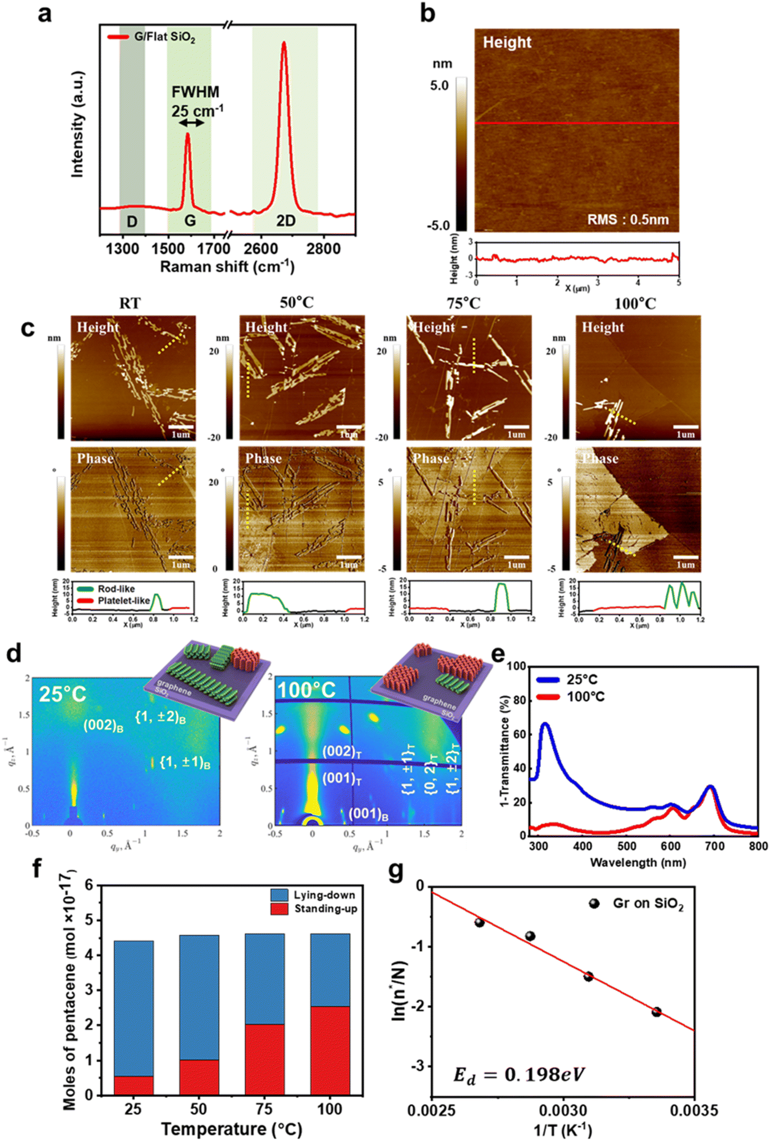 | ||
| Fig. 1 Growth evolution of pentacene thin films on graphene on flat SiO2 (G/SiO2). (a) Raman spectrum of G/SiO2. (b) AFM height image of G/SiO2. Inserted plot shows cross section view of red line on the image. (c) AFM images of pentacene thin film deposited on the G/SiO2 substrate at different temperatures. The dotted black line corresponds to the cross-sectional view shown below. In the cross-sectional view, the black line represents the graphene surface, the green line represents the rod-like island, and the red line represents the platelet-like island. (d) Two-Dimensional Grazing Incidence X-ray Diffraction (2D-GIXD) patterns of pentacene islands deposited on a flat SiO2 substrate at different temperatures (left: 100 °C, right: room temperature). (e) Ultraviolet-visible (UV-vis) spectrum of 60 nm pentacene films deposited at different temperatures (red: 100 °C, blue: room temperature). (f) Comparison of the molecular orientation in the pentacene film at different deposition temperatures, based on AFM measurements. (g) Natural logarithm of the fraction of standing-up molecules relative to the total number of molecules in the film (n*/N) as a function of the reciprocal of the substrate temperature. | ||
Fig. 1c shows the AFM images of pentacene thin films deposited on the graphene templates at various temperatures. Interestingly, both rod-like islands and platelet-like islands were observed. The rod-like islands exhibited a 10–20 nm thickness, whereas the platelet-like islands had a thickness of approximately 1.5 nm, corresponding to a single monolayer (ML) of pentacene in a standing-up orientation.27 The surface energies for the (001), (010), and (100) planes were calculated to be 3.1, 4.8, and 6.4 meV Å−2, respectively.27 When pentacene molecules adopt a lying-down orientation, the high surface energy of the (100) facet of pentacene crystals promotes growth predominantly along the (100) facets, resulting in highly elongated, rod-like pentacene islands.28 Crystals forming rod-like islands, which grow along the (100) facet, possess lower total energy due to their reduced surface energy compared to crystals exhibiting the high surface energy (001) facet. In contrast, platelet-like islands typically grow along the (001) facet and show a different growth mechanism. The higher surface energy of the (001) plane leads to a more compact and less elongated structure, promoting vertical growth of platelet-like islands.
The rod-like growth of pentacene islands indicates a lying-down orientation of pentacene molecules, while the platelet-like growth indicates a standing-up orientation.29 The lying-down orientation of pentacene molecules in rod-like islands and the standing-up orientation in platelet-like islands were confirmed by Raman spectroscopy (Fig. S1†), two-dimensional grazing incidence X-ray diffraction (GIXD) (Fig. 1d) and ultraviolet-visible spectroscopy (UV-Vis) (Fig. 1e). The GIXD pattern of a pentacene thin film deposited at 25 °C (Fig. 1d, left) exhibited intense (001) crystalline reflections along the qz direction, along with {1,±1}, {0,2}, and {1,±2} reflections aligned vertically relative to the qxy direction. These Bragg reflections confirm a highly ordered multilayered structure with molecules predominantly in a standing-up orientation.30 In contrast, the (001) reflection along the qxy direction was weak, indicating a lower presence of lying-down molecules. However, when the pentacene thin film was deposited at 100 °C, the GIXD pattern changed significantly. The (001) reflections appeared at an 18° tilt relative to the qxy direction but were indistinct along the qz direction (Fig. 1d, right). These reflection spots correspond to the lying-down molecular arrangement in bulk or single-crystal pentacene.23 UV-Vis spectroscopy further supported this structural difference. The film deposited at 25 °C exhibited a strong absorption peak near 330 nm (3.7 eV), which was less pronounced in the film grown at 100 °C (Fig. 1e). This peak corresponds to the S0–S3 transition, whose dipole moment has B2u symmetry.31 Since this transition is enhanced by a lying-down molecular arrangement, its prominence in the film deposited at 25 °C confirms the dominance of lying-down pentacene molecules in this film.
Based on the shape of pentacene islands observed in the AFM images, we calculated the number of pentacene molecules with lying-down and standing-up orientations as a function of deposition temperature. The surface area and height of the rod-like and platelet-like islands were extracted from the AFM data and used to model the 3D volume of each island type. The total volume of the rod-like and platelet-like islands was then multiplied by the number density of pentacene single crystals (2.84 molecules per nm3) to determine the total number of pentacene molecules in each type of island. The results are shown in Fig. 1f. Interestingly, as the deposition temperature increased, the total number of deposited pentacene molecules remained nearly constant. However, the fraction of standing-up pentacene molecules increased from 12.4% to 55.0% with the increasing deposition temperature from 25 °C to 100 °C.
The lying-down configuration is predicted to be energetically favorable for individual pentacene molecules due to strong π–π interactions between the graphene and pentacene molecules. This observation is consistent with our findings of predominantly lying-down pentacene islands at low deposition temperatures. However, the difference in adsorption energy between a lying-down pentacene molecule and a standing-up pentacene molecule was 1.68 eV on a graphene surface, as discussed in detail later. Therefore, the formation of standing-up pentacene thin films on graphene at high deposition temperatures cannot be explained if the system is considered simply as a single pentacene molecule on perfectly flat graphene. The formation of standing-up pentacene islands on graphene suggests that additional factors significantly reduce the energy difference between lying-down and standing-up pentacene molecules inside islands formed on graphene (Ed). We estimated this energy difference, Ed, from the ratio of the number of standing-up molecules (n*) to the total number of molecules (N) (n*/N) as a function of deposition temperature, using a Boltzmann factor.32
| n*/N ∝ exp(−Ed/KBT) |
As a result, Ed was estimated to be 0.198 eV on the graphene/SiO2 substrate (Fig. 1g).
To investigate the factors influencing the molecular orientation of pentacene thin films, we conducted the same experiments as shown in Fig. 1 but with differently prepared graphene templates. Before transferring the graphene, a SiO2/Si substrate was immersed in a low concentration of n-octadecyl trichlorosilane (ODTS) in a humidity-controlled glove box to form an ODTS self-assembled monolayer (SAM) on the SiO2 surface. The graphene was transferred onto this SAM layer via wet transfer, creating a graphene/ODTS/SiO2 template (G/ODTS/SiO2).
The insertion of a well-ordered ODTS SAM between the graphene and SiO2 surfaces is known to reduce the roughness of the graphene surface.33 Additionally, it decreases the amplitude of electron–hole puddles in graphene by increasing the distance between the graphene and charged impurities on the SiO2 substrate. The reduction of the amplitude of electron–hole puddles is confirmed by Raman spectroscopy,34 which shows that the full width at half maximum (FWHM) of the G peak for G/ODTS/SiO2 is 15 cm−1, smaller than that for G/SiO2, which is 25 cm−1 (Fig. 2a). AFM imaging confirmed that the surface roughness of the graphene decreased to approximately 0.25 nm after SAM treatment, compared to the roughness of 0.50 nm for the untreated graphene/SiO2 template (Fig. 2b and c).
 | ||
| Fig. 2 Growth evolution of pentacene thin films on graphene on SAM coated SiO2 (G/SAM). (a) Raman spectrum of G/SAM. (b) AFM height image of G/SAM. (c) Histogram of the normalized frequency of roughness on different substrates (red: graphene/SiO2, gray: graphene/ODTS) (d) AFM images of pentacene thin film deposited on G/SAM substrate at different temperatures. (e) Comparison of the molecular orientation in the pentacene film at different deposition temperatures, based on AFM measurements. (f) Natural logarithm of the fraction of standing-up molecules relative to the total number of molecules in the film (n*/N) as a function of the reciprocal of the substrate temperature. | ||
Fig. 2d shows AFM images of pentacene islands on G/ODTS/SiO2 templates deposited at various temperatures. Like the graphene/SiO2 templates, the deposition temperature had little effect on the total number of pentacene molecules deposited on the graphene/ODTS/SiO2 templates (Fig. 2e). However, compared to G/SiO2 templates, the fraction of standing-up molecules (n*/N) at a deposition temperature of 25 °C noticeably decreased to 0.046. On the other hand, the fraction n*/N approached 0.58 when the deposition temperature was 100 °C, comparable to that of G/SiO2 at the same deposition temperature. The dependence on the deposition temperature reveals that Ed for the G/ODTS/SiO2 templates is 0.351 eV (Fig. 2f), which is higher than the Ed of 0.198 eV on the graphene/SiO2 substrate.
In summary, the results presented in Fig. 1 and 2 indicate that the presence of surface roughness, electron–hole puddles on the graphene surface, or both can significantly reduce the energy difference, Ed, between lying-down and standing-up pentacene molecules within islands formed on graphene templates. This reduction in Ed facilitates the observed transition from a lying-down to a standing-up orientation of pentacene molecules, a phenomenon that will be addressed in more detail later. At this stage, further research is needed to isolate the effects of surface roughness and electron–hole puddles.
Effects of graphene strain on the molecular orientation of pentacene
In addition to investigating the roughness of graphene surfaces, we examined the effects of strain in graphene on the molecular orientation of pentacene thin films. Mechanically deformed graphene was prepared through the following procedure: First, silica nanospheres (NSs) with a diameter of 200 nm were spin-coated onto a SiO2/Si substrate, resulting in closely packed clusters of nanospheres. Subsequently, graphene was wet-transferred onto the silica nanospheres (G/NS). Finally, the sample was annealed at 400 °C in a vacuum to remove undesired polymer residues from the graphene surface.35,36Fig. 3a presents a typical AFM image of an annealed G/NS sample. The topography reveals two distinct regions: one where graphene was suspended between nanospheres and another where graphene was directly in contact with the underlying nanospheres. Notably, wrinkles in the graphene connecting adjacent nanospheres were observed, indicating the presence of radial tensile strain in the graphene.36 Raman spectroscopy further confirmed the tensile strain in the graphene (Fig. 3b). Compared to graphene transferred onto a flat substrate, both the G peak and the 2D peak were red-shifted. The ratio of the 2D peak shift to the G peak shift was approximately 2.2, suggesting that the shifts were predominantly due to tensile strain rather than changes in doping levels.37
 | ||
| Fig. 3 Effects of tensile strain and surface roughness in graphene on the orientation of pentacene thin films. (a) AFM image of annealed graphene on G/NS template. (b) Raman spectra of G/NS template compared to flat graphene. (c) AFM image showing the formation of two-dimensional platelet-like pentacene islands on the G/NS template. (d) Raman spectrum of pentacene thin films deposited on the G/NS template. | ||
We deposited pentacene thin films with a nominal thickness of 0.4 nm onto the annealed G/NS template. Interestingly, this led to the predominant formation of two-dimensional platelet-like pentacene islands (Fig. 3c), suggesting a standing-up orientation of the pentacene molecules. This orientation was further confirmed by Raman spectroscopy. The Ag band at 1533 cm−1 and the B3g band at 1596 cm−1 are characteristic Raman peaks for pentacene thin films.38 Previous studies have shown that the B3g band exhibits zero Raman intensity when the long axis of the pentacene molecules is perpendicular to the laser's electric field used in Raman measurements.38 Therefore, when the pentacene molecules adopt a standing-up configuration, the Ag band is prominent, while the B3g band is not. Consequently, the intensity ratio of the B3g band to the Ag band (I1596/I1533) can determine the molecular orientation of pentacene on graphene substrates: a negligible I1596/I1533 ratio indicates a standing-up configuration. Fig. 3d shows the Raman spectrum of pentacene thin films deposited on the annealed G/NS template. The Ag band at 1533 cm−1 is observed, while the B3g band at 1596 cm−1 is much less prominent. The resulting I1596/I1533 ratio was 0.30, suggesting a predominantly standing-up orientation of the pentacene molecules.
For comparison, we also deposited pentacene thin films with a nominal thickness of 0.4 nm on non-annealed G/NS templates. In the absence of the annealing process after transferring graphene onto nanospheres, no significant tensile strain was applied to the graphene, as confirmed by Kelvin probe force microscopy (KPFM) analysis (Fig. S3a†) and Raman spectroscopy analysis (Fig. S3b†). On the non-annealed G/NS template, rod-like pentacene islands were formed, in contrast to the annealed G/NS templates (Fig. S4a†). Additionally, the I1596/I1533 ratio from the Raman spectrum of the pentacene islands was 6.15 (Fig. S4b†), which suggests that the islands predominantly contain lying-down pentacene molecules.
It is important to note that in a previous study using graphene templates transferred onto flat substrates,23 pentacene islands with a standing-up orientation were formed on non-annealed graphene, while lying-down pentacene islands were observed on clean, annealed graphene. This difference was attributed to polymer residues on the surface of non-annealed graphene, which hindered π–π interactions between the graphene and pentacene molecules. However, the formation of standing-up pentacene islands on the annealed G/NS array, where PMMA residues were eliminated, and lying-down pentacene islands on the non-annealed G/NS array contradicts previous observations. Here, the only significant differences between the non-annealed and annealed G/NS arrays were the presence of PMMA residues and the strain level in the graphene. Because the presence of PMMA residues alone cannot account for our observations, we conclude that the sizable tensile strain in the annealed G/NS array induced the formation of standing-up pentacene thin films.
DFT studies on the molecular orientation of pentacene on graphene templates
To gain insights into the mechanisms governing the observed formation of standing-up pentacene islands on rough or strained graphene, we performed density functional theory (DFT) calculations (see the Experimental section for details). Fig. 4 presents the molecular configurations of pentacene on graphene surfaces with varying degrees of surface roughness and strain. We specifically modeled the pentacene molecules in three distinct orientations: lying-down (0°), tilted (45°), and standing-up (90°). Additionally, we considered three types of graphene surfaces: a flat surface, a slightly convex-curved surface with a radius of curvature of 2 Å, and a significantly convex-curved surface with a radius of curvature of 4 Å. The adsorption energy per molecule (Eads) was calculated using the equation:| Eads = (Egraphene+pentacene − Egraphene − nEpentacene)/n |
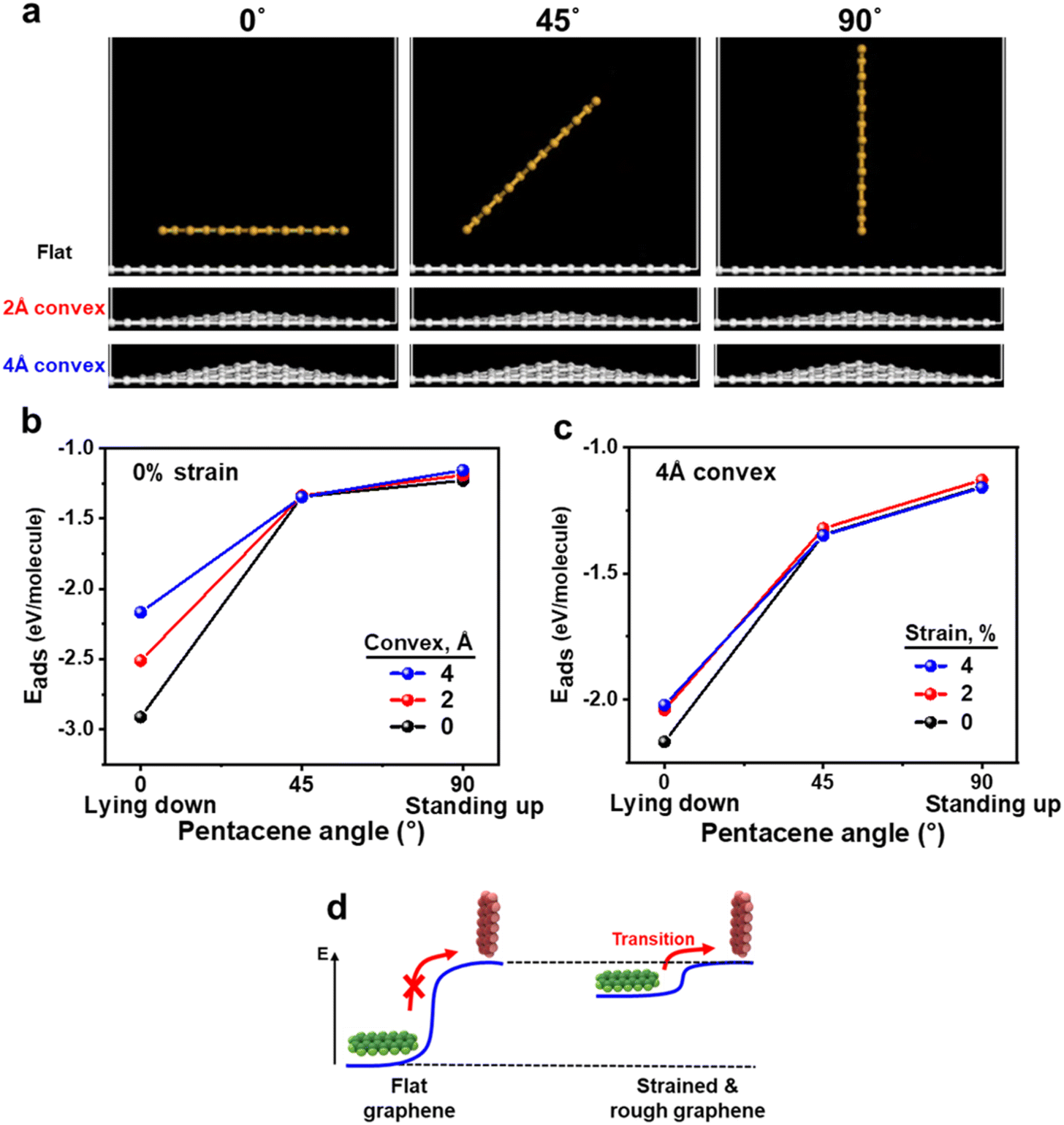 | ||
| Fig. 4 DFT analysis of pentacene adsorption on graphene with varying surface roughness and strain. (a) Molecular configurations of pentacene on graphene surfaces, modeled in three orientations: lying-down (0°), tilted (45°), and standing-up (90°), across flat, slightly convex (2 Å curvature), and significantly convex (4 Å curvature) graphene surfaces. (b) Adsorption energy Eads of a single pentacene molecule as a function of its molecular orientation (0°, 45°, and 90°) on unstrained graphene surfaces with varying curvatures. (c) Adsorption energy of pentacene molecules on a graphene surface with a 4 Å curvature as a function of strain (0% to 4%). (d) Overview of the DFT calculations showing the impact of graphene lattice modifications on the adsorption energy of pentacene molecules. | ||
Fig. 4b shows the adsorption energy of a single pentacene molecule (n = 1) as a function of its molecular orientation (0°, 45°, and 90°) on unstrained graphene surfaces with varying curvatures. The adsorption energy decreases monotonically in all cases as the orientation shifts from 0° to 90°. This suggests that the difference in adsorption energy between the standing-up orientation (Eads(90°)) and lying-down orientation (Eads(0°)),
| ΔEads = Eads(90°) − Eads(0°) |
| Strain (%) | Adsorption energy (Eads) | ||||
|---|---|---|---|---|---|
| E ads(0°) (lying-down) | E ads(45°) | E ads(90°) (standing-up) | E ads(90°) − Eads(0°) | ||
| Flat | 0 | −2.913 | −1.343 | −1.228 | 1.685 |
| 2 | −2.806 | −1.308 | −1.202 | 1.604 | |
| 4 | −2.764 | −1.314 | −1.2300 | 1.5350 | |
| 2Å convex | 0 | −2.511 | −1.337 | −1.189 | 1.321 |
| 2 | −2.372 | −1.312 | −1.1622 | 1.210 | |
| 4 | −2.357 | −1.338 | −1.1950 | 1.162 | |
| 4Å convex | 0 | −2.167 | −1.346 | −1.155 | 1.012 |
| 2 | −2.040 | −1.321 | −1.129 | 0.911 | |
| 4 | −2.021 | −1.349 | −1.1590 | 0.862 | |
Fig. 4d provides an overview of the DFT results, illustrating the impact of graphene lattice modifications, such as surface roughness and strain, on the adsorption energy of pentacene molecules. Our findings indicate that these modifications do not significantly alter the stability of the standing-up pentacene orientation. In the standing-up configuration, the pentacene molecules have minimal interaction with the graphene surface due to their vertical alignment, which prevents additional π–π interactions and limits the contact area. Consequently, modifications to the graphene lattice, such as strain or surface roughness, have little influence on the adsorption energy of this configuration. In contrast, the lying-down orientation, which relies on strong π–π interactions with the graphene surface, is notably destabilized by increased surface roughness or strain. This destabilization significantly reduces the energy barrier for pentacene molecules to transition from a lying-down to a standing-up orientation, thereby promoting the formation of standing-up pentacene islands.
The adsorption energy of a single pentacene molecule on graphene surfaces qualitatively explains our observations. However, the ΔEads values estimated from DFT calculations deviate significantly from the experimentally observed Ed (0.198 eV) for graphene/SiO2 templates (Fig. 1). We believe this discrepancy is primarily due to the nature of intermolecular interactions between pentacene molecules, which were not fully captured in the single-molecule models shown in Fig. 4b and c. We calculated Eads for n pentacene molecules adsorbed on a flat, unstrained graphene surface to support this hypothesis.
Fig. 5a shows the adsorption configurations of n pentacene molecules on the graphene surface used for the calculation. This DFT calculation assumes that the coverage of pentacene molecules on graphene is in the sub-monolayer regime, with no aggregation of pentacene molecules in the vertical direction, as we aim to simulate a scenario before the nucleation of pentacene islands. For the lying-down orientation, n pentacene molecules are modeled to form AB-stacking with the underlying graphene. For the standing-up orientation, n pentacene molecules are modeled to aggregate to maximize the contact area between pentacene molecules. In this case, Eads is influenced by both pentacene–pentacene interactions and pentacene–graphene interactions, unlike the single-molecule scenario. Fig. 5b shows Eads for lying-down and standing-up pentacene molecules when n pentacene molecules are adsorbed on the graphene surface (n = 1, 2, 3, 4). For the lying-down orientation, Eads for the scenario of two pentacene molecules decreases slightly by 0.304 eV mol−1 per pentacene molecule compared to the Eads for a single pentacene molecule. This weak intermolecular interaction is expected, as no π–π interaction but the steric hindrances between the hydrogen atoms occur between the pentacene molecules in this configuration. Conversely, for the standing-up orientation, the Eads decreases by 0.349 eV mol−1 with the addition of a second pentacene molecule. Unlike the lying-down orientation, this reduction in Eads indicates that the intermolecular interactions within the pentacene crystal on graphene are attractive, likely due to strong π–π interactions between the standing-up pentacene molecules. Consequently, on a flat, unstrained graphene surface, the adsorption energy difference between the standing-up and lying-down configuration, ΔEads of 1.685 eV mol−1 for the single pentacene model is significantly reduced to 1.032 eV mol−1 for the two-pentacene model. As the number of pentacene molecules, n, increases, this trend becomes more prominent. When four pentacene molecules are considered, ΔEads is further reduced to 0.520 eV mol−1. This reduction in ΔEads with increasing n clearly illustrates that the accumulation of pentacene molecules before nucleation on the graphene surface facilitates the transition from the lying-down to a standing-up orientation.
 | ||
| Fig. 5 (a) Adsorption configurations of aggregated pentacene molecules on graphene. (b) Adsorption energy of n pentacene molecules on flat, unstrained graphene, considering pre-nucleus aggregation. | ||
To summarize, based on the DFT results shown in Fig. 4 and 5, we propose that pentacene islands with a standing-up molecular orientation can be achieved on graphene templates under the following conditions: First, the lattice of graphene should be modified to weaken the π–π interactions between graphene and lying-down pentacene molecules. Second, the surface concentration of pentacene molecules on graphene must be sufficiently high before the nucleation of pentacene islands.
Experimental
Fabrication of silica nanosphere arrays
Silica nanospheres with a diameter of 200 nm, dispersed in deionized water at a concentration of 10 mg mL−1 (purchased from nanoComposix, SISN200-25M), were utilized. The SiO2/Si substrates, featuring a 300 nm thick SiO2 layer, were cleaned sequentially with isopropanol, acetone, and subjected to ultraviolet ozone (UVO) treatment. To optimize the size and enhance the degree of close-packing of the nanosphere arrays, the spin-coating process was executed in three stages, with rotational speeds set at 200, 500, and 1500 rpm for durations of 30, 30, and 60 seconds, respectively.39Synthesis and transfer of graphene
Graphene was synthesized on copper foil via chemical vapor deposition (CVD) following previously established methods.40 A poly(methyl methacrylate) (PMMA) layer dissolved in chlorobenzene was spin-coated at 3000 rpm for 60 seconds, followed by baking at 120 °C for 30 minutes to remove residual solvents. To eliminate graphene on the reverse side of the copper foil, oxygen plasma treatment was performed using a reactive ion etcher. The copper foil was then etched using a 0.05 M ammonium persulfate solution, followed by rinsing through floating on deionized water for one hour. The silica nanosphere array on the 300 nm SiO2/Si wafer underwent UVO treatment for 30 minutes prior to the transfer of graphene. The graphene was carefully transferred onto the nanosphere array and dried under moderate vacuum conditions to prevent rupture. Post-transfer, the graphene was immersed in acetone for 3 hours to dissolve the PMMA, followed by hydrogen annealing at 400 °C for 2 hours to remove any residual PMMA.Pentacene deposition
Pentacene was deposited using the same methodology as previously employed.33 Organic molecular beam deposition (OMBD) was used to deposit pentacene thin films (Aldrich Chemicals, 99.99% purity) in ultra-high vacuum (UHV, 10−8 Torr). The substrate temperature was kept at room temperature, and the deposition rate was 0.1 Å s−1.Fabrication of self-assembled monolayer (SAM) substrate
We utilized octadecyltrichlorosilane (ODTS) to transfer graphene onto substrates with SAM layers. To form an ordered SAM, SiO2 substrates were immersed in a SAM solution within a glove box where temperature, humidity, and pressure were meticulously controlled in the freezer. After immersion, the substrates underwent a 2 minute rinsing with toluene, followed by 2 minutes of sonication to remove loosely adhering SAM clusters. To strengthen the interaction between the SAM layer and the substrate, the samples were baked at 120 °C for 20 minutes. Additional cycles of sonication and rinsing was followed, after which the graphene was transferred onto the substrates via a wet transfer method.DFT calculations
The DFT calculations were conducted using the generalized gradient approximation (GGA) with the Perdew–Burke–Ernzerhof (PBE) exchange-correlation functional, implemented in the CASTEP module of Materials Studio 2020. To accurately model the van der Waals interactions, which play a key role in the adsorption processes, a dispersion correction was applied to the PBE functional following the Tkatchenko and Scheffler (DFT-TS) approach. Ultrasoft pseudopotentials were used to represent core electrons, while valence electrons were treated explicitly. The geometries of both graphene and pentacene were optimized independently using a vacuum slab of 20 Å thickness to prevent spurious interactions between periodic images. The optimization process continued until energy convergence was achieved within 1 × 10⁻⁵ eV per atom, with force and displacement thresholds set at 0.03 eV Å−1 and 0.001 Å, respectively. The plane-wave basis set had an energy cutoff of 450 eV, and a 1 × 1 × 1 k-point grid was employed for the slab calculations.Conclusions
In conclusion, we have elucidated the mechanisms that determine the molecular orientation of pentacene on graphene templates. Our experimental findings demonstrate that sub-nanometer scale surface roughness or tensile strain in graphene promotes the formation of pentacene islands with a standing-up configuration. DFT calculations support these observations. The calculations reveal that the adsorption energy of standing-up pentacene molecules is minimally affected by the surface roughness or strain of the underlying graphene surface. In contrast, the surface roughness or strain weakens the adsorption of lying-down pentacene molecules, thereby significantly reducing the activation energy required for the transition from a lying-down to a standing-up orientation. This activation energy is further reduced when intermolecular interactions between pentacene molecules are considered, as the intermolecular interactions between standing-up pentacene molecules are much stronger than those between lying-down pentacene molecules. This work provides new insights into the molecular orientation control of π-conjugated organic molecules on graphene templates. Our findings offer a foundation for developing methods to control the molecular orientation of organic thin films precisely. Such advancements could potentially enhance the design and performance of next-generation optoelectronic devices based on OSC/graphene heterostructures.Data availability
The data supporting this article have been included as part of the ESI.†Conflicts of interest
There are no conflicts to declare.Acknowledgements
This work was supported by the National Research Foundation of Korea (NRF) grant (2020R1A2C3004477, 2022R1C1C1013173) funded by the Ministry of Science and ICT (MSIT), Korea.Notes and references
- A. Facchetti, Chem. Mater., 2011, 23, 733–758 CrossRef CAS.
- C. Wang, H. Dong, W. Hu, Y. Liu and D. Zhu, Chem. Rev., 2012, 112, 2208–2267 Search PubMed.
- L. Zang, Y. Che and J. S. Moore, Acc. Chem. Res., 2008, 41, 1596–1608 CrossRef CAS PubMed.
- B. Geffroy, P. le Roy and C. Prat, Polym. Int., 2006, 55, 572–582 Search PubMed.
- X. Guo, Y. Xu, S. Ogier, T. N. Ng, M. Caironi, A. Perinot, L. Li, J. Zhao, W. Tang, R. A. Sporea, A. Nejim, J. Carrabina, P. Cain and F. Yan, IEEE Trans. Electron Devices, 2017, 64, 1906–1921 Search PubMed.
- J. Shin, M. Kim, B. Kang, J. Lee, H. G. Kim and K. Cho, J. Mater. Chem. A, 2017, 5, 16702–16711 Search PubMed.
- C. Wang, H. Dong, L. Jiang and W. Hu, Chem. Soc. Rev., 2018, 47, 422–500 Search PubMed.
- R. R. Lunt, J. B. Benziger and S. R. Forrest, Adv. Mater., 2010, 22, 1233–1236 Search PubMed.
- A. Troisi and G. Orlandi, J. Phys. Chem. A, 2006, 110, 4065–4070 CrossRef CAS.
- A. A. Virkar, S. Mannsfeld, Z. Bao and N. Stingelin, Adv. Mater., 2010, 22, 3857–3875 Search PubMed.
- V. Coropceanu, J. Cornil, D. A. da Silva Filho, Y. Olivier, R. Silbey and J.-L. Brédas, Chem. Rev., 2007, 107, 926–952 CrossRef CAS PubMed.
- Z. Shuai, H. Geng, W. Xu, Y. Liao and J.-M. André, Chem. Soc. Rev., 2014, 43, 2662–2679 RSC.
- X. Bai, K. Zong, J. Ly, J. S. Mehta, M. Hand, K. Molnar, S. Lee, B. Kahr, J. M. Mativetsky, A. Briseno and S. S. Lee, Chem. Mater., 2017, 29, 7571–7578 CrossRef CAS.
- Y. Watanabe, D. Yokoyama, T. Koganezawa, H. Katagiri, T. Ito, S. Ohisa, T. Chiba, H. Sasabe and J. Kido, Adv. Mater., 2019, 31, 1808300 CrossRef.
- S. B. Jo, H. H. Kim, H. Lee, B. Kang, S. Lee, M. Sim, M. Kim, W. H. Lee and K. Cho, ACS Nano, 2015, 9, 8206–8219 CrossRef CAS.
- N. N. Nguyen, H. Lee, H. C. Lee and K. Cho, Acc. Chem. Res., 2022, 55, 673–684 CrossRef CAS.
- J. Chen, Y. Xu, Y. Liu, H. Liu, H. Zhang, L. Jin, L. Shi, Y. Lan, Y. Zou and J. Fan, Adv. Funct. Mater., 2024, 34, 2313027 CrossRef CAS.
- M. Chhikara, G. Bratina and E. Pavlica, ACS Omega, 2023, 8, 27534–27542 CrossRef CAS.
- H. Huang, S. Chen, X. Gao, W. Chen and A. T. S. Wee, ACS Nano, 2009, 3, 3431–3436 CrossRef CAS PubMed.
- N. N. Nguyen, H. C. Lee, B. Kang, M. Jo and K. Cho, Nano Lett., 2019, 19, 1758–1766 CrossRef CAS PubMed.
- H. Yang, J. Heo, S. Park, H. J. Song, D. H. Seo, K.-E. Byun, P. Kim, I. Yoo, H.-J. Chung and K. Kim, Science, 2012, 336, 1140–1143 CrossRef CAS PubMed.
- M. Gobbi, E. Orgiu and P. Samorì, Adv. Mater., 2018, 30, 1706103 CrossRef PubMed.
- W. H. Lee, J. Park, S. H. Sim, S. Lim, K. S. Kim, B. H. Hong and K. Cho, J. Am. Chem. Soc., 2011, 133, 4447–4454 CrossRef CAS PubMed.
- S. Wen, Y. Liu, J. Shen, P. Zhao, X. Cai, Y. Luo, X. Li, Y.-H. Lu, F. Song and W.-D. Dou, Appl. Surf. Sci., 2023, 613, 156156 CrossRef CAS.
- L. M. Malard, M. A. Pimenta, G. Dresselhaus and M. S. Dresselhaus, Phys. Rep., 2009, 473, 51–87 CrossRef CAS.
- J. Hwang, J. Park, J. Choi, T. Lee, H. C. Lee and K. Cho, Adv. Sci., 2024, 11, 2400598 CrossRef CAS.
- J. E. Park, M. Son, M. Hong, G. Lee and H. C. Choi, Angew. Chem., Int. Ed., 2012, 51, 6383–6388 CrossRef CAS PubMed.
- J. E. Northrup, M. L. Tiago and S. G. Louie, Phys. Rev. B: Condens. Matter Mater. Phys., 2002, 66, 121404 CrossRef.
- M. Hodas, P. Siffalovic, P. Nádaždy, N. a. Mrkyvková, M. Bodík, Y. Halahovets, G. Duva, B. Reisz, O. Konovalov, W. Ohm, M. Jergel, E. Majková, A. Gerlach, A. Hinderhofer and F. Schreiber, Appl. Nano Mater., 2018, 1, 2819–2826 CrossRef CAS.
- D. H. Kim, H. S. Lee, H. Yang, L. Yang and K. Cho, Adv. Funct. Mater., 2008, 18, 1363–1370 CrossRef CAS.
- F. Anger, J. O. Ossó, U. Heinemeyer, K. Broch, R. Scholz, A. Gerlach and F. Schreiber, J. Chem. Phys., 2012, 136, 054701 CrossRef CAS.
- S. Nagai, Y. Inaba, T. Nishi and S. Tomiya, Appl. Phys. Express, 2022, 15, 015502 CrossRef CAS.
- N. N. Nguyen, H. C. Lee, K. Baek, M. S. Yoo, H. Lee, H. Lim, S. Choi, C.-J. Kim, S. Nam and K. Cho, Adv. Funct. Mater., 2021, 31, 2008813 CrossRef CAS.
- Q. H. Wang, Z. Jin, K. K. Kim, A. J. Hilmer, G. L. C. Paulus, C.-J. Shih, M.-H. Ham, J. D. Sanchez-Yamagishi, K. Watanabe, T. Taniguchi, J. Kong, P. Jarillo-Herrero and M. S. Strano, Nat. Chem., 2012, 4, 724–732 CrossRef CAS PubMed.
- M. Yamamoto, O. Pierre-Louis, J. Huang, M. S. Fuhrer, T. L. Einstein and W. G. Cullen, Phys. Rev. X, 2012, 2, 041018 CAS.
- Y. Zhang, M. Heiranian, B. Janicek, Z. Budrikis, S. Zapperi, P. Y. Huang, H. T. Johnson, N. R. Aluru, J. W. Lyding and N. Mason, Nano Lett., 2018, 18, 2098–2104 CrossRef CAS PubMed.
- J. E. Lee, G. Ahn, J. Shim, Y. S. Lee and S. Ryu, Nat. Commun., 2012, 3, 1024 CrossRef.
- L. Zhang, S. S. Roy, R. J. Hamers, M. S. Arnold and T. L. Andrew, J. Phys. Chem. C, 2015, 119, 45–54 CrossRef CAS.
- S. S. Shinde, S. Park and J. Shin, J. Semicond., 2015, 36, 043002 CrossRef.
- N. N. Nguyen, S. B. Jo, S. K. Lee, D. H. Sin, B. Kang, H. H. Kim, H. Lee and K. Cho, Nano Lett., 2015, 15, 2474–2484 CrossRef CAS PubMed.
Footnotes |
| † Electronic supplementary information (ESI) available. See DOI: https://doi.org/10.1039/d5ta00895f |
| ‡ Jisang Park and Jinhyun Hwang contributed equally to this work. |
| This journal is © The Royal Society of Chemistry 2025 |