
 Open Access Article
 This Open Access Article is licensed under a Creative Commons Attribution-Non Commercial 3.0 Unported Licence
Engineering stable p-type contacts towards efficient fully vacuum deposited perovskite solar cells†
Arghanoon
Moeini
 ,
Kassio P. S.
Zanoni
,
Cristina
Roldán-Carmona
* and
Henk J.
Bolink
*
,
Kassio P. S.
Zanoni
,
Cristina
Roldán-Carmona
* and
Henk J.
Bolink
*
Instituto de Ciencia Molecular (ICMol), Universidad de Valencia, C/Catedrático J. Beltrán 2, 46980 Paterna, Spain. E-mail: Cristina.Roldan@uv.es; Henk.Bolink@uv.es
First published on 24th March 2025
Abstract
Perovskite photovoltaics have recently achieved significant breakthroughs in cell efficiency, while offering simple and low-cost processability. Vacuum-based techniques are gaining increased attention due to their scalability and material versatility. However, fully vacuum-deposited devices remain rare, partly due to the limited availability of charge transport materials compatible with vacuum deposition. Additionally, sublimed organic contact materials often require high work function interlayers, such as MoO3, or molecular oxidants, which complicate device stability. In this study we explore the use of simpler non-extended conjugated self-assembled monolayers (SAMs) as alternatives to these high work function interlayers, demonstrating improved hole extraction, higher fill factors, and enhanced long-term stability compared to state-of-the art vacuum-deposited architectures. As a proof of concept, devices incorporating SAMs/TaTm (N4,N4,N4′′,N4′′-tetra([1,1′-biphenyl]-4-yl)-[1,1′:4′,1′′-terphenyl]-4,4′′-diamine) interfaces and methylammonium lead iodide perovskite (MAPbI3) achieve power conversion efficiencies exceeding 19.5%, approaching the highest reported values for fully evaporated stacks, along with remarkable thermal stability at 85 °C.
1 Introduction
Metal-halide perovskites have rapidly emerged as a leading material class for photovoltaic and optoelectronic applications due to their excellent optoelectronic properties, structural flexibility, and low-cost manufacturing,1–5 enabling high power conversion efficiency (PCE) with strong integrability. To date, the record efficiency of perovskite solar cells (PSCs) has exceeded 25%6 but the device's long-term stability and the development of scalable and reliable fabrication methods are pending challenges for their commercialization. Most of the investigations reported in the literature have focused on solution-based fabrication methods, either using small- or large-scale techniques like spin-coating, slot-die coating or inkjet printing.7–13 However, many of these methods may be less pertinent for their transfer to market as they employ toxic solvents that are detrimental to the environment.14 Physical vacuum deposition is a mature solvent-free technology already established in the semiconductor industry,15 which has recently gained increasing attention in the perovskite field. Among different advantages, vacuum deposition provides superior control over the layer thickness, intrinsic purity of the sublimed materials, and it allows the preparation of multilayer stacks with conformal coating over different types of substrates. This is of special interest to broaden the market towards alternative applications like building integrated PVs, Internet of things (IoT) or multi-junction tandem solar cells.16–18 Since 2016, efficient devices (>20% PCE) using vacuum-deposited (VD) perovskites have been successfully demonstrated in both p-type/intrinsic/n-type (n–i–p) and p–i–n configurations, combining either organic polymers, small-molecular-weight semiconductors,19 or inorganic metal oxides (i.e. SnO2, TiO2 or NiOx) as charge selective layers.20–22 Nevertheless, despite the promise of vacuum deposition, finding stable charge-selective layers to fully realize evaporated devices, particularly for hole transport (HTL), remains a challenge.23–25In search for the ideal HTL, one should ensure high hole mobility, high thermal and chemical stability, and adequate electronic level alignment to provide ohmic charge transfer to the electrode. In addition, the substrate plays a crucial role in the growth of VD perovskites and may promote detrimental chemical reactions taking place at the interface. This happens when inorganic metal oxides such as CuOx,26 NiOx,27 or MoOx,28 are used. In these metal oxides the acid–base reactions result in local degradation of the perovskite and the formation of an electrical barrier for hole harvesting.24,29–31 As an alternative, sublimable “small molecule” semiconductors such as arylamine or polythiophene derivatives are good candidates,20,21,32,33 but their intrinsic nature provides a non-ohmic interface with ITO, thus hindering charge injection/collection. Only when these small molecular conjugated materials are used as very thin layers (<3 nm) have good device performances been obtained. However, this is highly prone to coating defects. Alternatively, co-deposition or the addition of an interlayer of an oxidizing material can also improve the formation of ohmic contacts.34–36 The latter usually consists of strong electron-acceptor dopants,32 such as cyano-quinodimethane derivatives (F4-TCNQ and F6-TCNNQ) or metal oxides such as MoO3 (ref. 37 and 38) or W2O3,39 which induce free positive charges at the interface with the organic semiconductor, enabling ohmic charge transport.39,40 A typical example is the hole selective interface MoO3/TaTm, with TaTm being an intrinsic semiconductor successfully utilized in multiple high-efficiency devices. Unfortunately, these interlayers are unstable at elevated temperatures,40 thus compromising device stability. Indeed, little information can be obtained regarding the lifetime of efficient (>18%) fully vacuum deposited PSCs using these interlayers, with the exception of a few reports, the majority of which show very short stability tests with timescales ranging from seconds to ∼200 h.15,41–45
For future high-throughput commercialization, it is crucial to ensure stable high ϕ interfaces with minimal parasitic absorption, ideally based on low-cost materials suitable for a variety of substrates and areas. A recent trend in perovskite PV is the use of phosphonic acids containing carbazole molecules that can self-assemble on metal oxide surfaces (SAMs) as HTMs. These materials have demonstrated minimal recombination losses and improved device stability, in part due to the critical chemical design that leads to reduced interfacial recombination.45–48 However, simpler SAMs which lack the extended π-conjugation and electron delocalization also present an opportunity for creating stable, dopant-free interlayers that can be paired with sublimable intrinsic semiconductors, expanding the potential of fully evaporated devices. Despite few studies using simpler SAMs as electrode modifiers,49,50 or for interface defect passivation for metal oxides, their use as interlayers in perovskite PVs remains largely unexplored.
Here, we investigate non-extended conjugated phosphonic acid SAMs to evaluate their properties as high ϕ interlayers at the well-stablished ITO/TaTm interface, comparing them with benchmark interlayers such as MoO3 or F6-TCNNQ. We explore a series of phosphonate systems featuring increasing amounts of fluorine-terminated groups, in both alkyl and simple aromatic structures, designed to introduce a permanent dipole moment at the interface and modulate the work function (ϕ) of ITO. These modified ITOs are then integrated into p–i–n fully vapor-deposited perovskite solar cells (VD-PSCs), and their performance and stability are compared to those of state-of-the-art devices. Remarkably, devices using the archetypal methylammonium lead iodide perovskite (MAPbI3) and SAM interlayers achieve an impressive average power conversion efficiency (PCE) of ∼19.5%, closely matching record efficiencies reported for fully evaporated stacks. The results reveal a strong correlation between device efficiency and the induced high ϕ, leading to improved hole extraction, higher fill factor (FF), and overall enhanced performance. Even more significant is the stability advantage: the absence of unstable oxides or dopants results in superior thermal stability under prolonged stress at 85 °C, bringing the performance closer to the durability observed in solution-processed analogues. Notably, this approach holds great potential for broader applications, offering the flexibility to adapt to various device architectures and perovskite formulations, with promising potential for compatibility with conformal coverage on large-area and textured substrates—a key factor for scaling up to industrial production.
2 Results and discussion
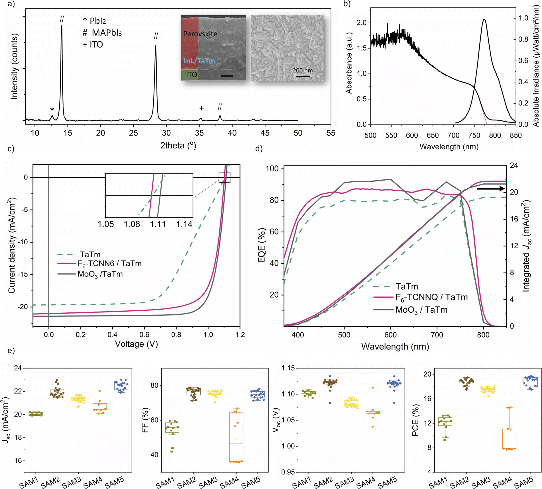
Fig. 1a shows the chemical structures of the SAM molecules and TaTm, along with the device architecture used in this study. We selected commercially available SAMs with phosphonic acid as the anchoring group to ensure a strong, reproducible interaction with the ITO surface, as this group can form multiple stable bonds.51 The SAMs investigated include phenylphosphonic acid (SAM 1), 4-fluorobenzylphosphonic acid (SAM 2), ((3-trifluoromethyl)phenyl)methyl-phosphonic acid (SAM 3), decylphosphonic acid (SAM 4), and 1H,1H,2H,2H-perfluorooctanephosphonic (SAM 5). These molecules feature increasing levels of fluorine-terminated groups, contributing to variations in dipole moment, film coverage and packing. Specifically, SAM 1 and SAM 4 contain a non-substituted phenyl group and an aliphatic, non-conjugated structure, offering neutral reference points that allow for a comparison of surface energy effects. They are widely used, inexpensive, and thermally stable, making them practical choices for large-scale applications. SAM 2, SAM 3 and SAM 5 incorporate fluorinated moieties, which are strongly electron-withdrawing and expected to increase the ITO work function while also enhancing hydrophobicity. After modifying the ITO electrodes with SAMs, they were transferred directly to the vacuum deposition system without any additional processing (further details can be found in the Experimental section). Fig. S1† illustrates the changes in wettability of the ITO surface, measured by using the water contact angle (θ). Increased hydrophobicity at the ITO surface is noteworthy because ITO is a polar hydrophilic oxide, which is often chemically incompatible with non-polar organic thin films.52 Therefore the enhanced surface hydrophobicity improves direct electrical contact with organic semiconductors such as TaTm, reducing the risk of delamination of the upper organic layer. The value of θ for bare-ITO (UV–ozone treated) increases significantly after surface treatment, from ∼0° to 43° for SAM 1, due to the presence of the hydrocarbon tail group. The introduction of fluorine enhances this effect, with θ reaching 50.7° for SAM 2 (1 fluorine) and 71.2° for SAM 3 (3 fluorine moieties). The most dramatic increase occurs for the aliphatic SAMs – 90° for SAM 4 and 97° for SAM 5 – indicating strong hydrophobicity at these new interfaces. Additionally, Fig. S1† presents the 3D scan images and root mean square (RMS) roughness data for the same contacts, measured by atomic force microscopy (AFM). The RMS roughness of the bare-ITO surface remains relatively unchanged after SAM deposition (3.6 nm to 4.7 nm), indicating a uniform and flat surface without significant island formation. Yet, there is a complete transformation in the energy landscape of the interfaces. Fig. 1b shows a schematic of the energy level alignment diagrams of ITO/TaTm contacts. The bare ITO surface has a large energy gap (∼0.6 eV) between its Fermi level (EF ∼ 4.8 eV)53,54 and the highest occupied molecular orbital (HOMO) of TaTm (∼5.4 eV).53 Typically, this gap is bridged using thin interlayers included as references in the left panel of Fig. 1b such as MoO3 or dopants like F6-TCNNQ.54,55 | ||
| Fig. 1 (a) Chemical structures of SAMs, TaTm and device architecture of p–i–n VD-PSCs. (b) Schematic showing the energy level diagram of the p-type ITO/TaTm contact containing typical MoO3 or F6-TCNNQ high ϕ materials (left) and a SAM interlayer (right). (c) ϕ of the SAM-modified ITO interfaces measured by the KP technique. The values for bare ITO and the HOMO of TaTm are indicated with inset lines as the reference. The values of μz, taken from the literature,56–59 are also included with the exception of SAM 4. | ||
Instead, here we use SAM 1–5 to modulate the interface properties via surface dipoles, aiming to closely match these energy levels (right panel, Fig. 1b). Because the modulation of the interface depends strongly on the SAM dipole orientation, as well as molecular packing and density, we measured the shift in ϕ for each sample using the Kelvin probe technique (KP) (Fig. 1c). The dashed lines represent the ϕ value for bare-ITO, and the HOMO level of TaTm, shown here as references. For comparison, the molecular dipole projection onto the surface normal axis (μz) for those SAMs that are available in the literature is also included.56,60 Consistent with previous studies, we observe an increase in the ϕ that aligns with the trend of μz, for the new interfaces. In the case of aryl-derivatives, a gradual increase in ϕ is observed when adding fluorine units, from 0.14 eV (SAM 1) to a maximum change in ϕ of 0.73 eV (SAM 3). For the aliphatic derivatives, the increase is more moderate, from 0.19 eV (SAM 4) to 0.4 eV (SAM 5). Such an increase in ϕ indicates the formation of a surface dipole pointing outward (i.e. with its positive pole facing ITO), which can hence provide better control of the energy band alignment with the HTM, and promote the formation of an ohmic contact.
To gain insights into the chemical bonding and structural modifications at the ITO–SAM surface, we conducted X-ray photoelectron spectroscopy (XPS) analysis. The spectra were measured using a monochromatized Al K-alpha with a photon energy of 1486.6 eV, allowing for highly surface sensitive measurements. Fig. 2 presents the relevant XPS core level regions, showing the P 2p, O 1s, and In 3d signals from the ITO–SAM interfaces. In the P 2p region, the primary component of the P–O bond (∼132.8 eV) appears as a doublet, corresponding to the spin–orbit splitting of the P 2p level, with an expected separation of 0.9 eV.61 Compared to the powder samples (Fig. S2†), we observe a general change in the peak intensities and shift to lower binding energy. These shifts suggest modifications in the chemical environment of the phosphorus atoms, consistent with the formation of metal–phosphonate bonds with ITO.
 | ||
| Fig. 2 (a) High resolution P 2p, O 1s, and In 3d XPS spectra of SAMs 1–5 deposited on ITO (1 × 1) cm2. The intensity of the In 3d signals for SAMs 1–3 has been multiplied by a factor of 103. (b) Schematic sketch of the bonding configurations of phosphonic acids to oxide surfaces. The label shows each type of oxygen chemical environment in a different color, with the theoretical intensity ratio of the O 1s components in brackets. | ||
Similarly, the O 1s signal (530–532 eV) shows changes in both the peak position and relative peak intensities, due to variations in P![[double bond, length as m-dash]](https://www.rsc.org/images/entities/char_e001.gif) O and P–OH bonds after surface functionalization. Fig. 2b presents a schematic of possible bonding configurations for phosphonic acids to ITO. Each oxygen atom's chemical environment corresponds to a distinct binding energy, meaning that various bonding configurations will display multiple O 1s components with different intensity ratios (see the theoretical ratios of the O 1s components in brackets, arranged from high- to low-binding energy). According to the schematic, when the molecule is in the powder state (left side of Fig. 2b), the O 1s spectrum mainly consists of two peaks corresponding to P–OH (∼533.5 eV, orange) and PO (∼532.5 eV, blue) groups, with a 2
O and P–OH bonds after surface functionalization. Fig. 2b presents a schematic of possible bonding configurations for phosphonic acids to ITO. Each oxygen atom's chemical environment corresponds to a distinct binding energy, meaning that various bonding configurations will display multiple O 1s components with different intensity ratios (see the theoretical ratios of the O 1s components in brackets, arranged from high- to low-binding energy). According to the schematic, when the molecule is in the powder state (left side of Fig. 2b), the O 1s spectrum mainly consists of two peaks corresponding to P–OH (∼533.5 eV, orange) and PO (∼532.5 eV, blue) groups, with a 2![[thin space (1/6-em)]](https://www.rsc.org/images/entities/char_2009.gif) :1 intensity ratio. Occasionally, a minor peak (∼534 eV) is observed, generally associated with adsorbed species such as water or oxygen (see Fig. S2† for powder XPS O 1s spectra). However, after SAM deposition, two new peaks emerge corresponding to the substrate oxygen atoms (∼530.5 eV, green) and the covalent P–O–M bonds (∼531.5 eV, pink), providing different intensity profiles for each monodentate, bidentate, or tridentate configuration. The O 1s peaks in Fig. 2a are color-coded for clarity. For the aryl-based SAMs (SAM 1, SAM 2 and SAM 3), the signal deconvolutes into three components, with the main peak at ∼532.5 eV (PO), and minor peaks at ∼533.5 eV (P–OH) and ∼531.5 eV (P–O–M). The prevalence of PO alongside P–OH and P–O–M could indicate the formation of weakly bounded monodentate configurations.62–64 However, the absence of a substrate oxygen signal (∼530 eV) and the intensity profile of O 1s for SAMs 1–3 suggest the accumulation of non-binding molecules possibly forming multilayer structures. This is further supported by the minimal In 3d signal (444–445 eV), which is characteristic of the ITO substrate. Such significant reduction indicates that the atoms of In at the surface are no longer exposed to the XPS probing depth, consistent with thick molecular layer coverage. In contrast, the O 1s signals of aliphatic SAMs (SAM 4 and SAM 5) are dominated by the substrate oxide peak (∼530 eV), and the P–O–M bond (∼531.6 eV), with a small shoulder at ∼532.5–533.07 eV. As depicted in Fig. 2b, the dominance of the P–O–M signal (pink) suggests strong bonding configurations, like tridentate or bidentate deprotonated bonds. In this case, the O 1s intensity ratios for SAM 4 and 5 (0:1:3 and 1:0:5 respectively) align with the formation of a monolayer featuring mixed tridentate and bidentate deprotonated configurations. This is corroborated by the much higher In 3d signal, comparable to that of the bare ITO substrate.
:1 intensity ratio. Occasionally, a minor peak (∼534 eV) is observed, generally associated with adsorbed species such as water or oxygen (see Fig. S2† for powder XPS O 1s spectra). However, after SAM deposition, two new peaks emerge corresponding to the substrate oxygen atoms (∼530.5 eV, green) and the covalent P–O–M bonds (∼531.5 eV, pink), providing different intensity profiles for each monodentate, bidentate, or tridentate configuration. The O 1s peaks in Fig. 2a are color-coded for clarity. For the aryl-based SAMs (SAM 1, SAM 2 and SAM 3), the signal deconvolutes into three components, with the main peak at ∼532.5 eV (PO), and minor peaks at ∼533.5 eV (P–OH) and ∼531.5 eV (P–O–M). The prevalence of PO alongside P–OH and P–O–M could indicate the formation of weakly bounded monodentate configurations.62–64 However, the absence of a substrate oxygen signal (∼530 eV) and the intensity profile of O 1s for SAMs 1–3 suggest the accumulation of non-binding molecules possibly forming multilayer structures. This is further supported by the minimal In 3d signal (444–445 eV), which is characteristic of the ITO substrate. Such significant reduction indicates that the atoms of In at the surface are no longer exposed to the XPS probing depth, consistent with thick molecular layer coverage. In contrast, the O 1s signals of aliphatic SAMs (SAM 4 and SAM 5) are dominated by the substrate oxide peak (∼530 eV), and the P–O–M bond (∼531.6 eV), with a small shoulder at ∼532.5–533.07 eV. As depicted in Fig. 2b, the dominance of the P–O–M signal (pink) suggests strong bonding configurations, like tridentate or bidentate deprotonated bonds. In this case, the O 1s intensity ratios for SAM 4 and 5 (0:1:3 and 1:0:5 respectively) align with the formation of a monolayer featuring mixed tridentate and bidentate deprotonated configurations. This is corroborated by the much higher In 3d signal, comparable to that of the bare ITO substrate.
Finally, the F 1s signal changes notably after surface functionalization (Fig. S2†), shifting from a single peak (∼688 eV) to multiple deconvoluted peaks. In the 688–686.5 eV range, these peaks suggest distinct chemical environments, likely due to van der Waals interactions within the fluorinated structure, which indicates less homogeneous molecular packing compared to the powder. However, the peak at ∼684.5 eV likely corresponds to the formation of metal–fluorine bonds with ITO62 and is particularly significant for SAM 2 and SAM 3, where multilayers are observed. Table 1 summarizes the peak positions and their relative contributions to the O 1s signal for each SAM interlayer.
| P–OH | PO |
M–OH/P–O–M | Metal oxide (bulk) | |
|---|---|---|---|---|
| SAM 1 | 533.5 (17%) | 532.6 (68%) | 531.3 (15%) | — |
| SAM 2 | 533.6 (10%) | 532.6 (75%) | 531.1 (15%) | — |
| SAM 3 | 533.3 (26%) | 532.3 (62%) | — | 530.7 (12%) |
| SAM 4 | — | 532.7 (13%) | 531.6 (35%) | 530.3 (52%) |
| SAM 5 | 533.1 (6%) | — | 531.6 (29%) | 530.3 (65%) |
| ITO | 531.0 (9%) | 529.8 (91%) |
We additionally evaluated the ITO–SAM/TaTm hole extraction interfaces by fabricating fully VD-PSCs. The device architecture includes modified ITO–SAM, followed by a previously reported architecture containing TaTm (7 nm)/MAPbI3 (800 nm)/C60 (25 nm)/BCP (8 nm)/Ag (100 nm) in which C60 is fullerene and BCP is bathocuproine, as shown in Fig. 1a. To ensure reliable statistics, we fabricated more than 30 cells for each device configuration, and over 40 cells in the case of the best performing devices. Fig. 3a shows the X-ray diffraction (XRD) pattern of the as-deposited MAPbI3 film, along with top and cross-sectional scanning electron microscopy (SEM) images. The films consist of a polycrystalline material with small grains (<200 nm in diameter), typical of vacuum co-deposited PSCs, and a minor presence of a residual PbI2 phase.63 The UV-vis absorption and photoluminescence (PL) spectra, shown in Fig. 3b, confirm the high absorption coefficient and a bandgap of ∼1.6 eV, which are typical for MAPbI3. We characterized a series of devices by measuring the current density vs. voltage (J–V) curves under AM 1.5 G sun illumination, from which the relevant PV performance parameters were extracted. Initially, we analysed devices containing the intrinsic semiconductor, TaTm, alongside those incorporating state-of-the-art interlayers like MoO3 and F6-TCNNQ. The representative J–V curves, and external quantum efficiency (EQE) of reference devices are summarized in Fig. 3c and d, with the specific PV values listed in Table S1.† A statistical comparison of the photovoltaic parameters is shown in Fig. S3,† and the champion cells for each underlayer are shown in Fig. S4 and Table S2.† Regardless of the cell configuration, similar average Jsc (∼20.6 mA cm−2), and Voc (∼1.1 V) are observed, but notable differences appear in the average FF. Devices with only a 7 nm TaTm layer exhibit low FF values (∼55.5 ± 1.4%), and a reduced slope near the Voc (Fig. 3c), indicating significant series resistance. This is expected due to the low conductivity of TaTm and the large energy mismatch with ITO, resulting in an average power conversion efficiency PCE of 12.3 ± 1.7%. While reducing the TaTm thickness to 3 nm leads to an improvement in the FF (70 ± 1.2%) (Fig. S3†),34 such thin layers are prone to inhomogeneities, leading to inconsistent device performance. By contrast, the introduction of MoO3 and F6-TCNNQ interlayers significantly enhances device efficiency. While Voc (∼1.10 V) and Jsc (>20 mA cm−2) show only slight improvement, the FF increases markedly to ∼80%, resulting in average PCE values exceeding 19%. The increased Jsc is consistent with the higher current integrated from EQE (Fig. 3d). This behaviour, well documented in the literature, is attributed to interfacial positive charges induced by high ϕ interlayers, promoting ohmic contact behaviour and boosting device performance. However, these interfaces are prone to deactivation, which results in unstable solar cells, and makes the strategy less appealing for the market. Interestingly, we achieve comparable efficiency by introducing ITO–SAM (1–5)/TaTm interfaces. The photovoltaic performance, as shown in Fig. 3e, strongly depends on the SAM chemical structure, and is particularly promising for the fluorinated SAMs. For the non-fluorinated interlayers, SAM 1 and SAM 4, the Jsc is slightly below 21 mA cm−2 and the FF remains low, barely surpassing 60%. These values are well below those of the MoO3 or F6-TCNNQ interlayers, and are similar to those of pristine TaTm devices. For the aryl derivative SAM 1, the Voc remains at ∼1.1 ± 0.004 V, while in the case of the aliphatic SAM 4, it slightly drops to 1.05 ± 0.009 V, resulting in a PCE of ∼12% for both. This aligns with the lower ϕ values observed for SAM 1 and SAM 4 (Fig. 1c), reflecting hindered charge extraction at the interface. In contrast, using fluorinated derivatives, SAM 2, SAM 3 and SAM 5, significantly improves the FF to around 80% (76 ± 2; 75 ± 1; 74 ± 2% respectively), with PV parameters closely matching those of the reference devices. Notably, SAM 2 and SAM 5 deliver high Voc (∼1.13 V) and Jsc (∼22 mA cm−2), outperforming the reference cells. This results in an average efficiency of ∼19% (18.7 ± 0.5; 18.8 ± 0.7 respectively), with negligible J–V hysteresis. Even in the case of SAM 3, where alignment with the TaTm HOMO level may not be optimal, the device still exhibits improved Jsc and FF compared to the 7–3 nm TaTm-only devices, reaching an average PCE of 17.5 ± 0.4%.
 | ||
| Fig. 3 (a) XRD patterns and (b) optical absorption and PL spectra of co-sublimed perovskite films. (c) J–V and (d) EQE curves obtained for the reference VD p–i–n PSCs, under AM 1.5 G (100 mW cm−2) illumination. The integrated Jsc was obtained by integrating the EQE spectrum obtained with the AM 1.5 G photon flux spectrum. The EQE measurement was performed on unencapsulated devices in an inert atmosphere with the corresponding setup mentioned in Section 4.4. (e) Statistical analysis of photovoltaic parameters obtained for cells containing SAM-modified ITO interfaces using the optimal TaTm thickness (5 nm for aromatic SAMs and 7 nm for aliphatic SAMs). The top bar shows the maximum value, the bottom bar shows the minimum value, and the rectangle shows the region containing 25–75% of the data, obtained for each condition. The total device area is 0.0825 cm2, with an illuminated area of 0.05 cm2. The cells, measured in air, are encapsulated with 30 nm of Al2O3. | ||
A summary of the device optimization for SAM 2, SAM 3 and SAM 5, with varying TaTm thicknesses from 5 to 13 nm, can be found in the ESI (Fig. S5–S7).† In all three cases, the device performance is significantly impacted by TaTm thickness, with thicker layers (10–13 nm) leading to a significant drop in efficiency due to increased resistance from the intrinsic semiconductor. As the TaTm thickness is reduced, the behaviour differs depending on the SAM interlayer. For the aryl-derivatives, SAMs 2 and 3, a consistent improvement in the photovoltaic parameters Jsc, Voc and FF is observed, with optimal performance achieved at a TaTm thickness of 5 nm. SAM 5 follows a similar trend, but it experiences a noticeable drop in efficiency when the TaTm layer is reduced below 7 nm, driven by a decline in all key photovoltaic parameters. This behaviour may be linked to the thinner nature of SAM 5, as suggested by the XPS analysis, making it more susceptible to coverage defects and enhanced charge recombination at thinner TaTm layers. As a result, while the optimal TaTm thickness for SAMs 2 and 3 is 5 nm, SAM 5 performs best with a thickness ranging between 5 and 10 nm. The best performing cells for each configuration, including the J–V curves and EQE, are summarized in Fig. 4, and listed in Table S3.† High photon-to-current conversion efficiencies of over 80% are observed across most of the ultraviolet-visible spectrum, resulting in integrated current densities of 20.7, 21.13 and 21.6 mA cm−2 for SAM 3, SAM 2 and SAM 5 respectively, in line with the J–V curves. Notably, the monolayer SAM 5 outperforms the others, with Jsc, Voc and FF values of 22.6 mA cm−2; 1.12 V; 77.3% respectively, leading to an overall efficiency of 19.65% (see J–V hysteresis measurements in Fig. S8†). These results suggest that similar device performances to those of state-of-the-art fully VD-PSCs can be achieved by omitting critical interlayers such as MoO3 or F6-TCNNQ, and instead using simpler SAM interlayers, provided the interface induces a sufficient change in the ITO ϕ.
 | ||
| Fig. 4 (a) J–V and (b) EQE curves of the champion cells using SAM 2, 3, and 5 measured under AM 1.5 G illumination (100 mW cm−2). The EQE measurement was performed on encapsulated devices with the corresponding setup mentioned in Section 4.4. (c) Device stability under continuous thermal stress at 85 °C, measured in a N2 atmosphere. The cells contain the optimal TaTm thickness (5 nm for SAM 2 and SAM 3, and 7 nm for SAM 5). The total device area is 0.0825 cm2, with an illuminated area of 0.05 cm2. The cells, measured in air, are encapsulated with 30 nm of Al2O3. | ||
The stability of the devices was also evaluated under high temperature conditions. Fig. 4c shows the stability curves for unsealed solar cells using SAM 2, 3 and 5, measured under continuous thermal stress (500 h) at 85 °C in a nitrogen atmosphere. For comparison, the stability of devices with MoO3 or F6-TCNNQ under the same conditions is provided in Fig. S9.† A significant improvement in device stability is observed when substituting MoO3 or F6-TCNNQ with SAM 2, SAM 3 or SAM 5. As shown in Fig. S9,† the MoO3 or F6-TCNNQ interlayers degrade rapidly, losing over 20% of their initial efficiency within just 100 h. After this point, their performance sharply declines, with efficiency dropping below 50% once the test reaches 500 h. A closer examination of the device parameters reveals that Voc (and to a lesser extent Jsc) did not degrade significantly, particularly for the MoO3 interlayer. Instead, the FF, mainly responsible for the drop in performance, reduces to 75% of its initial value after just 100 hours of the test. In contrast, the SAM interlayers exhibit no significant signs of FF degradation, and both Voc, and Jsc only show a gradual but minor decrease. As a result, cells with SAM interlayers retain over 78% of their initial efficiency after 500 h, with SAM 2 and 5 maintaining 85% and 92% efficiency respectively. Therefore, not only are the charges more efficiently extracted to the external contacts, but they also result in enhanced thermal stability for the devices. Importantly, SAM 5 demonstrates remarkable long-term stability, retaining 90% of its initial efficiency after 1000 hours of testing (Fig. S10†). These findings indicate that the degradation dynamics of the interface might be influenced by the type of molecule and its molecular packing. Controlling these interactions may widen the exploration of SAMs, providing a new plethora of novel p-type contacts in fully evaporated devices.
3 Conclusions
In summary, we evaluated several simple-structure SAMs as novel high ϕ interlayers to use as p-type contacts in combination with intrinsic sublimable semiconductors. By incorporating modified ITO–SAM electrodes to overcome the energy barrier at the TaTm interface, we observed improvements in both efficiency and stability of fully VD-PSCs, primarily due to the preservation of FF stability over time. Our findings indicate that aryl-derivative SAMs tend to form multilayers, unlike their aliphatic analogues, leading to small differences in the optimal TaTm thickness. Overall, the primary factor influencing device performance and stability is the work function modulation, which improves the ohmic contact at the ITO/HTM interface, and facilitates more efficient charge extraction for the fluorinated SAMs. Additionally, by preserving these properties under thermal stress, charge accumulation and interfacial recombination are reduced over time, ultimately enhancing the operational stability of the device, unlike the reference interlayers. Exploiting this simple concept allows the fabrication of fully evaporated MAPbI3 solar cells with PCE exceeding 19%, while also enhancing thermal stability. These results highlight the versatility of SAMs as stable, efficient interlayers for fully VD-PSCs, and open the door to further exploration of p-/n-type contacts in the quest for even higher efficiencies and greater stabilities.4 Experimental section
4.1. Materials
Photolithographically patterned ITO-coated glass substrates were purchased from Naranjo Substrates. N4,N4,N4′,N4′-tetra([1,1′-biphenyl]-4-yl)-[1,1′:4′,1′-terphenyl]-4,4′-diamine (TaTm) was provided by TCI America. Phenylphosphonic acid (SAM 1), 4-fluorobenzylphosphonic acid (SAM 2), ((3-trifluoromethyl)phenyl)methyl-phosphonic acid (SAM 3), decylphosphonic acid (SAM 4), 1H,1H,2H,2H-perfluorooctanephosphonic (SAM 5), fullerene (C60) and PbI2 were purchased from Sigma-Aldrich. CH3NH3I (MAI), MoO3, bathocuproine (BCP), and 1,3,4,5,7,8-hexafluorotetracyanonaphthoquinodimethane (F6-TCNNQ) were purchased from Luminescence Technology Corp.4.2. Cell fabrication
The patterned ITO glass substrates were cleaned with soap, deionized water, and isopropanol in an ultrasonic bath, followed by a UV–O3 treatment for 20 minutes. The last step of substrate preparation consisted of immersing the ITO substrates in 1 mmol per l concentration of phosphonic acid solution (SAMs 1–5) prepared in ethanol overnight. After this step, the substrates were annealed at 100 °C for 10 minutes and washed with pure ethanol to remove the excess molecules. The modified ITO substrates were directly transferred to the sublimation vacuum chambers, integrated into an inert nitrogen atmosphere (pressure of 10−6 mbar, H2O and O2 < 0.1 ppm). TaTm, C60 and BCP were sublimed in the same vacuum chamber at temperatures ranging from 130 °C to >300 °C, depending on the material, following the same deposition recipe with a rate of 0.2 Å s−1. The perovskite films were fabricated by co-subliming the PbI2 and MAI precursors from separate crucibles. Each material was heated to its respective sublimation point using Creaphys crucibles, and the deposition rates were measured using two separate Quartz Crystal Microbalance (QCM) sensors. One sensor was positioned at the height of the substrate holder for close, precise monitoring of the rate, while the other one was placed close to the PbI2 source to facilitate the rate maintenance throughout the process; however, the first sensor was the reference for the ratio calculations. To achieve a MAPI film with a slight PbI2 excess, PbI2 was evaporated at a rate of 0.50 Å s−1 as measured by a substrate sensor. Subsequently, MAI was added, which led to an increase in the substrate sensor reading to 0.65 Å s−1. During the evaporation of the organic precursor, a temporary increase in the chamber pressure was observed due to the degassing of the material, which then stabilized.59 The total perovskite thickness used in this work has been measured to be 720 nm. The silver electrodes were deposited in a separate vacuum chamber using tungsten boat sources, at rates ranging from 1.0 to 2.5 Å s−1. Finally, a thin layer of Al2O3 was deposited via atomic layer deposition as an encapsulant on photolithographically patterned ITO-coated glass substrates.4.3. Film characterization
The surface topography of the thin film was analysed using an Atomic Force Microscopy (AFM) measurement, which was performed with a Bruker Multimode AFM equipped with a Nano Scope V. This was done in tapping mode using silicon tips with a natural resonance frequency of 300 kHz and an equivalent constant force of 40 N m−1. The resulting data were then processed using Gwyddion scanning probe microscopy data analysis software. Scanning electron microscopy (SEM) images were obtained on a Hitachi S-4800 microscope operated at an accelerating voltage of 1 kV. X-ray diffraction was measured using a surface diffractometer Empyrean from Panalytical equipped with a Cu Kα anode. The UV-vis absorption measurements were performed using a tungsten–halogen lamp, connected to a spectrometer. Steady-state photoluminescence measurements were conducted using an excitation laser with a wavelength of 520 nm. Both PL and absorbance measurements were conducted using an Avantes Avaspec-2048L optical detector (Avantes BV). The contact angle was measured using a ramé-hart model 200, U4 series instrument together with drop image pro software. The relative work function of the materials has been measured using a scanning Kelvin probe microscopy 5050 system from KP technology with software APS 7.5–8.8.4.4. Device characterization
The completed device stacks underwent characterization through external quantum efficiency and current–voltage measurements. The EQE was evaluated using two distinct setups. The cells were tested under inert conditions prior to encapsulation, employing a MiniSun simulator provided by ECN in the Netherlands. The EQE was estimated based on the cell's response at different wavelengths. An approximation of the short-circuit current density under standard test conditions was calculated by convolving the EQE spectrum with the AM 1.5 G reference spectrum, assuming a linear dependence of Jsc on light intensity. The reference cell EQE measurements shown in Fig. 3c correspond to this device. The current–voltage curves were measured using a Keithley 2400 source measure unit. For the encapsulated devices in Fig. 4b, the EQE was measured using a system developed by QE-R from Enli Technology Co., Ltd., and the current–voltage characteristics were obtained using a Wavelabs Sinus 70 AAA LED light source providing AM 1.5 G irradiation. Prior to the measurements, the light intensity was calibrated using a silicon reference diode with an infrared cutoff filter, simulating AM 1.5 conditions. The J–V curve was recorded using a Keithley 2612A source meter, employing a custom LabVIEW program. During the current–voltage measurements, the devices were illuminated from the top, and a mask was placed on the cell to ensure targeted illumination of the active area. The J–V curves were recorded between −0.2 and 1.2 V with 0.01 V steps, integrating the signal for 20 ms after a 10 ms delay. This corresponds to a speed of about 0.3 V s−1. For measuring the external quantum efficiency (EQE), a quartz-tungsten–halogen lamp (Newport Apex 2-QTH) source, a monochromator (Newport CS130-USB-3-MC), a chopper (at 279 Hz) and a focusing lens have been used. The device current was measured as a function of energy using a lock-in amplifier (Stanford Research Systems SR830) and recorded using a custom LabVIEW program. The system was calibrated, and the solar spectrum mismatch was corrected using a calibrated Si reference cell. The device stability test was performed by applying a constant temperature of 85 °C in a N2 atmosphere, under open circuit conditions.Data availability
Data for this article, including data presented in figures and tables of the main article and ESI,† are available at Zenodo at [https://zenodo.org/records/14638196].Conflicts of interest
The authors declare no competing financial interest.Acknowledgements
We acknowledge the support of the Spanish Ministry of Science and Innovation (MCIN) and the Spanish State Research Agency (AEI) for the Projects MAT2017-88821-R and PID2021-126444OB-I00, grants IJC2020-045130-I and RYC2019-027187-I funded by MCIN/AEI/10.13039/501100011033, “ERDF A way of making Europe”, “ESF Investing in your future” and by the “European Union NextGenerationEU/PRTR. This study forms part of the Advanced Materials programme, supported by MCIN with funding from European Union NextGenerationEU (PRTR-C17.I1) and by Generalitat Valenciana (MFA/2022/022).Notes and references
- M. A. Green, E. D. Dunlop, D. H. Levi, J. Hohl-Ebinger, M. Yoshita and A. W. Y. Ho-Baillie, Prog. Photovoltaics, 2019, 27, 565–575 Search PubMed.
- S. D. Stranks and H. J. Snaith, Nat. Nanotechnol., 2015, 10, 391–402 CrossRef CAS PubMed.
- V. D'Innocenzo, G. Grancini, M. J. P. Alcocer, A. R. S. Kandada, S. D. Stranks, M. M. Lee, G. Lanzani, H. J. Snaith and A. Petrozza, Nat. Commun., 2014, 5, 3586 CrossRef.
- W. Rehman, D. P. McMeekin, J. B. Patel, R. L. Milot, M. B. Johnston, H. J. Snaith and L. M. Herz, Energy Environ. Sci., 2017, 10, 361–369 RSC.
- D. P. McMeekin, G. Sadoughi, W. Rehman, G. E. Eperon, M. Saliba, M. T. Hörantner, A. Haghighirad, N. Sakai, L. Korte, B. Rech, M. B. Johnston, L. M. Herz and H. J. Snaith, Science, 2016, 351, 151–155 CrossRef CAS.
- C. Liu, Y. Yang, H. Chen, J. Xu, A. Liu, A. S. R. Bati, H. Zhu, L. Grater, S. S. Hadke, C. Huang, V. K. Sangwan, T. Cai, D. Shin, L. X. Chen, M. C. Hersam, C. A. Mirkin, B. Chen, M. G. Kanatzidis and E. H. Sargent, Science, 2023, 382, 810–815 CrossRef CAS.
- N.-G. Park and K. Zhu, Nat. Rev. Mater., 2020, 5, 333–350 CrossRef CAS.
- H. Hu, Z. Ren, P. W. K. Fong, M. Qin, D. Liu, D. Lei, X. Lu and G. Li, Adv. Funct. Mater., 2019, 29, 1900092 CrossRef.
- Y. Deng, X. Zheng, Y. Bai, Q. Wang, J. Zhao and J. Huang, Nat. Energy, 2018, 3, 560–566 CAS.
- M. Park, W. Cho, G. Lee, S. C. Hong, M. Kim, J. Yoon, N. Ahn and M. Choi, Small, 2019, 15, 1804005 Search PubMed.
- S. K. Karunakaran, G. M. Arumugam, W. Yang, S. Ge, S. N. Khan, X. Lin and G. Yang, J. Mater. Chem. A, 2019, 7, 13873–13902 CAS.
- Y. Y. Kim, T.-Y. Yang, R. Suhonen, A. Kemppainen, K. Hwang, N. J. Jeon and J. Seo, Nat. Commun., 2020, 11, 5146 CAS.
- F. Huang, M. Li, P. Siffalovic, G. Cao and J. Tian, Energy Environ. Sci., 2019, 12, 518–549 CAS.
- R. Vidal, J.-A. Alberola-Borràs, S. N. Habisreutinger, J.-L. Gimeno-Molina, D. T. Moore, T. H. Schloemer, I. Mora-Seró, J. J. Berry and J. M. Luther, Nat. Sustain., 2021, 4, 277–285 Search PubMed.
- J. Li, H. Wang, X. Y. Chin, H. A. Dewi, K. Vergeer, T. W. Goh, J. W. M. Lim, J. H. Lew, K. P. Loh, C. Soci, T. C. Sum, H. J. Bolink, N. Mathews, S. Mhaisalkar and A. Bruno, Joule, 2020, 4, 1035–1053 CAS.
- M. Liu, M. B. Johnston and H. J. Snaith, Nature, 2013, 501, 395–398 CAS.
- Y. Vaynzof, Adv. Energy Mater., 2020, 10, 2003073 CAS.
- J. Ávila, C. Momblona, P. P. Boix, M. Sessolo and H. J. Bolink, Joule, 2017, 1, 431–442 Search PubMed.
- R. Kottokkaran, H. A. Gaonkar, H. A. Abbas, M. Noack and V. Dalal, J. Mater. Sci.: Mater. Electron., 2019, 30, 5487–5494 Search PubMed.
- H. D. Pham, L. Xianqiang, W. Li, S. Manzhos, A. K. K. Kyaw and P. Sonar, Energy Environ. Sci., 2019, 12, 1177–1209 CAS.
- J. Avila, L. Gil-Escrig, P. P. Boix, M. Sessolo, S. Albrecht and H. J. Bolink, Sustain. Energy Fuels, 2018, 2, 2429–2434 Search PubMed.
- H. Li, J. Zhou, L. Tan, M. Li, C. Jiang, S. Wang, X. Zhao, Y. Liu, Y. Zhang, Y. Ye, W. Tress and C. Yi, Sci. Adv., 2024, 8, eabo7422 Search PubMed.
- C. Momblona, L. Gil-Escrig, E. Bandiello, E. M. Hutter, M. Sessolo, K. Lederer, J. Blochwitz-Nimoth and H. J. Bolink, Energy Environ. Sci., 2016, 9, 3456–3463 RSC.
- D. Pérez-del-Rey, P. P. Boix, M. Sessolo, A. Hadipour and H. J. Bolink, J. Phys. Chem. Lett., 2018, 9, 1041–1046 CrossRef.
- K. B. Lohmann, S. G. Motti, R. D. J. Oliver, A. J. Ramadan, H. C. Sansom, Q. Yuan, K. A. Elmestekawy, J. B. Patel, J. M. Ball, L. M. Herz, H. J. Snaith and M. B. Johnston, ACS Energy Lett., 2022, 7, 1903–1911 CrossRef CAS.
- C. Zuo and L. Ding, Small, 2015, 11, 5528–5532 CrossRef CAS PubMed.
- S. Bai, P. Da, C. Li, Z. Wang, Z. Yuan, F. Fu, M. Kawecki, X. Liu, N. Sakai, J. T.-W. Wang, S. Huettner, S. Buecheler, M. Fahlman, F. Gao and H. J. Snaith, Nature, 2019, 571, 245–250 CrossRef CAS PubMed.
- Z.-L. Tseng, L.-C. Chen, C.-H. Chiang, S.-H. Chang, C.-C. Chen and C.-G. Wu, Sol. Energy, 2016, 139, 484–488 CrossRef CAS.
- C. C. Boyd, R. C. Shallcross, T. Moot, R. Kerner, L. Bertoluzzi, A. Onno, S. Kavadiya, C. Chosy, E. J. Wolf, J. Werner, J. A. Raiford, C. de Paula, A. F. Palmstrom, Z. J. Yu, J. J. Berry, S. F. Bent, Z. C. Holman, J. M. Luther, E. L. Ratcliff, N. R. Armstrong and M. D. McGehee, Joule, 2020, 4, 1759–1775 CrossRef CAS.
- S. Olthof and K. Meerholz, Sci. Rep., 2017, 7, 40267 CrossRef CAS.
- T. Abzieher, S. Moghadamzadeh, F. Schackmar, H. Eggers, F. Sutterlüti, A. Farooq, D. Kojda, K. Habicht, R. Schmager, A. Mertens, R. Azmi, L. Klohr, J. A. Schwenzer, M. Hetterich, U. Lemmer, B. S. Richards, M. Powalla and U. W. Paetzold, Adv. Energy Mater., 2019, 9, 1802995 CrossRef.
- T. H. Schloemer, J. A. Christians, J. M. Luther and A. Sellinger, Chem. Sci., 2019, 10, 1904–1935 RSC.
- L. E. Polander, P. Pahner, M. Schwarze, M. Saalfrank, C. Koerner and K. Leo, APL Mater., 2014, 2, 081503 CrossRef.
- I. Susic, K. P. S. Zanoni, A. Paliwal, I. C. Kaya, Z. Hawash, M. Sessolo, E. Moons and H. J. Bolink, Sol. RRL, 2022, 6, 2100882 CrossRef CAS.
- T. Abzieher, T. Feeney, F. Schackmar, Y. J. Donie, I. M. Hossain, J. A. Schwenzer, T. Hellmann, T. Mayer, M. Powalla and U. W. Paetzold, Adv. Funct. Mater., 2021, 31, 2104482 CAS.
- L. Gil-Escrig, I. Susic, İ. Doğan, V. Zardetto, M. Najafi, D. Zhang, S. Veenstra, S. Sedani, B. Arikan, S. Yerci, H. J. Bolink and M. Sessolo, Adv. Funct. Mater., 2023, 33, 2214357 CAS.
- D. Pérez-del-Rey, L. Gil-Escrig, K. P. S. Zanoni, C. Dreessen, M. Sessolo, P. P. Boix and H. J. Bolink, Chem. Mater., 2019, 31, 6945–6949 Search PubMed.
- A. Babaei, K. P. S. Zanoni, L. Gil-Escrig, D. Pérez-del-Rey, P. P. Boix, M. Sessolo and H. J. Bolink, Front. Chem., 2020, 7, 936 CrossRef.
- S. S. Shin, S. J. Lee and S. I. Seok, Adv. Funct. Mater., 2019, 29, 1900455 CrossRef CAS.
- T. H. Schloemer, J. A. Raiford, T. S. Gehan, T. Moot, S. Nanayakkara, S. P. Harvey, R. C. Bramante, S. Dunfield, A. E. Louks, A. E. Maughan, L. Bliss, M. D. McGehee, M. F. A. M. van Hest, M. O. Reese, S. F. Bent, J. J. Berry, J. M. Luther and A. Sellinger, ACS Energy Lett., 2020, 5, 2349–2360 CrossRef CAS.
- Y. Choi, D. Koo, M. Jeong, G. Jeong, J. Lee, B. Lee, K. J. Choi, C. Yang and H. Park, Sol. RRL, 2021, 5, 2100415 CrossRef CAS.
- V. Arivazhagan, P. Hang, M. M. Parvathi, Z. Tang, A. khan, D. Yang and X. Yu, Nanotechnology, 2020, 31, 065401 CrossRef CAS.
- D. Lin, T. Zhang, J. Wang, M. Long, F. Xie, J. Chen, B. Wu, T. Shi, K. Yan, W. Xie, P. Liu and J. Xu, Nano Energy, 2019, 59, 619–625 CrossRef CAS.
- Y.-H. Chiang, K. Frohna, H. Salway, A. Abfalterer, L. Pan, B. Roose, M. Anaya and S. D. Stranks, ACS Energy Lett., 2023, 8, 2728–2737 CrossRef CAS.
- E. Aktas, N. Phung, H. Köbler, D. A. González, M. Méndez, I. Kafedjiska, S.-H. Turren-Cruz, R. Wenisch, I. Lauermann, A. Abate and E. Palomares, Energy Environ. Sci., 2021, 14, 3976–3985 RSC.
- A. Farag, T. Feeney, I. M. Hossain, F. Schackmar, P. Fassl, K. Küster, R. Bäuerle, M. A. Ruiz-Preciado, M. Hentschel, D. B. Ritzer, A. Diercks, Y. Li, B. A. Nejand, F. Laufer, R. Singh, U. Starke and U. W. Paetzold, Adv. Energy Mater., 2023, 13, 2203982 CrossRef CAS.
- W. Jiang, F. Li, M. Li, F. Qi, F. R. Lin and A. K.-Y. Jen, Angew. Chem., Int. Ed., 2022, 61, e202213560 CrossRef CAS.
- A. Magomedov, A. Al-Ashouri, E. Kasparavičius, S. Strazdaite, G. Niaura, M. Jošt, T. Malinauskas, S. Albrecht and V. Getautis, Adv. Energy Mater., 2018, 8, 1801892 CrossRef.
- Z. Gu, L. Zuo, T. T. Larsen-Olsen, T. Ye, G. Wu, F. C. Krebs and H. Chen, J. Mater. Chem. A, 2015, 3, 24254–24260 RSC.
- L. Liu, A. Mei, T. Liu, P. Jiang, Y. Sheng, L. Zhang and H. Han, J. Am. Chem. Soc., 2015, 137, 1790–1793 CrossRef CAS.
- P. J. Hotchkiss, S. C. Jones, S. A. Paniagua, A. Sharma, B. Kippelen, N. R. Armstrong and S. R. Marder, Acc. Chem. Res., 2012, 45, 337–346 CrossRef CAS.
- F. H. Isikgor, S. Zhumagali, L. V. T. Merino, M. De Bastiani, I. McCulloch and S. De Wolf, Nat. Rev. Mater., 2023, 8, 89–108 CrossRef CAS.
- B. Dänekamp, N. Droseros, D. Tsokkou, V. Brehm, P. P. Boix, M. Sessolo, N. Banerji and H. J. Bolink, J. Mater. Chem. C, 2019, 7, 523–527 RSC.
- M. Kröger, S. Hamwi, J. Meyer, T. Riedl, W. Kowalsky and A. Kahn, Appl. Phys. Lett., 2009, 95, 123301 Search PubMed.
- P. Schulz, J. O. Tiepelt, J. A. Christians, I. Levine, E. Edri, E. M. Sanehira, G. Hodes, D. Cahen and A. Kahn, ACS Appl. Mater. Interfaces, 2016, 8, 31491–31499 CrossRef CAS PubMed.
- I. Lange, S. Reiter, J. Kniepert, F. Piersimoni, M. Pätzel, J. Hildebrandt, T. Brenner, S. Hecht and D. Neher, Appl. Phys. Lett., 2015, 106, 113302 CrossRef.
- Y. Sato, H. Kajii and Y. Ohmori, Org. Electron., 2014, 15, 1753–1758 CrossRef CAS.
- A. Sharma, A. Haldi, W. J. Potscavage Jr, P. J. Hotchkiss, S. R. Marder and B. Kippelen, J. Mater. Chem., 2009, 19, 5298–5302 RSC.
- S. A. Paniagua, P. J. Hotchkiss, S. C. Jones, S. R. Marder, A. Mudalige, F. S. Marrikar, J. E. Pemberton and N. R. Armstrong, J. Phys. Chem. C, 2008, 112, 7809–7817 CrossRef CAS.
- S. A. Paniagua, P. J. Hotchkiss, S. C. Jones, S. R. Marder, A. Mudalige, F. S. Marrikar, J. E. Pemberton and N. R. Armstrong, J. Phys. Chem. C, 2008, 112, 7809–7817 CrossRef CAS.
- M. Textor, L. Ruiz, R. Hofer, A. Rossi, K. Feldman, G. Hähner and N. D. Spencer, Langmuir, 2000, 16, 3257–3271 CrossRef CAS.
- V. E. Diyuk, A. N. Zaderko, L. M. Grishchenko, S. Afonin, R. Mariychuk, O. Y. Boldyrieva, V. A. Skryshevsky, M. Kaňuchová and V. V. Lisnyak, Appl. Nanosci., 2022, 12, 637–650 CrossRef CAS.
- C. Roldán-Carmona, P. Gratia, I. Zimmermann, G. Grancini, P. Gao, M. Graetzel and M. K. Nazeeruddin, Energy Environ. Sci., 2015, 8, 3550–3556 RSC.
- K. P. S. Zanoni, L. Martínez-Goyeneche, C. Dreessen, M. Sessolo and H. J. Bolink, Sol. RRL, 2023, 7, 2201073 CrossRef CAS.
Footnote |
| † Electronic supplementary information (ESI) available. See DOI: https://doi.org/10.1039/d5ta00429b |
| This journal is © The Royal Society of Chemistry 2025 |