
 Open Access Article
 This Open Access Article is licensed under a Creative Commons Attribution-Non Commercial 3.0 Unported Licence
Novel CuCo2O4 photonic crystals for optical hydrogen sensing: catalyst-free detection and mechanistic insights via in situ Raman spectroscopy†
S.
Silpa‡
,
Nidha
Mariyam‡§
,
Kritika
Sharu
,
Saptak
Majumder
,
Joy
Mitra
 and
Vinayak B.
Kamble
*
and
Vinayak B.
Kamble
*
School of Physics, Indian Institute of Science Education and Research, Thiruvananthapuram 695551, India. E-mail: kbvinayak@iisertvm.ac.in
First published on 8th April 2025
Abstract
Hydrogen is emerging as a promising fuel source for a sustainable, carbon-free future. However, its explosive nature necessitates robust safety measures, including optical hydrogen sensors, ideal for detecting minor leaks in hazardous environments due to their non-contact operation. In this study, we investigate two photonic crystal structures using a novel transition metal oxide CuCo2O4 (CCO) – CCO opal and inverse opal – for sensing hydrogen through dynamic reflectance measurements. CCO opal shows a detection range from 25% to 1% with the decrease in the intensity of the photonic band gap with a shift of 5 nm with a response time of 20 minutes, while CCO inverse opal detects 1–0.3% of hydrogen with a 12 nm shift within 2 minutes with a change in the effective refractive index of 0.0159. Furthermore, in situ Raman spectroscopic studies reveal that the change in the vibrational modes of CCO on exposure to hydrogen results in the formation of an intermediate compound structurally analogous to CoO, causing a change in the effective refractive index. The metal ion coordination shows distinct changes favoring a tetrahedral environment for reduced metal ions. The ratio of the intensity of A1g mode and F2g mode shows a decrement with time when exposed to 5–0.5% of hydrogen with a response time of 3 minutes, which coincides with the optical sensing response. Thus, the optical gas sensors are fabricated using scalable and facile techniques for the detection of hydrogen without any noble metal catalyst and demonstrating room temperature application for safety and process control.
1. Introduction
The past few years have seen a sudden rise in greenhouse gas emissions, which has boosted the demand for renewable energy sources other than fossil fuels. Due to its clean, abundant, and environmentally friendly nature, hydrogen gas has gained significant attention recently and is expected to be a potential source of energy in the future.1,2 Effective leak detection systems are required because it is colorless, odorless, and extremely combustible at concentrations exceeding 4%.3 Different sensors are used to detect hydrogen gas, such as electrical,4 electrochemical,5 optical sensors,6etc.7–11 Due to their non-contact nature, optical techniques are far more adaptable and less vulnerable to undesired safety concerns than electrical sensors, making them suitable for use in both explosive and hazardous environments.12Various types of optical hydrogen sensors, such as photonic crystal-based, evanescent-based, Optical Fibre Bragg Grating (FBG)-based, Optical Fibre Metal–Organic Framework (MOF)-based, plasmonic-based, etc., have been fabricated,13–15 where the sensitivity was enhanced using structures of efficient material with a large surface-to-volume ratio and unique photonic properties. Among all, photonic crystal (PhC)-based optical sensors have shown the possibility of the lowest response times compared to other types of sensors (Fig. 1(a)). Since 1987, when Yablonovitch16 and John17 proposed the idea of PhCs as periodic dielectric structures that can manipulate and guide light at the scale of wavelength, many studies have been conducted on applying PhCs in optical fiber, sensing, photonic integrated circuits, etc. Silicon-based photonic crystal cavities (PCCs) have been widely used as sensors due to their high-quality ratio (Q-factor),18 which accounts for the enhanced interaction strength between the material and the optical field. Even though they are Complementary Metal-Oxide-Semiconductor (CMOS)-compatible, the challenges in fabrication, the possibility of coupling errors, and the temperature effects limit the use of silicon PCCs as sensors. These issues were overcome by fabricating PhCs with an easier, cheaper, and time-saving self-assembly method.19,20 Instead of silicon, materials like Transition Metal Oxide (TMO) semiconductors were made into PhC structures to explore sensing behavior. They have been used in the detection of various physical properties, such as temperature, humidity, electric field, magnetic field,13etc., and also as chemical sensors12 that detect organic solvents, pH of solvents, toxic and explosive gases, toxic organic pollutants,21etc.
 | ||
| Fig. 1 (a) Comparison of the response time of different types of optical hydrogen sensors from the literature. (b) Comparison of the concentration range of hydrogen detected by various optical sensors with different materials from the literature and our work. | ||
The materials used for refractive index-based optical sensors are gasochromic substances,22 where the exposure of gas to the materials changes its refractive index (RI) and, hence, the optical characteristics. TMOs, particularly WO3, have been widely studied in the past for their gasochromic nature.23 However, TMOs showed an enhanced sensing response only when they were doped or decorated with noble catalyst elements like Pt or Pd.24 These catalyst-modified oxides have been the center of attraction to gasochromic studies for a while. The catalysts quickly dissociate hydrogen molecules into hydrogen atoms, forming intermediate HxWO3 states, which have a different RI than the WO3 surface.23 Gasochromic properties of Pt-WO3 thin films were studied at room temperature by Castillero et al., who collected the in situ photoemission spectra and confirmed the progressive change in the oxidation state of tungsten in the presence of hydrogen as well as the formation of hydroxyl groups.25 Nevertheless, from a sensor point of view, the timescales of response and recovery could not be found. Gao et al. also studied the gasochromic coloration of Pd-WO3 thin films using infrared spectroscopy, where a response time of about 10 min was attained.26 However, the recovery time of the sample was not mentioned. Most of the literature studies on WO3-based optical hydrogen sensors explain the sensing mechanism through various characterization methods like X-ray photoelectron spectroscopy (XPS),25 spectrophotometry,27 ellipsometry,28etc.
Besides WO3, the other important class of optical hydrogen sensors uses only metals, particularly Pd metal and its alloy-based sensors.29 However, the response to hydrogen in Pd is due to a different mechanism, i.e., bulk diffusion followed by PdHx alloy formation.30 Therefore, the response time is too long (minutes to hours),4 which is undesirable for safety applications. In many cases, the recovery is never achieved due to the high solubility and stability of hydrogen in Pd at standard temperature and pressure. Recently, quite a few reports have shown that reducing the Pd metal dimensions, such as thin films, nanoparticles, nanowires, etc., has shown a large improvement in the response times as well as better signal recovery.31–33 Moreover, the cost factor involved in precious metals and their alloys is very high; it becomes even steeper when sophisticated fabrication methods are involved, such as photolithography. In summary, the comparison of the concentration range detected by different materials used for optical hydrogen sensing is plotted in Fig. 1(b).34,35 As discussed above, Pd- or Pt-based, as well as metal oxides with catalysts, are the common materials used for this purpose. Metal oxides with catalysts show a wide range of detection as compared to the Pd- or Pt-based sensors. This depends upon the morphology, chemical composition, and external factors such as temperature, humidity, etc.
In the case of PhC-based gas sensors, the change in photonic band gap (PBG) properties can be used to detect the gases via gasochromic effects by incorporating self-assembled photonic crystal structures of efficient materials. S. Amrehn et al.36 fabricated Pt-decorated WO3 photonic crystals, who achieved a response time of 0.7 s for 5% H2 at 200 °C, and Zhuoying Xie et al.37 also fabricated Pt-doped WO3 photonic crystals with a response time of 4.5 s for 100% H2 at room temperature. The surface always plays a vital role in sensing various gases. The adsorption of gases to the surface of materials may change their electronic as well as optical properties.38 Changes in the optical constants, such as RI on the exposure of hydrogen, will drastically affect the optical properties of PhCs. Because of this change, detecting hydrogen gas by PhCs has an advantage over normal thin films. However, almost all the studies reporting optical hydrogen sensors using oxide PhCs involved metal catalysts to get any tangible response from the material.
Rather than having a composite of the oxide PhC surface decorated with the metal catalyst, it would be beneficial if a single material (like TMO) could have a dual function, i.e., a catalyst as well as the PhC sensing material.39 TMOs are fascinating materials due to their electronic,40 optical,41 and chemical properties. The existence of different types of oxidation states endows them with different electronic properties. Thus, CuCo2O4 (CCO) is an interesting TMO candidate, where two transition metals, viz copper and cobalt, exist in a spinel crystal lattice with oxygen.42 The presence of both transition metals in different oxidation states can be vital to the sensing response toward hydrogen gas. The reducing nature of hydrogen can change the oxidation states of the metal ions in the oxides and thereby change their chemical compositions as well as optical and electronic properties.25 Hence, this may lead to significant changes in the PBG properties of PhCs made of CCO.
In this paper, we report two different novel PhC structures of CCO and their hydrogen sensing responses at room temperature by dynamic reflectance measurements in the presence of hydrogen. A facile fabrication method and characterization of two types of PhCs, opal and inverse opal (IO) of CCO, have been reported for optical sensing applications. Moreover, the mechanism of hydrogen sensing has been unveiled using in situ Raman spectroscopic measurements of CCO inverse opal in the presence of hydrogen.
2. Experimental section
Fig. 2 shows the schematic of the fabrication process of two types of CCO PhCs. In both cases, polystyrene (PS) spheres of 500 nm diameter were used for self-assembly on a substrate. The PS opal template was made on a glass substrate using the self-assembly method.43 Hydrophilic glass slides were placed at an angle of 45° in a solution with an optimized amount of aqueous suspension of PS microspheres (diameter: 500 nm), as shown in Fig. 2a(i). The system was maintained at 50 °C for two days in a vibration-free environment under high humidity. Solvent evaporation resulted in the periodic arrangement of PS spheres over the glass slide. | ||
| Fig. 2 Fabrication scheme of (a) CCO opal and (b) CCO inverse opal structures. In (a), steps involve (i) the fabrication of an opal template on the substrate by self-assembly, (ii) RF magnetron sputtering of CCO on the opal template, and (iii) the CCO opal thin film obtained after the sputtering process. Similarly, in (b), steps involve (i) the fabrication of an opal template on the substrate by self-assembly, (ii) electrodeposition of the oxide film, and (iii) the final CCO-IO thin film obtained after controlled annealing. | ||
Furthermore, the fabrication method of two PhCs is described below in detail.
2.1 Fabrication of the CCO-opal thin film
The CCO opal thin film fabrication involves several steps, as shown in Fig. 2(a). In the first step, CCO was synthesized by a sol–gel method. The detailed synthesis of CCO can be found elsewhere.44 A 1-inch diameter sputtering target was obtained by cold uniaxial pressing, followed by sintering for densification.A thin film of CCO was then deposited over the PS opal template using the Radio-Frequency (RF) magnetron sputtering method. The PS opal template was loaded into a deposition chamber, which was evacuated to a minimum base pressure of 5 × 10⁻⁵ mbar. The argon gas flow rate was kept at 30 SCCM during the deposition. RF power of 50 W was applied to a target of 1-inch diameter for 30 minutes. The deposition pressure was maintained around 1.9 × 10⁻² mbar. The deposition of CCO on the opal template by sputtering was done at room temperature.
2.2 Fabrication of the CCO-IO thin film
The schematics of the preparation of the second kind of PhC, CCO-IO, is shown in Fig. 2(b). As mentioned above, the PS opal templates were grown on nickel foil using the same colloidal self-assembly technique. The Ni substrates were etched using 3 M HCl for 20 min to remove the surface oxide layer and cleaned with a soap solution and acetone under sonication for 15 minutes each. They were made hydrophilic by immersing in a concentrated NaOH solution overnight to form the opal template. The concentration of NaOH solution used was 5.2 M, in which 6.26 g of NaOH pellets were dissolved in 30 ml of water. Self-assembly of PS spheres was obtained by placing this hydrophilic Ni foil in an aqueous suspension of PS microspheres at a temperature of 50 °C for about 48 hours until the solution evaporated completely. The resulting opal template was necked at 85 °C for 1 hour to increase the rigidity.The CCO-IO thin film was fabricated by infiltrating the prepared PS template via electrodeposition. For this purpose, an electrolytic bath containing 0.2 mM cobalt nitrate (Co(NO3)2·6H2O) and 0.4 mM copper nitrate (Cu(NO3)2·3H2O) in 25 ml deionized water was prepared at room temperature.45 A standard electrodeposition cell was set up, where the Ag/AgCl electrode, the platinum electrode, and the opal template were used as the reference, counter, and working electrodes, respectively. The deposition was carried out at a voltage of −1 V (vs. Ag/AgCl) in chronoamperometric mode. Pulsed electrodeposition (PED) was found to be better than Direct Current (DC). Thus, the method was optimized with a pulsed potential waveform with Eon = −1 V and Eoff = 0 V for 15 minutes at a 50% duty cycle. After infiltration, the PS spheres were removed by thermal annealing in air for 2 hours at 300 °C to obtain the CCO-IO thin film.
2.3 Material characterization
To know the morphological structure of all the samples, scanning electron microscopy (SEM) images were taken using a Nova NANOSEM 450 equipped with an EDS detector. The photonic band gap was confirmed from the reflectance spectra recorded using a PerkinElmer Lambda 950 Universal Reflectance Accessory (URA) with different incident angles from 8° to 30°. The underlying crystalline nature of the material was analyzed using X-ray diffraction (XRD) analysis performed using a PANalytical Empyrean X-ray diffractometer with a CuKα source (λ = 1.5406 Å) from 5 to 80°. Raman spectra were obtained using a Horiba XploRA PLUS Raman spectrometer with an excitation LASER wavelength of 532 nm.2.4 Optical sensing measurements
For the CCO opal thin film, spectral reflectance was measured in static mode as well as under dynamic exposure to hydrogen using a customized setup (shown in Fig. 3). Here, a tungsten–halogen source (Thorlabs SLS301) was used to illuminate the sample kept at an incident angle of 20° in a specially designed glass chamber. The reflected light was collected through a near-IR optical fiber to be sent to a NIRQuest512 spectrometer (Ocean Optics) whose working wavelength range varies from 1.0 to 2.4 μm, with a fixed 75 lines per mm grating and a spectral resolution of 5 nm. The reflectance measurements of CCO-IO thin film were done using the same setup where a tungsten–halogen source (Thorlabs SLS301, wavelength range: 350–2700 nm) illuminated the sample at an incident angle of 15°. The reflected light was collected through a UV-visible optical fiber and sent to a Maya2000Pro spectrometer (Ocean Optics, working wavelength range: 300–900 nm, spectral resolution: 1 nm). During the in situ measurements, the reflectance was measured by controlling the chamber atmosphere with a desired mixture of hydrogen and synthetic air/nitrogen and carbon monoxide (CO) and synthetic air at a fixed ratio for the given concentrations. Dilution was achieved with the help of two mass flow controllers (Make Alicat Scientific, USA), one for each test gas and dilution gas. | ||
| Fig. 3 The optical setup designed for hydrogen gas sensing from the reflectance of the CCO photonic thin film. | ||
2.5 In situ Raman spectroscopic measurements
In situ Raman spectroscopic measurements were done to understand the interaction of gaseous molecules with the lattice of CCO-IO for gases like hydrogen, nitrogen, and oxygen. The sample was placed on a sample stage (Linkam), where a controlled gas flow of 200 SCCM was maintained using mass flow controllers (Alicat Scientific). The sample was excited using a 532 nm LASER at a power of 1 mW with a 50× objective lens for all the measurements. Raman spectra were collected at different time intervals with and without purging the gases to evaluate the influence of the surrounding atmosphere on the sample. To check the effect of hydrogen gas on the sample, the sample was exposed to different concentrations ranging from 5% to 0.25% of hydrogen mixed with argon and 1% and 0.6% of hydrogen mixed with nitrogen.3. Results
3.1 CCO opal thin film
The self-assembled PS opal template used for the CCO opal thin film has a periodic arrangement of spheres over an area of approximately 10 μm2. This was confirmed by the SEM image shown in Fig. 4(a). During the slow evaporation of the solvent, spheres are arranged in a face-centered cubic (fcc) manner, which will result in the lowest energy configuration.43 The CCO thin film was deposited over the PS template, as mentioned in Section 2.1. Even after CCO deposition, the periodic structure of opal was found to be retained, as seen in Fig. 4(b). RF magnetron sputtering resulted in a very thin layer of CCO over the opal template. The presence of Cu and Co in the opal polymer matrix after sputtering was confirmed by SEM-EDS measurements provided in Fig. S1(a).† The elemental percentage results of SEM-EDS showed a higher percentage of copper than cobalt. The sol–gel synthesis of CCO powder for making the target for sputtering resulted in a two-phase mixture (one being CuCo2O4 and the other CuO), which was confirmed by powder XRD results shown in Fig. S1(b).† The peaks corresponding to CCO were confirmed by JCPDS 066-0541, whereas the peaks of CuO were verified by ICDD-01-073-6023. Nearly 8–10 layers of PS spheres were observed in the SEM image. Since the topmost layer of the opal is exposed to the plasma, it will form a thin layer following the structure of the opal.46 Unlike the solution-processed methods of making oxide opals, sputtering, being a line-of-sight technique, cannot fully infiltrate the oxide material into the polymer matrix voids except at the surface. This modification of the surface composition of opal after sputtering may result in changes in their optical constants, thereby causing a change in the overall photonic properties.46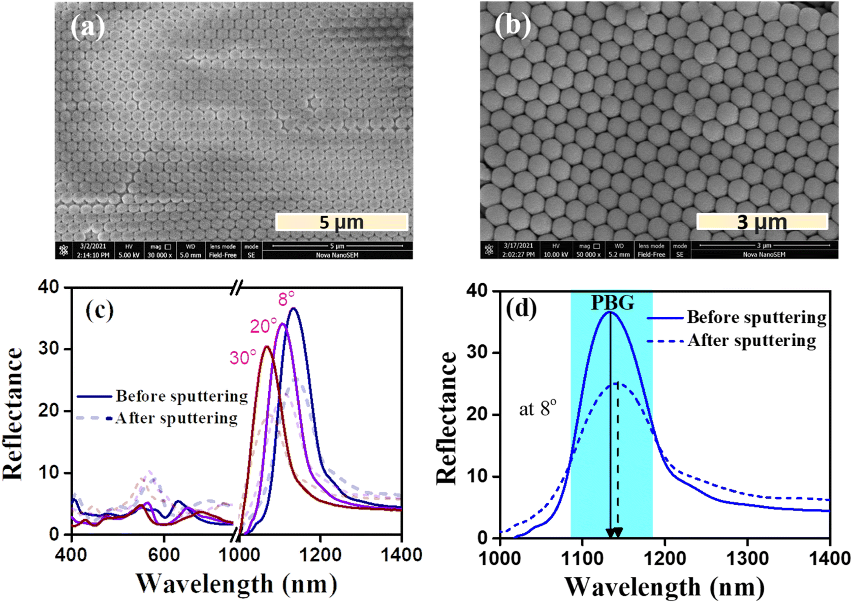 | ||
| Fig. 4 (a) SEM image showing periodic PS microspheres on glass, (b) SEM image of the CCO opal thin film, (c) angle-dependent reflectance spectra of opal and CCO opal on glass and (d) reflectance spectra at 8°, showing the PBG shift between opal and CCO opal. | ||
Periodicity of PhCs creates a region of forbidden energies commonly referred to as the photonic band gap (PBG).47 The PBG can be deduced from the reflectance spectrum of a PhC by giving the most intense peak where no light propagation is allowed. Many factors, such as RI, diameter, volume fraction, incident angle, etc., can be vital for determining the PBG position.48 The modified Bragg–Snell law49 gives the position of PBG at zero angle of incidence as follows:
| λ = 1.633d·neff | (1) |
Fig. 4(c and d) show the reflectance spectra of bare opal over glass and CCO over opal. For the opal thin film, the PBG was formed at 1133 nm for an incident angle of 8°. Also, the PBG shows a blue shift in the peak position with respect to the incident angle, which may be explained by the Bragg–Snell law at an angle of incidence θ given by,
 | (2) |
Upon depositing CCO, the PBG was shifted to 1144 nm for an incident angle of 8°. This may be due to the change in the neff of opal or the diameter of the PS spheres after depositing CCO. The incorporation of CCO has resulted in shifting the PBG to a higher wavelength by 11 nm. The neff was calculated from the y-intercept of λ2versus sin2(θ) using the Bragg–Snell law for opal on glass and CCO on opal/glass, which is plotted in Fig. S2(a).† The neff was found to be 1.42 and 1.41 for CCO opal and bare opal, respectively. The change in the slope of the two samples suggests that there was a slight change in the diameter of the PS sphere, which may have caused the increment in PBG positions. There was also a significant reduction in the intensity of PBG after depositing CCO on top of the opal. The formation of a thin layer of CCO on top of opal increased the absorption of light, thereby decreasing the intensity of PBG. Due to the absorption of light by CCO, the intensity of light passing to the opal can be lower compared to the initial intensity,44 which would result in a lower visible reflectance.
The gas sensing characteristics of the fabricated nanostructures were studied using an in-house built setup, as shown in Section 2.4, Fig. 3. Fig. 5(a) shows the change in the reflectance spectrum of CCO opal thin film after exposure to hydrogen gas mixed with nitrogen at various concentrations from 1% to 25%. The reflectance spectra were measured immediately after passing hydrogen for 20 min. Upon introducing hydrogen, the intensity of PBG decreases with the increase in the concentration of hydrogen gas. Fig. S2(b)† shows the ratio of the intensity of λPBG (I1105) to that of the background at 1800 nm (I1800). This ratio subsequently decreases with the concentration of hydrogen gas. The intensity of PBG depends upon factors such as the number of layers, periodicity, etc. In this case, where there was a CCO thin film coating over the opal, total reflectance is the result of interferences happening in the boundary as well as a change in neff, if any. Therefore, the intensity of the PBG is affected by the change in the composition of the thin film. In this case, it was the CCO layer, which was on top of the opal layer.
 | ||
| Fig. 5 (a) Reflectance spectra of CCO opal after exposure to different concentrations of hydrogen. The inset shows the same experiment with only PS opal without CCO. (b) In situ reflectance spectra of CCO opal when exposed to hydrogen gas. | ||
Exposure to hydrogen can reduce CCO to intermediate compounds with varying oxidation states. To understand the intermediate compound formed during hydrogen exposure, in situ reflectance measurements were also taken. Fig. 5(b) shows the change in reflectance spectra of the CCO opal thin film while passing 1% hydrogen in nitrogen. Measuring the reflectance spectrum in the hydrogen environment revealed that there is a shift in the PBG of the CCO opal thin film apart from the decrement of intensity, as observed previously.
The changes in the PBG and the intensity are plotted together in Fig. S2(c).† This figure shows that both the change in the PBG and the decrease in intensity occur within the first 10 minutes of exposure to the CCO opal film. Also, both attained saturation by 20 min, which can be considered as the response time of the CCO opal thin film for 1% H2–N2. After hydrogen exposure stopped, the PBG of the sample returned to its initial wavelength after approximately 20 minutes. However, the recovery of intensity took a longer time. To determine if this effect originated from the underlying opal layer, different concentrations of hydrogen gas were exposed to the sample with just the opal layer on a glass. The reflectance spectra are shown in the inset of Fig. 5(a), where no shift in the PBG was observed for the opal film. Also, the intensity change with the concentration of hydrogen was insignificant, as compared to the case of CCO opal. The same experiment was performed with a bare CCO thin film on a glass substrate, as shown in Fig. S2(d).† Here, a small reduction in intensity is observed with increasing hydrogen concentrations. This indicates that the neff change in CCO in the presence of hydrogen has more effect on CCO opal than bare CCO because even a small change in RI produces a shift in PBG. This confirms that the opal with a CCO layer on top acts as a better sensor than either the bare CCO or the opal thin film alone.
3.2 CCO-IO thin film
Another architecture of the fabricated PhC is the CCO inverse opal, as mentioned earlier. To obtain an ordered IO, the opal template used for electrodeposition should also be periodic, similar to the CCO opal. Also, since electrodeposition is a solvent-assisted method, there is a high chance of disintegration of PS in the electrolyte during the reaction. To avoid this, the opal template was sintered to bond the surfaces of two adjacent PS spheres, forming a neck.50 The SEM image of this self-assembled PS opal film is shown in Fig. S3(a).† It is visible from the figure that most of the PS spheres have formed necks between them.Forming a crack-free ordered CCO-IO by electrodeposition required optimization of several parameters, including deposition time, annealing rate, adhesion, etc.51 Compared to DC, PED resulted in a better IO structure, although it produced a thicker layer of CCO nanoflakes on top, as seen in Fig. 6(b). The thin film also adhered well to the substrate in the case of PED, compared to DC electrodeposition. Since the potential is periodically turned off in PED, as shown in Fig. 6(a), the metal layer may discharge, facilitating easier adsorption and re-distribution of metal ions.52 Also, during the ON time, nuclei formation occurs, and during the OFF time, recrystallization occurs, resulting in larger grains.52 This yields smoother, uniform surfaces, reducing rough and porous deposits, thereby increasing the adhesion of the film (see Fig. 6(b and c)).
 | ||
| Fig. 6 (a) The current profiles of DC vs. PED operation along with different stages of growth. The SEM images of the grown sample (b) with the template and (c) after removal of the template using slow, controlled heating. The bottom images show the top view of the sample. | ||
The magnified view of the CCO-IO film in the SEM image is shown in Fig. 7(a). As seen from Fig. 6(c), the periodic IO was covered with nanoflakes in most of the areas. The crystal structure of the CCO thin film formed by PED was confirmed by XRD, as shown in Fig. 7(b). The peaks at 36.9° and 38.9° in the XRD pattern correspond to (311) and (222) reflections of the CuCo2O4 spinel structure (JCPDS 066-0541). The three high-intensity peaks are due to nickel substrates. The extra peak at 35.5° in the XRD pattern corresponds to copper oxide (CuO) according to ICDD-01-073-6023. Like the CCO opal case, the CCO-IO thin film contains two phases, i.e., CCO and CuO. The low thickness and poor crystalline nature of CCO-IO led to poor XRD patterns. Therefore, Raman spectra of CCO-IO were acquired to further confirm the phase, which are shown in Fig. S3(b).† The Raman spectrum of the bare CCO thin film is also included for comparison. The Raman spectrum of the parent compound spinel Co3O4 has four vibration modes: 194 cm−1 (F2g), 480 cm−1 (Eg), 518 cm−1 (F2g), and 687 cm−1 (A1g).53 Out of which, peaks at 186 cm−1 (F2g), 463 cm−1 (Eg), 503 cm−1 (F2g), and 654 cm−1 (A1g) are observed for CCO. The shift to a lower frequency may be due to the structural disorder caused by metal doping.53 Small peaks at 282 cm−1 (Ag) and 325 cm−1 (B1g) correspond to Cu–O Raman active modes.54 This further confirms the presence of CuO along with CCO in the sample. Fig. S4(a)† shows the atomic percentages of each element of CCO-IO from SEM-EDS analysis. From the chemical formula for the spinel compound CuCo2O4, it is expected that typical Cu![[thin space (1/6-em)]](https://www.rsc.org/images/entities/char_2009.gif) :Co would have a 1:2 ratio. The excess Cu, in that case, is ascribed to the secondary phase of CuO, which was confirmed from XRD and Raman spectra.
:Co would have a 1:2 ratio. The excess Cu, in that case, is ascribed to the secondary phase of CuO, which was confirmed from XRD and Raman spectra.
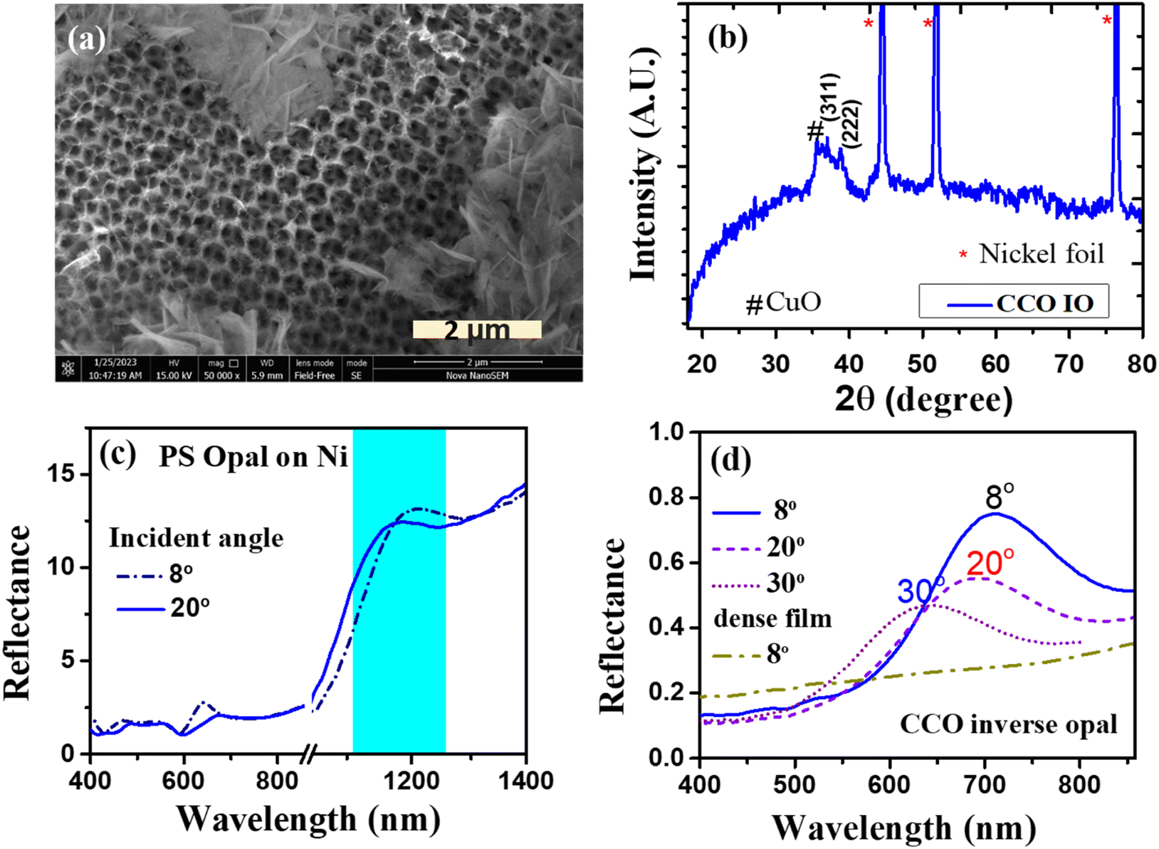 | ||
| Fig. 7 (a) SEM image of the CCO-IO thin film. (b) XRD pattern of the CCO-IO thin film on nickel foil. (c) Reflectance spectra of opal on nickel foil with different incident angles and (d) angle-dependent reflectance spectra of CCO-IO and bare CCO. | ||
To further probe the material crystal structure and the chemical composition, XPS analysis was done for CCO-IO. In CCO, Cu and Co occupy tetrahedral and octahedral sites, respectively, and may exhibit multiple oxidation states, as expected for a spinel crystal structure. Higher-order ternary spinel oxides typically crystallize in the form of (A1−yBy)[AxB2−x]O4−δ, where y is the fraction of B ions occupying A sites (tetrahedral) in the lattice and x is the fraction of A ions occupying B sites (octahedral) in the lattice.55 Fig. S4(b–d)† show the core-level spectra of Cu 2p, Co 2p, and O 1s, respectively.
In the Cu 2p core level spectra, multiple satellite peaks were observed between 2p1/2 and 2p3/2, indicating the presence of Cu2+ since Cu+ does not show satellite peaks.56 The Cu 2p3/2 peaks at 931.3 eV, 932.5 eV, and 934.1 eV correspond to octahedral Cu+, tetrahedral Cu+, and octahedral Cu2+, respectively, and similar trends were observed for the Cu 2p1/2 peaks.56 The enhanced intensity of the satellite peaks likely results from a higher concentration of Cu2+ ions that are beyond the solubility limit of Cu into the CuCo2O4 spinel structure. These excess Cu2+ ions may form CuO alongside CCO, as evidenced by additional peaks in the XRD pattern and Raman spectra.
The Co 2p core-level spectrum confirms the presence of Co2+ and Co3+ oxidation states, with binding energies corresponding to octahedral Co3+, tetrahedral Co2+, and a mixed formation of Co3+ and Co2+. The O 1s spectrum reveals two peaks: the lower binding energy peak corresponds to O2−, which is found in both CCO and CuO, while the higher binding energy peak is attributed to chemisorbed oxygen and lattice defects. Table S1† shows the peak maxima of Cu, Co, and O core-level resolved spectra. The presence of different oxidation states of Cu and Co in tetrahedral and octahedral coordination has been evident from the core-level XPS spectral analysis of Cu and Co. This confirms the formation of anti-site defects and leads to a chemical composition of (Cu1−yCoy) [CuxCo3−x]O4−δ to the final spinel crystal structure.
The PBG of the opal film on nickel foil was observed at 1190 nm for an incident angle of 8°, as shown in Fig. 7(c). The shift in the peak position in the reflectance spectrum with the incident angle confirmed the formation of the PBG and the ordered opal template. The reflectance peak was broader and lower in intensity compared to that of CCO opal on glass. This may be due to the non-uniform surface of the nickel foil, which causes cracks and smaller domains of periodicity over a large area. Fig. 7(d) shows the corresponding reflectance spectra of the CCO-IO. The peak corresponding to the PBG of CCO-IO is seen at about 700 nm for an incident angle of 8°. The shift of PBG of CCO-IO to a lower wavelength compared to that of the CCO opal thin film could be due to a change in neff. Since in the IO structure, a larger volume fraction is occupied by air (ni = 1), neff decreases as compared with the opal structure. Fig. 7(d) shows the reflectance spectrum of the dense CCO film for comparison, which does not show any peak in this region. This further confirms that the peak in the visible range was solely due to the periodic ordering in CCO-IO. Additionally, the peak shifted to a lower wavelength with an increase in the incident angle, which is a characteristic property of PhCs, as mentioned earlier. However, the intensity of the peak was very low, likely due to the layer of CCO nanoflakes formed on top of the IO and the lack of long-range periodicity, limited by cracks. Since the reflectance of the dense film is very low in the visible wavelength region, the absorption of visible light would be substantial.57 As a result, the intensity of light reflecting from the CCO-IO film could be lower.
As with the CCO opal thin film, the CCO-IO thin film was also exposed to various gases. The in situ reflectance spectrum was measured at an incident angle of 15° while passing hydrogen gas, as explained in the Experimental section. The PBG of CCO-IO was observed at 645 nm for an incident angle of 15°. When 1% hydrogen mixed with nitrogen was passed, the PBG position shifted to a lower wavelength of 633 nm, accompanied by a decrease in intensity at that wavelength, as seen in Fig. 8(a). The neff of CCO-IO, with and without hydrogen, was calculated using eqn (2), and it decreased by an amount of 0.0159 as the PBG shifted from 645 nm to 633 nm in the presence of 1% H2–N2. In the case of CCO opal, this shift was barely 5 nm, and the intensity change was also minimal compared to this case. The inverse opal is a more porous structure compared to the opal. This could, therefore, facilitate better diffusion of hydrogen gas into the sample.36 For CCO opal, the shift in the PBG and the change in intensity only occurred after 20 minutes, whereas in CCO-IO, it merely took 2 minutes response time when exposed to a 1% H2–N2 mixture under ambient conditions. To the best of our knowledge, this is the fastest response achieved for a photonic crystal optical hydrogen sensor without any catalyst at room temperature in the literature. The porosity leading to the increased surface area of CCO-IO could be a governing factor in decreasing the response time compared to CCO opal.58 To determine if the carrier gas (N2) contributed to this response, in situ reflectance measurements were taken with and without H2 in N2 conditions. First, the carrier gas (100% nitrogen) was passed, and once it saturated, 1% H2 was introduced in N2, and the response was measured during its passage, as shown in Fig. S5(a).† Here, the reflectance at PBG suddenly decreased in the presence of 100% N2, and then it saturated after some time. Subsequently, the reflectance decreased when 1% H2–N2 was passed. The sudden change in reflectance in the presence of 100% N2 could be due to the sudden change in the oxygen partial pressure of the environment.
 | ||
| Fig. 8 (a) In situ reflectance spectra of the CCO-IO thin film when exposed to hydrogen gas and (b) change in the intensity of reflected light over time for the film exposed to different concentrations of hydrogen. | ||
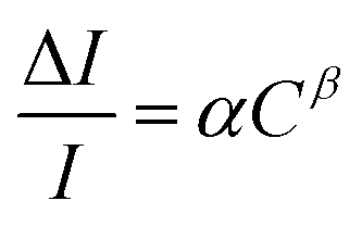
The sample was exposed to various concentrations of hydrogen mixed with synthetic air. The response of 1% H2–air is shown in Fig. S5(b–d).† The shift in wavelength, as well as the fall in the intensity, are similar to the case of H2–N2. Also, as may be seen from Fig. S5(d),† the recovery took a very long time in air (almost 30 minutes). It may be noted here that the test was not actively flushed during recovery; rather, it was allowed to diffuse by stopping the incoming H2–air mixture. This could contribute to the gas diffusion rate along with the sensors' inbuilt ability to recover when gas is completely removed. Subsequently, the response was measured for different concentrations of hydrogen by mixing it with synthetic air and directly exposing the sample to it under ambient conditions. This response is given in Fig. 8(b). This establishes that there is a monotonous change in the intensity with the concentration of hydrogen gas. Even though the gas was passed under ambient conditions, the change in the intensity follows the same trend. This further confirms the effect of hydrogen gas on the optical properties of the sample. The response curve was fitted with the power law, and the results are plotted in Fig. S5(e).† The sensor response, S, can be expressed as the fractional change in intensity, as given by eqn (3).
 | (3) |
The repeatability and selectivity studies for CCO-IO were performed to verify the sensor's compatibility. Fig. S6(a)† illustrates the repeatability of the sample's response to hydrogen gas. A consistent PBG shift of 12 ± 2 nm was observed over 200 days for CCO-IO in the presence of 1% H2 in Ar, demonstrating the excellent reproducibility of the sensor's response and the sample's repeatability.
Here, CCO-IO was exposed to another reducing gas, carbon monoxide (CO). 0.95% CO was injected by maintaining the partial pressure of O2 to the sample, and in situ reflectance spectra were measured, similar to the hydrogen exposure. The comparison of the responses to hydrogen and CO is shown in Fig. S6(b and c).† There was no significant shift observed in the PBG maxima of CCO-IO when exposed to CO, as seen in Fig. S6(b).† However, a slight decrease in intensity at the PBG was observed after injecting CO gas. This could be due to the changes in flow conditions, as no change in steady conditions was observed. Nevertheless, this intensity change was recorded over time, and as seen in Fig. S6(c),† the change in intensity was much smaller than that observed for hydrogen. These findings confirm the sensor's selective response to hydrogen gas.
3.3 In situ Raman studies and mechanism of response on the CCO-IO thin film
Raman spectroscopy is one of the best tools for understanding lattice vibrations and changes in local chemical bonding occurring in the material. The crystalline structure of CCO is either A[B]2O4 or B[AB]O4, representing normal or inverse spinel, respectively. Here, A and B can be divalent or trivalent metal ions, respectively. Also, the cations inside the bracket will be octahedrally coordinated with the oxide ion, whereas the one outside the bracket will be tetrahedrally coordinated in the lattice.42 The incorporation of copper into the parent spinel Co3O4 will result in altered lattice vibration modes and structural properties involving the mixed spinel structure or phase segregation of CuO.As mentioned before, the Raman spectrum of CCO consists of four major vibrational modes, similar to the parent compound Co3O4. In Co3O4, the Raman active modes correspond to the vibration of the Co–O bond in tetrahedral (CoO4) and octahedral (CoO6) coordination.59 The intense peak near 654 cm−1 is A1g due to the vibration of the Co–O bond in octahedral coordination, whereas the vibration at 186 cm−1 is the F2g mode arising due to the tetrahedrally coordinated CoO4 atoms. Additionally, two peaks at 463 and 503 cm−1 (Eg & F2g) represent a combined vibration from tetrahedral and octahedral architectures. Also, a shift to a lower frequency in the Raman spectra of CCO has been observed when compared with the parent structure, i.e., Co3O4. This is due to the incorporation of Cu into the Co3O4 lattice. Apart from these vibrations, Cu–O vibrations are also present, as mentioned earlier. This is also in accordance with the XRD, wherein an extra CuO phase is seen in the sample.
Fig. 9(a and b) show the in situ Raman spectra during exposure and recovery for 5% H2–Ar. During exposure to hydrogen, the spectra change drastically in terms of intensity of the Raman shift, as well as the peak positions. In the presence of hydrogen, the intensity of the F2g peak increases along with a shift of 20 cm−1 towards a higher value. A sudden change in the intensity was observed after about 3 minutes of exposure to hydrogen in the sample. The change in the A1g peak position to time during the exposure and recovery of 5% H2–Ar is shown in Fig. 9(c). The Raman spectra of CCO-IO after 10 min of exposure to hydrogen match exactly with those of the CoO phase, where a weak shoulder at 489 cm−1 and two prominent peaks at 540 and 680 cm−1, are identified as Eg, T2g, and A1g modes, respectively.60 Previously, laser-induced crystallization of CoO to Co3O4 was observed by B. Rivas-Murias et al., where it was found that the Raman peaks of CoO have evolved to Co3O4 with the increase of the laser power.59 Also, Co3O4 can be reduced to CoO in the presence of hydrogen at a temperature of 250 °C, as reported by Wang et al., where the structural transformation from the spinel lattice of Co3O4 to cubic CoO was confirmed by XRD, XPS, and XANES.61 Complete recovery of the Raman spectra was observed 70 minutes after stopping the hydrogen exposure. It may be noted that the response and the recovery time are similar to the optical sensing measurements.
 | ||
| Fig. 9 (a) In situ Raman spectra during the exposure of 5% H2–Ar, (b) in situ Raman spectra during the recovery from the exposure of 5% H2–Ar, (c) the response curve of the peak position while exposed to 5% H2–Ar and (d) the intensity ratio over time for different concentrations of hydrogen mixed with argon. | ||
Upon stopping the H2 flow, a new peak appeared at 212 cm−1, which matches with Cu2O vibrational modes.54 The formation of Cu2O as an intermediate compound can be due to the laser-induced crystallization and reduction of CuO, which was present along with the CCO-IO thin film.54 Noncrystalline CuO can crystallize to CuO with an intermediate Cu2O compound. Even though the laser power (1 mW) was lower compared to other studies, local heating may occur if the sample was exposed to a laser for a long time. This can eventually lead to local changes in the crystallinity of the thin film. Therefore, the formation of CoO and Cu2O as the intermediate compounds in the presence of hydrogen could be attributed to the origin of the PBG shift and intensity change observed during optical sensing. As described before, PBG shift in PhCs occurs due to the change in the RI between the actual and intermediate compounds. Here, it is clear that the formation of CoO can immediately result in a change in the RI of CCO-IO in the presence of hydrogen. Thus, there will be a shift in the PBG of CCO-IO. The A1g to F2g peak intensity ratio is plotted against time for different concentrations of H2–Ar in Fig. 9(d). As the concentration of hydrogen decreases from 5% to 0.5%, the response also decreases monotonously, whereas a similar trend was found in optical sensing. The recovery varied for different concentrations. Since, in this experiment, there was no forced 100% carrier gas flow to flush the chamber, the recovery was not controlled, and hence there is no definite trend for recovery with concentrations.
Fig. 10 shows the contour plot of the in situ Raman spectra with different hydrogen concentrations. Here, the intensity of Raman peaks is indicated by the color bar shown. Also, the color difference over time shows the change in the Raman peak intensity at a given wavenumber when exposed to hydrogen gas. As is seen from the intensity response curve, it is clear that the response decreases with the decreasing concentration (Fig. 10). For higher concentrations of hydrogen, after 6 minutes of exposure, the color of the F2g peak at 503 cm−1 becomes intense with respect to the A1g peak at 654 cm−1. While decreasing the concentrations, the intensity monotonously decreases. For 0.25% H2–Ar, there is no visible response to hydrogen.
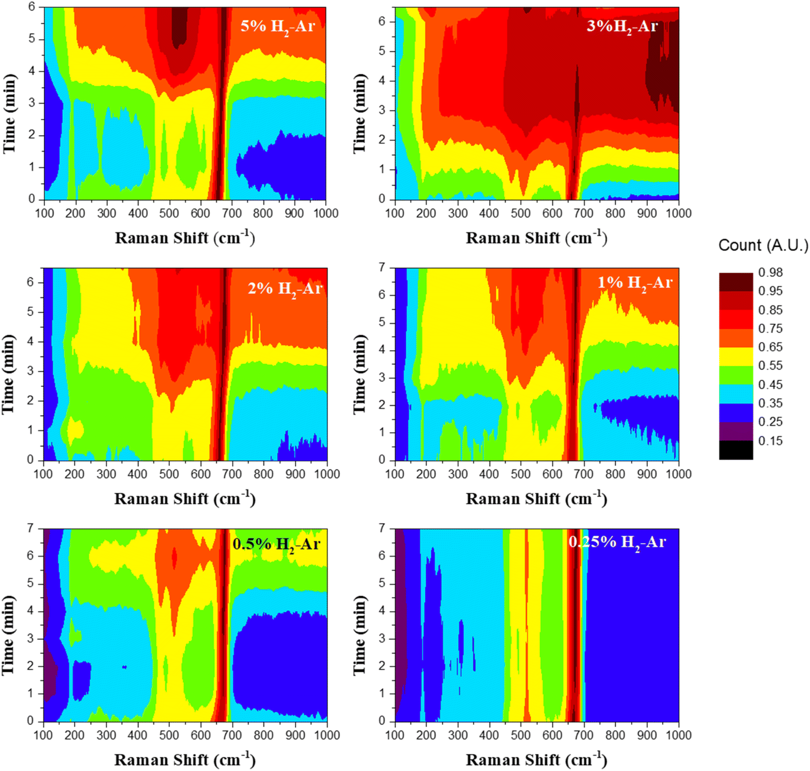 | ||
| Fig. 10 Contour plot of in situ Raman spectra of CCO-IO in the presence of different concentrations of hydrogen gas (concentrations are mentioned on each plot). | ||
The same experiment was repeated for an H2–N2 atmosphere, 100% O2, as well as 100% N2. The contour plots are shown in Fig. S7.† The H2–N2 mixture also shows a response towards hydrogen, but 100% O2 and 100% N2 do not show any response. This confirms that the response is solemnly due to hydrogen gas. The in situ Raman spectra could not be obtained for the CCO opal thin film due to its poor crystallinity, low thickness, and the presence of a PS template.
Comparing both optical sensing and in situ Raman spectra of CCO-IO, the change in PBG can be easily connected to the formation of intermediate reduced oxides. While optical sensing showed a shift in PBG in the presence of hydrogen, in situ Raman spectroscopic studies showed a shift in Raman peaks in the presence of hydrogen. When hydrogen was exposed to the porous CCO inverse opal, the vibrational modes of CCO changed to that of CoO, which has a different RI than that of CCO. This change in RI results in a change in the effective RI of the structure, hence the change in the PBG position. This caused the shift in the PBG in optical sensing. The same response time observed for both cases again proves that these changes can be inter-related.
4. Discussion
By exposing certain TMOs to hydrogen, the oxidation state of the metal ions can be reduced by the electrons donated by the intercalated hydrogenic species. CCO has a spinel crystal structure where various oxidation states of Cu and Co atoms are arranged in an octahedral and a tetrahedral geometry, as mentioned before. Often, anti-site defects exist wherein the cations exchange their positions.57 Under normal conditions, gases adsorbing on the surface lead to chemisorption or, at best, only change the surface chemical stoichiometry. However, the exposure of TMO can lead to a significant reduction of the oxide, leading to changes in optical properties such as dielectric constant, RI, and absorption of light (via a change in the bandgap).62,63 The in situ Raman spectroscopy performed in this work demonstrates that exposure of hydrogen to CCO not only results in the change of chemical (oxidation) states of the metal ions involved but also results in the change in the local crystal field of these cations with the ligand (oxide). This change in crystal symmetry leads to a change in the dielectric properties of the oxide.64 Similarly, the oxygen stoichiometry changes to compensate for the charge imbalance by creating or annihilating oxygen vacancies, leading to trapped charges, and thus a change in the oxygen vacancies contributes in a similar manner.65The change in the PBG position arises due to the difference in the RI of the reduced phase from that of the parent compound. The neff of a nanostructure can be calculated using eqn (4):
 | (4) |
5. Conclusion
Novel CCO PhCs with two different architectures, CCO opal and CCO inverse opal, were successfully fabricated and demonstrated for optical hydrogen sensing at room temperature without any noble element catalyst. CCO opal was fabricated by sputtering a CCO thin film on a self-assembled PS template on a glass substrate, whereas CCO-IO was fabricated by pulsed electrodeposition, leading to infiltration of CCO into a self-assembled PS template on nickel foil, followed by controlled annealing. Both CCO opal and CCO-IO resulted in periodic PhC structures with PBGs of 1144 nm and 700 nm, respectively, at an incident angle of 8°. The structure and morphology were confirmed by SEM images as well as their reflectance spectra for PBG estimation. The composition of both samples was confirmed to be CCO along with a secondary phase of CuO by XRD, Raman, and SEM-EDAX measurements.Optical sensing measurements were done mainly with dynamic reflectance measurements in the presence of different concentrations of hydrogen, which revealed a change in PBG and a decrease in the intensity at PBG for both samples. Even though CCO opal showed a response for a wide range of concentrations of hydrogen, the response time was found to be fairly large compared to other sensors. However, CCO-IO showed a response for various concentrations of hydrogen, with a response time as low as 120 seconds. Dynamic reflectance measurements were done for different combinations of hydrogen, like H2–N2 and H2–air. The change in intensity showed a decreasing behavior with a decrease in the concentration of hydrogen. Furthermore, to investigate the material interactions with gaseous molecules, in situ Raman spectra were obtained for CCO-IO with exposure to different gases, i.e., H2–Ar, H2–N2, O2, and N2. In situ Raman spectra showed a prominent change in the intensity as well as the peak position of the A1g and F2g peaks of CCO with a response time of 2–3 minutes in hydrogen environments. Also, just like the optical sensing measurements, a decrease in the intensity change was observed when the concentration of hydrogen was decreased. In the presence of hydrogen, the Raman spectra of CCO matched those of CoO, identified as the primary factor for the change in the PBG observed during the optical sensing. Also, no response was observed for gases like 100% N2 and 100% O2, which were present as diluting gases during sensing. Thus, in situ Raman spectra revealed the effect of hydrogen in CCO-IO, hence the origin of the sensing response in hydrogen. Moreover, our studies on two different PhCs of CCO have shown the possibility of using different architectures for optical hydrogen sensing at room temperature without the presence of any catalyst elements and also exploring the gaseous molecules' interactions with the material by in situ Raman spectroscopic studies.
Data availability
The data supporting this article have been included as part of the ESI.†Conflicts of interest
The authors declare the following financial interests/personal relationships which may be considered as potential competing interests: Indian Institute of Science Education and Research, Thiruvananthapuram, has obtained one Indian patent (Patent No. is 557307 and the grant date is 31/12/2024) on part of the technologies related to the optical hydrogen sensing described in this article. Most of the authors are listed as inventors on the patent applications.Acknowledgements
The authors are thankful to the SERB for the funding under the SERB Core Research Grant (CRG/2022/006973), and Ms Silpa would like to thank CSIR for the senior research fellowship. Ms Silpa would also like to thank Dr Soumya Biswas for his never-ending moral support and motivation during the project and Ms Athira S for her valuable input on the format of the manuscript. The authors would like to acknowledge a few alumni members of the lab whose contributions have led to the present work through various improvements in the process, namely Anupama T. Vasudevan, Anjana James, and Nithin P. Bharadwaj.References
- I. Staffell, D. Scamman, A. Velazquez Abad, P. Balcombe, P. E. Dodds, P. Ekins, N. Shah and K. R. Ward, Energy Environ. Sci., 2019, 12, 463–491, 10.1039/C8EE01157E.
- T. Hübert, L. Boon-Brett, V. Palmisano and M. A. Bader, Int. J. Hydrogen Energy, 2014, 39, 20474–20483, DOI:10.1016/j.ijhydene.2014.05.042.
- W. Buttner, M. Post, R. Burgess and C. Rivkin, Int. J. Hydrogen Energy, 2011, 36, 2462–2470, DOI:10.1016/j.ijhydene.2010.04.176.
- C. E. Antony, K. Gaana, S. G. Praveen, A. Jayakumar, A. Yadav, N. S. Sivakumar, N. Kamath, M. N. Suma, V. B. Kamble and D. Jaiswal-Nagar, ACS Appl. Nano Mater., 2021, 1643–1653, DOI:10.1021/acsanm.0c03109.
- G. Korotcenkov, S. Do Han and J. Stetter, Chem. Rev., 2009, 109, 1402–1433, DOI:10.1021/cr800339k.
- K. F. Chen, D. P. Yuan and Y. Y. Zhao, Opt. Laser Technol., 2021, 137, 106808, DOI:10.1016/j.optlastec.2020.106808.
- K. M. B. Urs, N. K. Katiyar, R. Kumar, K. Biswas, A. K. Singh, C. S. Tiwary and V. Kamble, Nanoscale, 2020, 12, 11830–11841, 10.1039/D0NR02177F.
- T. Hübert, L. Boon-Brett, G. Black and U. Banach, Sens. Actuators, B, 2011, 157, 329–352, DOI:10.1016/j.snb.2011.04.070.
- K. M. B. Urs, K. Sahoo, N. Bhat and V. Kamble, ACS Appl. Electron. Mater., 2022, 4, 87–91, DOI:10.1021/acsaelm.1c00912.
- Z. Li, H. Li, Z. Wu, M. Wang, J. Luo, H. Torun, P. Hu, C. Yang, M. Grundmann, X. Liu and Y. Fu, Mater. Horiz., 2019, 6, 470–506, 10.1039/C8MH01365A.
- Z. Zhang, X. Zou, L. Xu, L. Liao, W. Liu, J. Ho, X. Xiao, C. Jiang and J. Li, Nanoscale, 2015, 7, 10078–10084, 10.1039/C5NR01924A.
- Y. Yang, L. Yu, X. Jiang, Y. Li, X. He, L. Chen and Y. Zhang, Chem. Commun., 2024, 60, 9177–9193, 10.1039/D4CC01503G.
- S. Liu, M. Wang, Y. He, Q. Cheng, T. Qian and C. Yan, Coord. Chem. Rev., 2023, 475, 214882, DOI:10.1016/j.ccr.2022.214882.
- Y. Xu, P. Bai, X. D. Zhou, Y. Akimov, C. E. Png, L. K. Ang, W. Knoll and L. Wu, Adv. Opt. Mater., 2019, 7, 214909, DOI:10.1016/j.ccr.2022.214909.
- F. Zhou, S. J. Qiu, W. Luo, F. Xu and Y. Q. Lu, IEEE Sens. J., 2014, 14, 1133–1136, DOI:10.1109/JSEN.2013.2293347.
- E. Yablonovitch, Phys. Rev. Lett., 1987, 58, 2059–2062, DOI:10.1103/PhysRevLett.58.2059.
- S. John, Phys. Rev. Lett., 1987, 58, 2486–2489, DOI:10.1103/PhysRevLett.58.2486.
- Y. Zhang, Y. Zhao and R. Lv, Sens. Actuators, A, 2015, 233, 374–389, DOI:10.1016/j.sna.2015.07.025.
- G. von Freymann, V. Kitaev, B. V. Lotschz and G. A. Ozin, Chem. Soc. Rev., 2013, 42, 2528–2554, 10.1039/C2CS35309A.
- P. Wu, J. Wang and L. Jiang, Mater. Horiz., 2020, 7, 338–365, 10.1039/C9MH01389J.
- H. Xu, P. Wu, C. Zhu, A. Elbaz and Z. Gu, J. Mater. Chem. C, 2013, 1, 6087–6098, 10.1039/c3tc30722k.
- A. Mirzaei, J. H. Kim, H. W. Kim and S. S. Kim, Appl. Sci., 2019, 9, 1775, DOI:10.3390/app9091775.
- C. Gao, X. Guo, L. Nie, X. Wu, L. Peng and J. Chen, Int. J. Hydrogen Energy, 2023, 48, 2442–2465, DOI:10.1016/j.ijhydene.2022.10.100.
- N. T. Garavand, S. M. Mahdavi and A. I. Zad, Appl. Surf. Sci., 2013, 273, 261–267, DOI:10.1016/j.apsusc.2013.02.027.
- P. Castillero, V. Rico-Gavira, C. López-Santos, A. Barranco, V. Pérez-Dieste, C. Escudero, J. Espinós and A. González-Elipe, J. Phys. Chem. C, 2017, 121, 15719–15727, DOI:10.1021/acs.jpcc.7b03385.
- G. Gao, S. Xue, H. Wang, Z. Zhang, G. Wu, T. Debela and H. Kang, ACS Sustain. Chem. Eng., 2021, 9, 17319–17329, DOI:10.1021/acssuschemeng.1c06228.
- S. Xue, G. Gao, Z. Zhang, X. Jiang, J. Shen, G. Wu, H. Dai, Y. Xu and Y. Xiao, ACS Appl. Nano Mater., 2021, 4, 8368–8375, DOI:10.1021/acsanm.1c01557.
- D. Kulikova, A. Baburin, E. Lotkov, I. Rodionov and A. Baryshev, Int. J. Hydrogen Energy, 2024, 82, 767–775, DOI:10.1016/j.ijhydene.2024.07.458.
- F. X. Gu, H. P. Zeng, Y. B. Zhu, Q. Yang, L. K. Ang and S. L. Zhuang, Adv. Opt. Mater., 2014, 2, 189–196, DOI:10.1002/adom.201300413.
- F. A. A. Nugroho, I. Darmadi, V. P. Zhdanov and C. Langhammer, ACS Nano, 2018, 12, 9903–9912, DOI:10.1021/acsnano.8b02835.
- A. Sousanis and G. Biskos, Nanomaterials, 2021, 11, 3100, DOI:10.3390/nano11113100.
- C. Langhammer, E. Larsson, V. Zhdanov and I. Zoric, J. Phys. Chem. C, 2012, 116, 21201–21207, DOI:10.1021/jp3059273.
- J. S. Noh, J. M. Lee and W. Lee, Sensors, 2011, 11, 825–851, DOI:10.3390/s110100825.
- K. Chen, D. Yuan and Y. Zhao, Opt. Laser Technol., 2021, 137, 106808, DOI:10.1016/j.optlastec.2020.106808.
- A. K. Pathak, S. Verma, N. Sakda, C. Viphavakit, R. Chitaree and B. M. A. Rahman, Photonics, 2023, 10, 122, DOI:10.3390/photonics10020122.
- S. Amrehn, X. Wu and T. Wagner, ACS Sens., 2018, 3, 191–199, DOI:10.1021/acssensors.7b00845.
- Z. Xie, H. Xu, F. Rong, L. Sun, S. Zhang and Z. Gu, Thin Solid Films, 2012, 520, 4063–4067, DOI:10.1016/j.tsf.2012.01.027.
- A. Dey, Mater. Sci. Eng., B, 2018, 229, 206–217, DOI:10.1016/j.mseb.2017.12.036.
- K. Christmann, Prog. Surf. Sci., 1995, 48, 15–26, DOI:10.1016/0079-6816(95)93412-Z.
- J. Meyer, S. Hamwi, M. Kroger, W. Kowalsky, T. Riedl and A. Kahn, Adv. Mater., 2012, 24, 5408–5427, DOI:10.1002/adma.201201630.
- L. Kong, H. Chu, Z. Pan, S. Zhao and D. Li, J. Nonlinear Opt. Phys. Mater., 2024, 33, 2340005, DOI:10.1142/S0218863523400052.
- H. Behzad, F. E. Ghodsi and H. Karaagac, Ionics, 2017, 23, 2429–2442, DOI:10.1007/s11581-017-2081-2.
- E. Armstrong and C. O’Dwyer, J. Mater. Chem. C, 2015, 3, 6109–6143, 10.1039/C5TC01083G.
- S. Silpa, G. Srinivas, A. Biswas, H. C. Barshilia and V. B. Kamble, Adv. Opt. Mater., 2023, 2300567, 10.1039/C5TC01083G.
- L. Abbasi and M. Arvand, Appl. Surf. Sci., 2018, 445, 272–280, DOI:10.1016/j.apsusc.2018.03.193.
- Y. Xiong, F. Kang, Z. Ke, S. Zhuo, C. Liang and Z. Zhang, J. Cryst. Growth, 2010, 312, 2484–2488, DOI:10.1016/j.jcrysgro.2010.05.029.
- E. Yablonovitch, Sci. Am., 2001, 285, 46, DOI:10.1038/scientificamerican1201-46.
- W. Zhang, J. Min, H. Wang, H. Wang, X. Li, S. Ha, B. Zhang, C. Pan, H. Li, H. Liu, H. Yin, X. Yang, S. Liu, X. Xu, C. He, H. Yang and J. Yang, Nat. Nanotechnol., 2024, 19, 1813–1820, DOI:10.1038/s41565-024-01780-5.
- E. Armstrong and C. O’Dwyer, J. Mater. Chem. C, 2015, 3, 6109–6143, 10.1039/C5TC01083G.
- B. Hatton, L. Mishchenko, S. Davis, K. Sandhage and J. Aizenberg, Proc. Natl. Acad. Sci. U. S. A., 2010, 107, 10354–10359, DOI:10.1073/pnas.1000954107.
- N. Sapoletova, T. Makarevich, K. Napolskii, E. Mishina, A. Eliseev, A. van Etteger, T. Rasing and G. Tsirlina, Phys. Chem. Chem. Phys., 2010, 12, 15414–15422, 10.1039/c0cp00812e.
- B. H. Juárez, C. López and C. Alonso, J. Phys. Chem. B, 2004, 108, 16708–16712, DOI:10.1021/jp047475n.
- X. Chen, S. C. Cai, E. Q. Yu, J. J. Li, J. Chen and H. P. Jia, Appl. Surf. Sci., 2019, 484, 479–488, DOI:10.1016/j.apsusc.2019.04.093.
- W. Bodeau, K. Otoge, W. Yeh and N. Kobayashi, ACS Appl. Mater. Interfaces, 2022, 460–466, DOI:10.1016/j.jallcom.2015.09.119.
- S. Joshi, V. Kamble, M. Kumar, A. Umarji and G. Srivastava, J. Alloys Compd., 2016, 654, 460–466, DOI:10.1016/j.jallcom.2015.09.119.
- A. Amri, Z. T. Jiang, P. A. Bahri, C. Y. Yin, X. L. Zhao, Z. H. Xie, X. F. Duan, H. Widjaja, M. M. Rahman and T. Pryor, J. Phys. Chem. C, 2013, 117, 16457–16467, DOI:10.1021/jp404841m.
- A. James, P. Pradeep, H. Barshilia and V. B. Kamble, J. Appl. Phys., 2020, 127, 145303, DOI:10.1063/1.5143348.
- T. Wang, I. Can, S. Zhang, J. He, P. Sun, F. Liu and G. Lu, ACS Appl. Mater. Interfaces, 2018, 10, 5835–5844, DOI:10.1021/acsami.7b19641.
- B. Rivas-Murias and V. Salgueiriño, J. Raman Spectrosc., 2017, 48, 837–841, DOI:10.1002/jrs.5129.
- U. Wdowik and K. Parlinski, Phys. Rev. B: Condens. Matter Mater. Phys., 2007, 75, 104306, DOI:10.1103/PhysRevB.75.104306.
- X. Wang, Y. Liu, T. Zhang, Y. Luo, Z. Lan, K. Zhang, J. Zuo, L. Jiang and R. Wang, ACS Catal., 2017, 7, 1626–1636, DOI:10.1021/acscatal.6b03547.
- M. Feng, J. Li, S. Zhang, A. Pofelski, R. El Hage, C. Klewe, A. N’diaye, P. Shafer, Y. Zhu, G. Galli, I. Schuller and Y. Takamura, J. Phys. Chem. C, 2024, 128, 17124–17133, DOI:10.1021/acs.jpcc.4c04098.
- E. Kondoh, M. Fukasawa and T. Ojimi, J. Vac. Sci. Technol., A, 2007, 25, 415–420, DOI:10.1116/1.2712197.
- T. Fernandez, K. Privat, M. Withford and S. Gross, Sci. Rep., 2020, 10, 15142, DOI:10.1038/s41598-020-72234-w.
- W. Li, J. Shi, K. Zhang and J. MacManus-Driscoll, Mater. Horiz., 2020, 7, 2832–2859, 10.1039/D0MH00899K.
Footnotes |
| † Electronic supplementary information (ESI) available. See DOI: https://doi.org/10.1039/d4ta08963d |
| ‡ These authors contributed equally. |
| § Present address: Nonlinear Nanophotonics (NLNP), University of Twente, Drienerlolaan 5, 7522 NB Enschede, Overijssel, Netherlands. |
| This journal is © The Royal Society of Chemistry 2025 |