
 Open Access Article
 This Open Access Article is licensed under a
 Creative Commons Attribution 3.0 Unported Licence
Critical metal recovery from e-waste in concentrated ionic media using ultrasound†
Christopher E.
Elgar
 *,
Kelsey
Hall
and
Andrew P.
Abbott
*,
Kelsey
Hall
and
Andrew P.
Abbott
Centre for Sustainable Materials Processing, School of Chemistry, University of Leicester, Leicester, LE1 7RH, UK. E-mail: cee17@leicester.ac.uk
First published on 12th March 2025
Abstract
With an increase in the amount of e-waste being generated worldwide, there is greater demand for sustainable recycling techniques to recover components and technology critical metals (TCMs) that would otherwise be discarded. Current methods for solder removal are inefficient, produce harmful gases and by-products. This work aims to use catalytic etchants in concentrated ionic media, to improve the sustainability of recycling techniques. The viscosity of these solutions is often perceived as a limiting factor for ion mobility, so ultrasonic agitation has been used to improve mass transport. Cyclic voltammetry and linear sweep voltammetry have been used to investigate the redox behaviour of tin and lead in solder, and how ultrasound can overcome passivation and improve the dissolution of these metals. Ultrasound results in a linear response between the slope of the LSV and solution conductivity for tin, suggesting a migration-controlled mechanism, however passivation still occurred with lead, showing that there is still some diffusion control. A waste printed circuit board was etched using FeCl3 catalyst in a choline chloride and ethylene glycol DES (ChCl![[thin space (1/6-em)]](https://www.rsc.org/images/entities/char_2009.gif) :2EG) but no major components were removed after 30 minutes of sonication at room temperature. The use of a choline chloride and water in a 1:10 molar ratio removed most of the components, along with some gold coating, under the same conditions. The additional water content in the brine improved the fluidity of the solution, enabling dissolution of the solder and copper under-layer, freeing the gold. Cavitation effects including acoustic streaming and jetting work in tandem to aid metal removal.
:2EG) but no major components were removed after 30 minutes of sonication at room temperature. The use of a choline chloride and water in a 1:10 molar ratio removed most of the components, along with some gold coating, under the same conditions. The additional water content in the brine improved the fluidity of the solution, enabling dissolution of the solder and copper under-layer, freeing the gold. Cavitation effects including acoustic streaming and jetting work in tandem to aid metal removal.
Sustainability spotlightThe increased need for a low carbon society brings together a significant demand on material resources, as well as generating substantial amounts of new waste streams. The e-waste levels are only expected to increase and consumer electronics markets grow. While traditional e-waste recycling, such as shredding followed by pyro-, and hydrometallurgy methods allow for the recovery of these critical materials, the process is long and energy intensive. The use of ultrasound coupled with deep eutectic solvents and concentrated ionic brines allows for the recovery of the critical materials at room temperature. This work emphasizes the importance of the following UN sustainable development goals: industry, innovation, and infrastructure (SDG 9), responsible consumption and production (SDG 12) and climate action (SDG 13). |
1. Introduction
Waste Electrical and Electronic Equipment (WEEE) is a priority waste stream due to the severity of four major factors: the global amount of WEEE generated, the impacts this has on resources, concerns regarding people's health and the environment, and ethical issues.1 The management of WEEE waste channels is a cause for concern, as such the Right to Repair legislation in the UK2 and the EU,3 or the European Union (EU) directive introduced in 2012 aimed to improve the management of e-waste.4WEEE levels fluctuate, e.g. with the COVID-19 pandemic and the work from home trend.5 Printed Circuit Boards (PCBs) account for approximately 3 wt% of electronic scraps and around 70% are unable to be efficiently recycled due to the complexity of their structure.6
One of the main issues with recovering technology critical metals from WEEE is the prevalence of solders which create electrical connections between components. Historically, the most commonly used solder is a Sn–Pb alloy in a 60:40 wt% ratio,7,8 however the toxicity of lead9 has resulted in the move towards Pb-free solder alternatives.10 Mass produced PCBs are generally produced via wave soldering11 or reflow soldering12 where in both cases solder pads are pre-soldered to attach electrical components.
With the demand for technology critical metals (TCMs) increasing alongside the generation of WEEE globally, it is important to consider how the role of recycling and recovery can be utilised to provide a more sustainable approach. Sustainability will help the supply and demand issue, as well as put less strain on the environment. Recovery of TCMs from PCBs has mostly focussed on the recovery of gold13 with pre-treatment methods vital for the enrichment of metal valorisation.14 Removal of electrical components is typically done in one of three ways; manual or mechanical dismantling,15,16 thermal treatment,17 or dissolution of solder using strong acids.18,19 Waste PCBs (WPCBs) can then be treated via bioleaching, hydro- or pyro-metallurgical methods to recover the remaining TCMs.20
There has been much interest in using Deep Eutectic Solvents for the recovery of TCMs from WPCBs. Zhao et al. used a 2-stage leaching process for the treatment of mixed metal oxides left from dismantled and crushed WPCBs. By first leaching in a choline chloride (ChCl) and glycolic acid (GA) DES, followed by a ChCl-oxalic acid DES, the authors were able to separate Zn in the first leach followed by the formation of Sn and Cu oxalates in the second, with the copper species precipitating via the addition of water.21
By combining DESs, made from either CaCl2·6H2O and ethylene glycol in a 1:1 ratio, or ChCl and ethylene glycol (ChCl:2EG) with an earth abundant oxidant, such as FeCl3 or CuCl2, it has been shown to selectively target the copper tracks underpinning the gold, allowing for the gold be recovered from solutions.22,23 One of the main drawbacks to using DESs is the increase in viscosity over conventional solvent processes. To overcome this, previous studies have shown that a concentrated aqueous brine can be used for metals that do not passivate in aqueous solutions.24 FeCl3 or CuCl2 are chosen for their efficiency in the oxidation of copper, while exhibiting chemical reversibility and low costs. However, the FeII/III redox couple exhibits a more stable potential with varying water content than CuCl2, as seen by water addition to DES and in different ChCl brines.24
The main downside to using a DES is the increase in viscosity over traditional lixiviants, which in turn lowers the rates of mass transport. One potential way of increasing mass transport is employing the use of forced convection via the use of ultrasound. Sound waves propagating through the solution causes the formation of microbubbles. As the sound causes alternating high- and low-pressure waves, the microbubbles begin to shrink and expand until they reach a critical size, and implode.25 This violent implosion is known as cavitation, and sends shock waves through the solution. These shockwaves can cause acoustic streaming, leading to mixing of the local environment, allowing for increased mass transport rates. Secondly, if cavitation occurs next to a surface, the cavitation occurs asymmetrically, sending a forceful jet into the surface, acting as a physical disruption to the surface.26
The use of ultrasound has been shown to increase the rates of mass transport for WPCB recycling in DESs.27 Targeted high-powered ultrasound can remove the gold from WPCBs in under 5 minutes using 0.1 mol dm−3 FeCl3 as a redox etchant, as opposed to 8 hours under silent control.23
Dissolution of solder in aqueous solutions can cause SnO passivation layers.28 This can be prevented through the use of an ultrasonic 40 kHz bath, allowing for the complete dissolution of the solder. Ultrasound has also been shown to greatly improve the yield of lead recovery from landfill residues in an acidic sodium chloride solution.29 Recovery was improved by up to 26% with an 8-fold decrease in the time needed for processing over silent conditions.
The aim of the current study is to rapidly etch solder using a catalytic redox agent enabling recovery of critical elements and release of components from the printed circuit board.
2. Experimental
2.1 Reagents and solvent preparation
All chemicals were used as supplied. The ChCl:2EG DES solution was prepared from 1 mol eq. of choline chloride (Honeywell, >98%) and 2 mol eq. of ethylene glycol (Fisher Scientific, 98%). Brines were prepared by the addition of choline chloride (Honeywell, >98%) in deionised water (Elga Purelab Option apparatus) at varying molar ratios of salt-to-water (1:3, 1:5, 1:10, and 1:20). The solvents were prepared by stirring the components at 60 °C until a colourless homogeneous liquid was formed. The solvent was removed from the heat and stored at room temperature in sealed storage bottles. To limit the effects of variations in water content, the same batch of ChCl:2EG was used throughout this work. Solutions containing oxidising agents were prepared by dissolving 0.5 mol dm−3 of iron(III) chloride (Acros Organics, 99%) in the relevant solvent. Solutions containing PbCl2 (Aldrich, 98%) and SnCl2·6H2O (Sigma Aldrich, 98%) were prepared by dissolving 0.01 mol dm−3 in the relevant solvent.
2.2 Instrumentation
The electrochemical behaviour of the target metals was studied by cyclic voltammetry (CV), using an IVIUMnSTAT potentiostat. A 0.5 mm diameter platinum disk was used as the working electrode, with a platinum flag counter electrode, and a 3.0 mol dm−3 KCl Ag/AgCl reference electrode. Solder CVs were measured using a working electrode made from 60/40 Sn–Pb solder wire (RS Pro, UK. Diameter 0.71 mm), set in coldset resin (Metprep, UK), with a platinum flag counter electrode, and a 3.0 mol dm−3 KCl Ag/AgCl reference electrode. Prior to each experiment, the working electrode was polished with a 0.3 μm and 0.05 μm alumina slurry, rinsed with deionised water, and air dried. The reference electrode potential was calibrated to the [Fe(CN)6]3–/4– redox couple, which is used as an internal standard to ensure comparability between the different solvents. The scan rates were 10 to 100 mV s−1.Anodic linear sweep voltammetry (LSV) experiments were performed at 20 °C, using a Metrohm Autolab PGStat302N potentiostat, together with the corresponding Nova 2.1 software. A 3-electrode set-up was used, consisting of a hooked Sn (diameter 1 mm) or Pb (area 0.027 cm2) disc working electrode, a tin or lead wire quasi-reference electrode (corresponding to the working electrode), and an IrO2 coated Ti mesh as a counter electrode. The LSVs were recorded at scan rates between 5 and 100 mV s−1. Prior to use, electrodes were polished on 800 grit, 1200 grit, and finally 2400 grit sandpaper (Metprep, UK). For the LSV experiments with ultrasound, a 20 kHz commercial ultrasonic system from Fisherbrand was used, connected to a CL-334 ultrasonic probe (diameter: 13 mm) operating with power variable up to 700 W (527 W cm−2). For these experiments, the ultrasonic horn was placed at a distance of 4 mm above the working electrode. The experiments were carried out in 200 mL of solvent at 20 °C. Ultrasound was applied during the whole period that the anodic scan lasted.
Surface morphology and elemental were measured with a Quanta FEG 650 scanning electron microscope (SEM) (ThermoFisher Scientific, USA) equipped with an XMax energy dispersive X-ray spectroscopy (EDX) (Oxford Instruments, UK), and an accelerating voltage of 20 kV at the University of Leicester's Advanced Microscopy Facility.
Tornado M4 Plus μXRF manufactured by Bruker, Germany. The conditions were as follows: Rh tube, 50 kV, 600 μA.
2.3 Etching of PCBs
Etching of solder from PCB boards was studied by using a PCB test coupon that had undergone hot air levelled solder coating, using a 60:40 Sn/Pb solder. PCBs were kindly provided by Anotech UK, with PCB containing components coming from a camera circuit taken from an end-of-life CAT S62 pro mobile phone, kindly supplied by the Bullitt Group. PCB samples were placed into a vial containing 10 mL solvent with iron(III) chloride oxidising agent. Samples were run with no agitation for 30 minutes at room temperature (20 °C), stirring at 200 rpm for 30 minutes at room temperature or sonication in a Fisherbrand FB15055 ultrasonic bath, operating at 38 kHz, for 10 minutes. Etch rate was determined by capturing 3D optical topographical images of the sample as a function of time by using a Zeta Instruments Zeta 200 optical profiler using the inbuilt Zeta3D software version 1.8.5. Images were constructed by determining the features of an image that are in focus at different heights, resulting in a 3D topographical map of the surface.
3. Results and discussion
3.1 Electrochemistry of leaded solder
Fig. 1 shows linear sweep voltammograms (LSVs) for Sn, Pb and a 60:40 wt ratio of Sn and Pb. It also shows a cyclic voltammogram for 0.5 mol dm−1 FeCl3 in ChCl:2EG. It can be seen that the redox potential for the FeIII/II couple is more positive than any of the metal samples showing that they should all etch in an FeCl3 in ChCl:2EG solution. The current density for Sn dissolution is much larger than that for Pb and similar to that for solder showing that the rate of solder dissolution is controlled by the dissolution of Sn. Fig. 1b shows that the open circuit potential for Sn and Pb electrodes in 0.5 mol dm−3 FeCl3 in ChCl:2EG is at approximately −0.2 V and does not change significantly with time until the point when the ultrasonic horn is switched on (*). At this point there is a significant increase in the open circuit potential which presumably occurs due to the fast rate of metal etching and the knock-on effect that this has on the cell potential via the Nernst equation.
 | ||
| Fig. 1 (a) LSV curves for Sn, Pb and solder working electrodes recorded in ChCl:2EG at 10 mV s−1. Included cyclic voltammogram for 0.5 mol dm−3 FeCl3 in ChCl:2EG recorded at 10 mV s−1. Remaining measurements were made using 0.5 mol dm−3 FeCl3 in ChCl:2EG (b) Chronopotentiometry for Sn and Pb electrodes recorded at 0 A. Chronoamperometry for Sn (c) and Pb (d) electrodes recorded at OCP (−0.608 V and −0.198 V respectively vs. [Fe(CN)6]3−/4−). Green asterisks indicated when sonication was initiated (130 W cm−2). | ||
Fig. 1c and d show the current density of the tin and lead electrodes in 0.5 mol dm−3 FeCl3 in ChCl:2EG at the open circuit potential. The decrease in current density under silent conditions is expected as the dissolution process is diffusion controlled. When the ultrasonic horn is switched on (*) there is a rapid increase in current density which must occur due to an increase in surface area resulting from the rapid etching.
Fig. 2 shows the response for the same electrodes in a 1:10 ChCl:H2O brine. It can clearly be seen that the same trends occur in the brine solutions but the current densities are higher due to the lower solution viscosity and increased mass transport. The higher on-set potential for Pb oxidation is also observed in the differences in the OCP for Sn and Pb in Fig. 2b. We have previously shown that DESs have similar properties to brines and in many cases, it is just mass transport which increases in the brine due to lower viscosities.24
 | ||
| Fig. 2 (a) LSV curves for Sn, Pb and solder working electrodes recorded in 1:10 ChCl brine at 10 mV s−1. Included cyclic voltammogram for 0.5 mol dm−3FeCl3 in 1:10 ChCl brine recorded at 10 mV−1. (b) Chronopotentiometry for Sn and Pb electrodes recorded at 0 A in 0.5 mol dm−3 FeCl3 in 1:10 ChCl Brine. (c and d) Chronoamperometry for Sn (c) and Pb (d) electrodes recorded at OCP (−0.608 V and −0.198 V respectively vs. [Fe(CN)6]3−/4−). Green asterisks indicated when sonication was initiated (130 W cm−2). | ||
The (electro)dissolution of metals in DESs and brines has previously been studied with the assistance of ultrasound. This is the first study of the dissolution of a heterogeneous alloy. The two liquids studied will have different viscosities and solubilities for the two metallic components. It was previously shown for copper dissolution that the linear region of the LSV was linearly correlated to the conductivity of the solution and it was suggested that under the conditions of forces mass transport ionic migration was limiting the rate of dissolution.30Fig. 3 shows that the same linear correlation between solution conductivity and the LSV slope was observed for both lead and tin in a range of ChCl brines and ChCl:2EG. The difference in slope between lead and tin is probably due to the difference in ionic size and charge of the solution species. While speciation of metals in DESs has been studied31,32 the speciation in brines is less well studied. Previous studies showed significant differences in the speciation of Cu(II), Co(II) and Ni(II) in DESs and brines33 but these are difficult to quantify for Sn and Pb due to the lack of absorbance in the visible region.
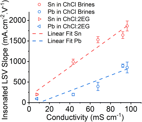 | ||
| Fig. 3 Slope of insonated LSVs for lead and tin working electrodes, recorded in varying molar ratios of a ChCl brines (1:3, 1:5, 1:10 and 1:20) and ChCl:2EG versus the solution conductivity. Individual LSVs for each solvent can be found in Fig. S4†. | ||
3.2 Dissolution of solder
In the silent experiments there is a more marked difference in the dissolution current between Sn and Pb due presumably to the low solubility of Pb in solution. Insonated experiments showed a smaller difference in the behaviour of the two metals.Given that the rate of dissolution of tin and lead are different it could be expected that solder being a heterogeneous alloy containing a solid solution of tin in lead (α) and lead in tin (β) would etch in an anisotropic manner. It would be expected that the β phase would dissolve faster than the α phase. To test this idea, solder samples were etched in 0.5 mol dm−3 FeCl3 in ChCl:2EG in an ultrasonic bath for 30 s to aid mass transport and decrease passivation. The results from this etching experiment are shown in Fig. 4. It can clearly be seen that even after a very short etch time (30 s) the β phase is significantly more etched than the α phase. It is assumed that the β phase dissolves around the α phase. This leads to two main benefits when recycling anisotropic alloys. Firstly, anisotropic etching around one phase preferentially means that we can use a lower concentration of oxidant to get the same result as if the whole alloy was etching separately. Secondly, in the case of leaded solder, it allows for the separation of the valuable tin from the toxic lead. As will be shown later, this results in a lead rich residue after bulk dissolution of the solder.
 | ||
| Fig. 4 (a) SEM SE, (b) EDS map for Pb (red) and Sn (blue), and (c) 3D topography for solder surface after etching for 30 seconds (0.5 mol dm−3 FeCl3 in a 1:10 ChCl brine) in ultrasonic bath. | ||
Hot air solder levelling (HASL) coated PCB test coupons were used to study chemical etching of the Sn/Pb solder. The test coupons were etched in 0.5 mol dm−3 FeCl3 for different lengths of time. Firstly, the coupons were characterised using SEM and EDX microscopy, and for each etching time point the surface was measured using 3D optical tomography microscopy. Fig. 5 shows a cross section from a HASL PCB test coupon, where the major component of the electrical tracks is copper.
 | ||
| Fig. 5 SEM cross section of PCB HASL test coupons used in this study. Test coupon was mounted in a conducting resin to allow for SEM cross section. Image recorded in BSE mode, with an accelerating voltage of 20.00 kV. | ||
The copper is 13.1 ± 1.4 μm thick layer, while the solder layer on top is 5.2 ± 0.8 μm thick. Between the solder and the copper layer a thin 1.2 ± 0.2 μm intermetallic layer has formed from the migration of copper into the tin layer, likely during the soldering process. The solder layer consists of areas of intense tin phases and areas of high Pb content, indicated by the brighter spots on the BSE image due to the heavier Pb centre. This can also be seen in the EDX elemental maps shown in Fig. 4.
A kinetic study of PCB etching rates was carried out using 0.5 mol dm−3 FeCl3 in two liquids: ChCl:2EG and 1:10 ChCl brine in an ultrasonic bath to increase mass transport. Sample coupons were imaged using a Zeta 20 3D optical microscope to get a baseline reading. Each block was then placed into a sample vial with ChCl:2EG. Fresh boards were placed into each solution for different lengths of time, and then imaged using 3D microscopy to track the changes in morphology and etch depth as a function of time. To ensure the etch depth measured was consistent, the fibreboard was taken as the base height as this will not change in the experiments, and then an average was taken of the step height between the board and the soldered area. An example of how this data was collected can be found in Fig. S5.†
Fig. 6 shows the appearance of the samples as a function of time. In ChCl:2EG it takes about 6 min before the copper substrate becomes visible and 8 min before it is totally removed. In 1:10 ChCl brine all of the solder has been removed in about 30 s. This suggests that the etch rate in 1:10 ChCl brine is approximately 15 times faster than in ChCl:2EG. This is approximately the ratio of the open circuit current for tin in Fig. 1 and 2 suggesting that for the etching of solder, tin dissolution is rate determining.
 | ||
| Fig. 6 2D images taken to show the progression of etching vs. time for 0.5 mol dm−3 FeCl3 in (left) ChCl:2EG and (right) 1:10 ChCl brine, with a leaded HASL test coupon. Inset graph showing the etch depth, calculated from the average step height between the fibreboard and the soldered area, as a function of time for 0.5 mol dm−3FeCl3 in ChCl:2EG, and 1:10 ChCl brine with ultrasonic agitation at 25 °C. | ||
Fig. 6 inset shows the etch depth of the samples as a function of time. It can be seen that in 1:10 ChCl brine an approximately linear increase in etch depth is observed with time whereas in ChCl the etch rate slows with time suggesting that the higher viscosity may lead to partial passivation due to the decrease in accessible tin phase and the proliferation of insoluble lead phase.
3.3 Electronic component removal
Although perfect test boards are good for investigating how these etchants can facilitate the dissolution of solder, they are not a true representation of what will realistically be recycled. The process of removing solder using the solutions was repeated using PCB samples with components that had been recovered from end-of-life (EoL) smartphones. The sample in Fig. 7 was a camera circuit taken from an end-of-life CAT S62 pro mobile phone, kindly supplied to the EPSRC funded Met4Tech project by the Bullitt Group. | ||
| Fig. 7 PCB of a camera circuit taken from EOL CAT S62 pro mobile phone images showing the PCB samples before etching (a) after 30 minutes of sonication in 0.5 mol dm−3 FeCl3 in ChCl:2EG at 25 °C (b) and 30 minutes of sonication in 0.5 mol dm−3 FeCl3 in 1:10 ChCl brine at 20 °C (c). The filter paper post-vacuum filtration for the solutions after 30 minutes of etching in 0.5 mol dm−3 FeCl3 in ChCl:2EG (d) and 1:10 ChCl brine (e). | ||
The components are attached to the board via soldered pads, rather than traditional legs. These PCBs work via solder pads where there are areas of exposed copper in which solder can be applied and the components placed on top to secure them in place. Therefore, if the solder can be dissolved, the components should also be removed with ease as there are no legs that may prevent the ECs from being taken off.
For these trials, the 0.5 mol dm−3 FeCl3 in the ChCl:2EG and 1:10 ChCl brine were used to compare their performance on real electronic samples. In practice, the etching of the samples took longer than the 8 minutes or 30 seconds that would be expected from the above experiments for the two etchants because the solder layers are thicker and the electronic components will hinder transport to the solder pads. As expected, 1:10 ChCl brine was fester etching than ChCl:2EG and small components were seen to float from the board after 5 minutes and larger components being removed in around 10 min. In ChCl:2EG however, smaller components were not seen in less than 10 min.
The final images of the boards after 30 minutes total of etching can be seen in Fig. 7. The ChCl:2EG board is still relatively intact with a few small components removed, however the brine board is missing a large amount of its original features, especially the larger components. In addition, the majority of the gold coating had also been removed. Gold is only a minor component of PCBs making up ≪1% by mass but represents >98% of the value of recoverable metal.
Overall, the ChCl:2EG struggled to remove the Au compared to the brine. The Au on the edge of the boards has been removed, however there is an area in the middle of the board that has been entirely untouched. This is a consequence of the solution etching into the Cu layer underneath which consequently results in the removal of Au from the surface. Ultrasound combined with the higher fluidity of the brine allows the ions to migrate to and from the Cu layer underneath and etch more efficiently than the DES. There is no access to the Cu for the Au section in the centre of the board, explaining why this Au cannot be removed.
The solution post-etch was filtered using vacuum filtration and Fig. 7 shows the clear differences between the two: the brine was successful in removing more components than the DES, as well as removal of Au. The brine can ‘undercut’ the ECs more efficiently and reach the solder mounts due to the increased fluidity, which has been one of the most important factors throughout the experiments. XRF analysis of the brine filter paper can be seen in Fig. 8, with additional maps in Fig. S6.† Pb and Sn emission lines appear at very similar energies and therefore the maps for each element are likely to contain contributions from both elements. Since the filter paper was rinsed after filtration with DI water, the solubility of PbCl2 would decrease, causing precipitation to occur in the filter paper. Otherwise, the dark precipitate seen on the filter papers in Fig. 7 appear to be a mix of copper chlorides, copper oxide, and (oxo)hydroxide nickel species. Since the FeCl3 was used in excess as the oxidant, it is also appearing all over, despite the rinsing with deionised water. This is seen in the optical images as the filter paper is stained a characteristic orange colour.
 | ||
| Fig. 8 X-ray fluorescence data for the 1:10 ChCl brine filter paper. (a) Filter paper as scanned (b) XRF spectrum of the filter paper. (c–f) Elemental maps of the filter paper for Au, Cu, Ni and Cl respectively. | ||
A de-soldering process to remove components such as capacitors, chips, transistors and resistors, which are known to contain other TCMs, such as rare earth elements is advantageous through a simple chemical processing that also allows for the separation and recovery of TCMs such tin and gold from the PCB fibreboard, which can be run for 0.067 kW h kg−1 of WEEE processed (see ESI†). This process allows simple separation via sorting by size using sieves to allow concentration of different waste streams before moving on with further processing. This removes the need for pre-processing stages such as manual EC stripping or shredding before the metal recovery can begin.
4. Conclusions
In this study, the dissolution of solder from waste printed circuit boards has been investigated, using FeCl3 as the oxidising agent in concentrated ionic media, including a DES and chloride brines. Cyclic voltammetry was used to characterise the redox chemistry of the base metals, tin and lead, and the effect of fluidity and conductivity on dissolution rates. Solutions with higher conductivity and higher fluidity resulted in higher dissolution rates. Linear sweep voltammetry with and without ultrasound showed a migration-controlled process under high powered ultrasound and diffusion control under lower powered ultrasound.Using FeCl3 as the oxidising agent showed etching times of around 30 seconds in 1:10 ChCl:H2O brine, compared to 8 minutes in ChCl:2EG. to remove the solder layer from HASL test coupons. Applying this approach to PCBs from waste mobile phones enabled the 1:10 ChCl brine to remove electronic components after as little as 5 minutes, with almost all components being removed after a 30 min when low powered ultrasound was used. However, the etchant containing the ChCl:2EG DES struggled to remove even the smallest components after the same 30 minute time frame, which was to be expected from the initial dissolution studies. This study has shown that Earth abundant redox catalysts can be used to recover electronic components and technology critical metals from waste electronic scrap samples. The use of brines will ensure that the process is both cost-effective and sustainable.
Data availability
Data available from corresponding author on reasonable request.Author contributions
Christopher E. Elgar – investigation, formal analysis, supervision, visualisation, writing – original draft, writing – review & editing. Kelsey Hall – investigation, formal analysis, writing – original draft. Andrew P. Abbott – conceptualisation, supervision, funding acquisition, writing – original draft, writing – review & editing.Conflicts of interest
There are no conflicts of interest to declare.Acknowledgements
The authors would like to thank the Engineering and Physical Sciences Research Council (EPSRC) Sonocat project (EP/W018632/1), and the UKRI Interdisciplinary Circular Economy Centre for Technology Metals, Met4Tech project (EP/V011855/1) for funding this work. We also acknowledge the University of Leicester Advanced Microscopy Facility for providing the microscopy suite and Dr Rachel Armitage at the University of Leicester Advanced Microanalysis facility access, funded by the AHRC Capabilities and Collections Scheme (AH/V011634/1) – Remaking materials: Upgrade of Archaeological Material Labs in School of Archaeology & Ancient History (SAAH).References
- O. S. Shittu, I. D. Williams and P. J. Shaw, Waste Manage., 2021, 120, 549–563 CrossRef PubMed.
- Ecodesign for Energy-Related Products and Energy Information Regulations 2021 No. 745, 2021.
- Proposal for a Directive of the European Parliament and of the Council on common rules promoting the repair of goods and amending Regulation (EU) 2017/2394, Directives (EU) 2019/771 and (EU) 2020/1828, 2023.
- Directive 2012/19/EU of the European Parliament and of the Council of 4 July 2012 on waste electrical and electronic equipment (WEEE) (recast) (Text with EEA relevance), 2018.
- D. E. C. Yu, K. D. S. Yu and R. R. Tan, Clean. Respons, Consump., 2020, 1, 100005 CrossRef.
- M. Kaya, Waste Manage., 2016, 57, 64–90 CrossRef CAS PubMed.
- L. R. Garcia, W. R. Osório, L. C. Peixoto and A. Garcia, J. Electron. Mater., 2009, 38, 2405–2414 CrossRef CAS.
- K.-K. Xu, L. Zhang, L.-L. Gao, N. Jiang, L. Zhang and S.-J. Zhong, Sci. Technol. Adv. Mater., 2020, 21, 689–711 CrossRef CAS PubMed.
- Directive 2011/65/EU of the European Parliament and of the Council of 8 June 2011 on the restriction of the use of certain hazardous substances in electrical and electronic equipment (recast) (Text with EEA relevance), 2014.
- P. J. McGuiness and R. Ogrin, Securing Technology-Critical Metals for Britain: Ensuring the United Kingdom's Supply of Strategic Elements & Critical Materials for a Clean Future, University of Birmingham, Birmingham, 2021 Search PubMed.
- M. Arunasalam, Z. B. Leman, B. T. H. T. B. Baharudin, S. B. Sulaiman and C. S. Anthony Das, Int. J. Precis. Eng. Manuf. - Green Technol., 2022, 9, 645–660 CrossRef.
- L. Ran, D. Chen, C. Chen and Y. Gong, Processes, 2023, 11, 2716 CrossRef CAS.
- H. Duan and X.-N. Zhu, Energy Sources, Part A, 2022, 44, 1640–1659 CrossRef.
- S. Mir and N. Dhawan, Resour., Conserv. Recycl., 2022, 178, 106027 CrossRef CAS.
- R. Khanna, P. S. Mukherjee and M. Park, J. Cleaner Prod., 2020, 268, 122319 CrossRef CAS.
- S. Arya, A. Patel, S. Kumar and S. Pau-Loke, Environ. Pollut., 2021, 283, 117033 CrossRef CAS PubMed.
- S. Park, S. Kim, Y. Han and J. Park, Int. J. Miner. Process., 2015, 144, 11–15 CrossRef CAS.
- X. Zhang, J. Guan, Y. Guo, Y. Cao, J. Guo, H. Yuan, R. Su, B. Liang, G. Gao, Y. Zhou, J. Xu and Z. Guo, Environ. Prog. Sustainable Energy, 2017, 36, 873–878 CrossRef CAS.
- A. Chaurasia, K. K. Singh and T. R. Mankhand, Int. J. Metall. Eng., 2013, 2, 243–248 Search PubMed.
- E. Schwartz, H. He, K. Frost, B. H. Nguyen, O. A. Ogunseitan and J. M. Schoenung, J. Hazard. Mater., 2024, 134545 CrossRef CAS PubMed.
- Q. Zhao, S. Ma, W. Ho, Y. Wang, J. Y. T. Ho and K. Shih, J. Cleaner Prod., 2023, 421, 138508 CrossRef CAS.
- R. M. Rivera, G. Zante, J. M. Hartley, K. S. Ryder and A. P. Abbott, Green Chem., 2022, 24, 3023–3034 RSC.
- B. Jacobson, S. Li, R. Marin Rivera, P. Daly, C. E. Elgar, D. M. Mulvihill, A. P. Abbott, A. Feeney and P. Prentice, Ultrason. Sonochem., 2023, 101, 106701 CrossRef CAS PubMed.
- G. Zante, C. E. Elgar, K. George, A. P. Abbott and J. M. Hartley, Angew. Chem., Int. Ed., 2023, 62, e202311140 CrossRef CAS PubMed.
- S. Bao, B. Chen, Y. Zhang, L. Ren, C. Xin, W. Ding, S. Yang and W. Zhang, Ultrason. Sonochem., 2023, 98, 106525 CrossRef CAS.
- J. Klima, Ultrasonics, 2011, 51, 202–209 CrossRef CAS.
- R. M. Rivera, C. E. Elgar, B. Jacobson, A. Feeney, P. Prentice, K. Ryder and A. P. Abbott, RSC Sustainability, 2024, 2, 403–415 RSC.
- P. Zhu, J. Tang, Q. Tao, Y. Wang, J. Wang, Z. Li, Z. Cao, G. Qian, F. Theiss and R. L. Frost, Environ. Eng. Sci., 2019, 36, 1236–1243 CrossRef CAS.
- J. J. John, V. De Houwer, D. Van Mechelen and T. Van Gerven, Ultrason. Sonochem., 2020, 69, 105239 CrossRef CAS.
- C. E. Elgar, S. Ravenhill, P. Hunt, B. Jacobson, A. Feeney, P. Prentice, K. S. Ryder and A. P. Abbott, Electrochim. Acta, 2024, 476, 143707 CrossRef CAS.
- I. M. Pateli, A. P. Abbott, G. R. T. Jenkin and J. M. Hartley, Green Chem., 2020, 22, 8360–8368 RSC.
- J. M. Hartley, C.-M. Ip, G. C. H. Forrest, K. Singh, S. J. Gurman, K. S. Ryder, A. P. Abbott and G. Frisch, Inorg. Chem., 2014, 53, 6280–6288 CrossRef CAS PubMed.
- E. Daskalopoulou, P. Hunt, C. E. Elgar, M. Yang, A. P. Abbott and J. M. Hartley, Faraday Discuss., 2024, 253, 329–342 RSC.
Footnote |
| † Electronic supplementary information (ESI) available. See DOI: https://doi.org/10.1039/d4su00715h |
| This journal is © The Royal Society of Chemistry 2025 |