
 Open Access Article
 This Open Access Article is licensed under a
 Creative Commons Attribution 3.0 Unported Licence
Molecular mobility of thin films of poly(bisphenol-A carbonate) capped and with one free surface: from bulk-like samples down to the adsorbed layer†
Hassan
Omar
 a,
Shayan
Ahmadi
a,
Paulina
Szymoniak
a and
Andreas
Schönhals
*ab
a,
Shayan
Ahmadi
a,
Paulina
Szymoniak
a and
Andreas
Schönhals
*ab
aBundesanstalt für Materialforschung und –prüfung (BAM), Unter den Eichen 87, 12205 Berlin, Germany. E-mail: Andreas.Schoenhals@bam.de; Fax: +49 30/8104-73384; Tel: +49 30/8104-3384
bInstitut für Chemie, Technische Universität Berlin, Straße des 17. Juni 135, 10623 Berlin, Germany
First published on 4th December 2024
Abstract
The molecular mobility of thin films of poly(bisphenol A carbonate) (PBAC) was systematically investigated using broadband dielectric spectroscopy, employing two distinct electrode configurations. First, films were prepared in a capped geometry between aluminum electrodes employing a crossed electrode capacitor (CEC) configuration, down to film thicknesses of 40 nm. The Vogel temperature, derived from the temperature dependence of relaxation rates of the α-relaxation, increases with decreasing film thickness characterized by an onset thickness. The onset thickness depends on the annealing conditions, with less intense annealing yielding a lower onset thickness. Additionally, a broadening of the β-relaxation peak was observed with decreasing thickness, attributed to the interaction of phenyl groups with thermally evaporated aluminum, resulting in a shift of certain relaxation modes to higher temperatures relative to the bulk material. A novel phenomenon, termed the slow Arrhenius process (SAP), was also identified in proximity to the α-relaxation temperature. For films with thicknesses below 40 nm, nanostructured electrodes (NSE) were utilized, incorporating nanostructured silica spacers to establish a free surface with air. This free surface causes an enhancement in the molecular mobility for the 40 nm sample, preserving the β-relaxation as a distinct peak. The α-relaxation was detectable in the dielectric loss down to 18 nm, shifting to higher temperatures as film thickness is decreased. Notably, the onset thickness for the increase in Vogel temperature was lower in the NSE configuration compared to the CEC setup, attributed to the presence of the polymer–air interface.
Introduction
Recently, thin polymer films with thicknesses below 100 nm have become of significant technological importance due to different material properties compared to the bulk and reduced production costs. They have been employed in a wide variety of applications such as coatings, organic light emitting diodes, porous membranes, microelectronics, and adhesives1–3 to mention a few. Interactions between polymer segments and the substrate as well as the increasing influence of confinement effects are assigned as the cause for the change in properties. For thin films, for instance, properties such as wetting, diffusion, the thermal glass transition temperature (Tg), and the glassy dynamics can deviate from those of the bulk.4–10The dependence of Tg on the thickness of thin films has been extensively studied for a variety of polymers where contradicting results have been reported. Keddie et al.11 discussed a decrease of Tg with decreasing film thickness for poly(methyl methacrylate) (PMMA) on a gold substrate whereas for PMMA on silicon a slight increase of Tg was observed. For polystyrene (PS), a decrease in the Tg was reported as the film thickness was reduced using ellipsometry12,13 and fluorescence spectroscopy14 as well as dielectric expansion dilatometry.15 However, using a dynamic technique like alternating current (AC)-chip calorimetry16 or dielectric spectroscopy where a dynamic Tg,dyn is measured (see for instance15,17,18), Tg,dyn (glassy dynamics) was found to be independent of film thickness. Nevertheless, using dielectric spectroscopy Fukao19 also reported no change of the glassy dynamics down to a critical film thickness (dc), where for film thicknesses, d, below this critical value Tg,dyn decreases strongly with further decreasing of d. Aside from the behavior of polymers with a flexible backbone, the thickness dependence of thin films of mainchain polymers has also been studied. For instance, investigations of thin films of polysulfone (PSU) reported both a decrease and an increase of Tg with a reduction in film thickness.9,20–24 Therefore, more investigations are required to elucidate this phenomenon for thin films of mainchain polymers.
The origin for the complex dependence of the thermal and dynamic glass transition temperature on the film thickness for supported thin films was attributed to the existence of a solid interface and a free surface at the polymer/air interface. The resulting interactions and geometrical constraints imposed on the polymer confined in thin films compared to the bulk25,26 can be discussed in the frame of an idealized three-layer model.8 On the one hand, the presence of a free surface results in an increased mobility for polymer segments located at the polymer/air interface due to missing segment–segment interactions. This effect will cause a decrease in the Tg. On the other hand, for polymer segments having non-repulsive interactions with a solid interface, an irreversibly adsorbed layer with a reduced mobility is formed at the substrate that leads to an increase in Tg.27,28 The segments located in the middle of the film retain properties similar to a bulk sample. The value of Tg for the whole thin film is then assumed to be a complicated average of all these effects. For further details refer to ref. 8 and 29.
The investigation of the irreversibly adsorbed layer has become an important topic due to its influence on the macroscopic properties of thin films. The adsorption process was investigated using the method initially proposed by Guiselin30 for solutions. This process was adopted for thin films by spin-coating a polymer solution onto a substrate to prepare a film with thickness between 100–200 nm. Upon annealing the obtained film at temperatures above Tg, polymer segments will adsorb onto the surface. The so-called Guiselin brushes are obtained upon rinsing the thin film with a good solvent after annealing. As a result of this procedure, only the adsorbed chains remain on the substrate forming the adsorbed layer.25 The growth kinetics for the adsorbed layer have been previously studied for several polymers including PS31,32 and poly(2-vinyl pyridine) (P2VP).33,34 Reviews into the solvent leaching process and the adsorbed layer including several polymers can be found elsewhere.35,36 A two-step growth mechanism was observed for polymers with a flexible backbone. At short annealing times the thickness of the adsorbed layer grows linearly with time. For longer annealing time the growth kinetics changes to a logarithmic time dependence due to the crowding of segments at the surface of the substrate. In the first regime a tightly bound adsorbed layer is formed consisting mainly of trains where in the second regime a loosely bound adsorbed layer is formed where loops and dangling end are present. From the existence of trains, it is expected that the structure of the chains in the adsorbed layer is highly asymmetric. For mainchain polymers, poly(bisphenol-A carbonate) (PBAC)37 and polysulfone (PSU)24 a more complicated growth process was found. At annealing times shorter than characteristic for the linear growth a pre-growth regime was evidenced. This additional step was attributed to an increased rigidity of the mainchain, where bulky groups like aromatic rings are present, compared to more flexible polymers which can orient parallel to the substrate and stack. Additionally, the adsorbed layer of PBAC showed signs of dewetting at long annealing times and higher temperatures. For PSU such indications of dewetting were not observed.
Investigations to study the behavior of thin films by broadband dielectric spectroscopy have been performed previously on various polymer systems (see for instance8,15,38–42). However, for mainchain polymers, such as PBAC or PSU, only few studies on the thickness dependence of the thin film properties are available in the literature. Currently, only dielectric studies of thin films of PSU and PBAC capped between two aluminum electrodes have been reported.9,43 The molecular mobility of thin films supported on a substrate with a polymer air interface, or the adsorbed layer remains largely unstudied for this class of polymers. The behavior may differ from that of simpler polymers such as poly(2-vinylpyridine) (P2VP)44 and poly(vinyl methyl ether) (PVME)45 where investigations of semi-isolated chains of P2VP or the adsorbed layer of PVME exist. Thus, for the investigation considered here, the mainchain polymer PBAC was selected. Two different electrode configurations were employed to study the molecular mobility of thin and ultrathin PBAC films, with one free surface and with capped ones. In addition, the adsorbed layer obtained by a solvent leaching approach, was also studied by dielectric spectroscopy.
Materials and methods
PBAC, with a molecular weight of 24![[thin space (1/6-em)]](https://www.rsc.org/images/entities/char_2009.gif) 400 g mol−1 and PDI and of 1.88, was obtained from Sigma Aldrich (Germany). The chemical structure of PBAC is shown in the inset of the right part of Fig. 1. The glass transition temperature of bulk PBAC was estimated to 411 K by differential scanning calorimetry (heating rate 10 K min−1, second heating run).37 It is worth to mention that the glass transition temperature of the PBAC employed in ref. 43 was estimated to 426.2 K (15 K higher).
400 g mol−1 and PDI and of 1.88, was obtained from Sigma Aldrich (Germany). The chemical structure of PBAC is shown in the inset of the right part of Fig. 1. The glass transition temperature of bulk PBAC was estimated to 411 K by differential scanning calorimetry (heating rate 10 K min−1, second heating run).37 It is worth to mention that the glass transition temperature of the PBAC employed in ref. 43 was estimated to 426.2 K (15 K higher).
 | ||
| Fig. 1 (left) AFM topography image of a ca. 170 nm thick film, the red line indicates a profile taken across the film surface. (right) The thickness profile along the red line given in the left side of the figure. The inset shows the chemical structure of poly(bisphenol-A carbonate) (PBAC). | ||
From the molecular weight a radius of gyration can be calculated from the freely rotating chain model and considering a characteristic ratio C∞ of 9.5.46 The relatively high value of C∞ points to a relative stiff chain structure of PBAC This calculation results in a radius of gyration of 48 nm.
Diluted solutions were prepared by dissolving the PBAC pellets in dichloromethane (DCM) in different concentrations to obtain films with different thicknesses. The solutions were first filtered using a PTFE syringe filter then spincoated onto the different substrates (see below). The thickness of each film was measured after spin coating and annealing at 443 K for 72 h. The film was scratched down to the surface of the substrate using a clean blade. The height of the scratch was measured by scanning the topography between the film and the substrate by AFM. The image was analyzed using the software Gwyddion.47Fig. 1 depicts an AFM image of a ca. 170 nm thick film of PBAC with a profile taken across the surface.
Film casting of bulk PBAC
A bulk sample of PBAC for the dielectric measurement was obtained by film casting a concentrated PBAC solution into a disk-shaped mold. The mold was placed at ambient temperature for three days into a closed chamber where its atmosphere is saturated with the vapor of the solvent to allow for a slow initial evaporation of DCM. For a complete evaporation of the solvent, the film was then annealed at 443 K for 72 h in an oil-free vacuum. Circular Al electrodes with a diameter of 15 mm were thermally deposited in an ultrahigh vacuum (10−5 mbar) on both sides of the bulk film. The film with a thickness of 100 μm was measured in a parallel plate capacitor geometry.Contact angle
Contact angle measurements were carried out for PBAC and the SiO2 as well as the Al substrates using an automated contact angle system (Krüss, Hamburg, Germany). The contact angles were measured by the static sessile drop method. Diiodo-methane, ethylene glycol, glycerol, and water were employed as test liquids.Crossed electrode capacitors (CEC)
Glass slides (10 × 10 mm) were cleaned in an ultrasonication bath with a water solution at 333 K for 15 min, then rinsed with acetone and then in ultra highly purified water with an alkaline cleaner. Next, the glass substrates were washed with acetone and chloroform and then dried with compressed air. An aluminium strip with a width of 2 mm and a height of 60 nm was deposited in ultrahigh vacuum onto the glass slide. This bottom electrode had a relative high roughness of 2.6 nm. Then 25 μL of the PBAC solution were pipetted on the glass substrate and spin-coated on top of the aluminium strip. The parameters for spin-coating were: 10 s with a rotational speed of 6500 rpm and an acceleration of 3000 rad s−2 followed by 50 s, with 8000 rpm and 3000 rad s−2. For the estimation of the thicknesses of the prepared films see above. After annealing the film at T = 443 K for 72 h a second strip of aluminium was deposited perpendicular oriented to the first one. During the evaporation process a polymer metal interface is formed.48 To minimize the influence of this interface on the dielectric properties of the film the evaporation time was kept as short as possible. The crossing area of the aluminium strips defines the capacitor for the dielectric measurements. The film between the two electrode strips can be considered as a capped. The samples were investigated by BDS employing isothermal frequency scans. The second heating run was used for analysis.Nanostructured electrodes (NSE)
The second used electrode configuration was nanostructured electrodes.44 The nanostructured electrode system was purchased from Novocontrol (Germany, Montabaur, NanoKit). The highly doped conductive SiO2 bottom wafers (4 × 8 mm) and nanopatterned SiO2 wafers (1 × 1 mm) were first washed with acetone to remove the protective layer on the top of the surface. The wafers were then dried with compressed air and treated using a plasma cleaner with an oxygen atmosphere (60 W, 600 s). Lastly, the wafers were cleaned using super critical CO2 obtained by a jet nozzle. The 4 × 8 mm wafer served as the substrate for the film. The surface roughness of this SiO2 wafer is less than 1 nm. Here films with thicknesses of 40 nm and below were prepared by spincoating onto the bottom electrode. The same parameters for spincoating and annealing conditions described above for the preparation of the CEC were used. The top electrode (1 × 1 nm), which has insulating silica spacers at the surface with a height of 60 nm, was placed onto the surface of the sample to allow the film to have a free surface with air. This sample geometry is also referred to as supported thin films.Solvent leached samples
The adsorbed layer sample (AL) was prepared from a film with a thickness of 200 nm spincoated onto cleaned 4 × 8 mm SiO2 substrates. The sample was then annealed in an oil-free vacuum at T = 443 K for 72 h. After annealing, the film was soaked in DCM for 20 minutes to remove all non-adsorbed polymer chains. This procedure was followed by a further rinsing of the sample with DCM. Lastly, after annealing at T = 443 K for an additional 20 minutes the adsorbed layer sample was prepared. For details the reader is referred to ref. 37.Broadband dielectric spectroscopy (BDS)
Dielectric measurements were performed using a high resolution Novocontrol Alpha analyser with an active sample cell and a Quatro temperature controller. The stability of the sample temperature was 0.1 K. Isothermal frequency scans were carried out in the frequency range from f = 10−1 to 106 Hz at temperatures between 200 to 503 K. A periodic electric field with low strength (VRMS = 0.1 V) adapted to the thickness of the sample was applied and the complex dielectric function ε*(ω) = ε′(ω) − iε′′(ω) was measured. Here ε′(ω) is the real (storage) part of the complex dielectric function and ε′′(ω) is the imaginary (loss) part. denotes imaginary unit and ω is the angular frequency with ω = 2πf.
Results and discussion
Interfacial energy
The properties of the thin films of PBAC are influenced by the different interactions of the polymer segments with the different substrates. Therefore, the interfacial energy between the different substrates, Al for CEC as well as SiO2 for NSE, and PBAC was estimated by calculating the surface tension for each material from contact angle measurements. Contact angle measurements were conducted using diiodo methane, ethylene glycol, glycerol, and water as test liquids. An average of 2–6 contact angles were taken for each test liquid. Table S1 in the ESI† lists the estimated contact angle values for each substrate materials and PBAC. The total surface tension of these materials is considered as the sum of their dispersive (γLW, Lifshitz-van der Waals (LW) interactions) and polar components (γP), γTotal = γLW + γP. The surface tension for the test liquids was taken from ref. 49 in the form of the γLW and γP values. The Owens–Wendt–Rabel and Kaelble (OWRK) method50,51 was used to estimate the surface tension values for PBAC, SiO2 and Al. Using this method, the measured contact angle, and polar and dispersive parts of the surface tension of the test liquid were converted into the reduced coordinates given below: | (1) |
 | (2) |
| Material | γ Total [mJ m−2] | γ LW [mJ m−2] | γ P [mJ m−2] |
|---|---|---|---|
| PBAC | 18.1 ± 0.2 | 15.9 ± 0.1 | 2.2 ± 0.1 |
| Al | 29.6 | 28.8 | 0.8 |
| SiO2 | 37.1 ± 2.6 | 30.3 ± 1.3 | 6.8 ± 1.3 |
Crossed electrode capacitors
A detailed study about the behavior of thin films of PBAC capped between two Al electrodes has been reported elsewhere.43 In the investigation presented here, one aim was to study the influence of the annealing conditions and thereby the thickness of the adsorbed layer on the glassy dynamics of thin PBAC films. Accordingly, the study presented in ref. 43 was extended by considering a different annealing condition Tg,Bulk + 30 K (443 K) for 72 h. In ref. 43 the samples were annealed at Tg + 17 K (443 K) for 24 h. Moreover, the influence of the film thickness on the localized fluctuations was considered in more detail compared to ref. 43.Thin films of PBAC, with thicknesses of 170 nm, 130 nm, 75 nm, 60 nm, 48 nm, 45 nm, and 40 nm, were prepared in the CEC arrangement, as described in the materials section. From the calculated radius of gyration, it is concluded that the global chain structure is highly asymmetric and stretched for the thinnest films. Fig. 2 shows a comparison of the dielectric loss for bulk PBAC and a thin film with a thickness of 170 nm versus temperature at a fixed frequency of f = 103.5 Hz. As known from the literature, the dielectric spectra show different dielectric active processes, which are assigned in Fig. 2. At low temperatures a broad peak is observed for both the bulk sample and the thin film. This process is denoted as β-relaxation and assigned to localized fluctuations of the polymer segments. The molecular origin of this process will be discussed in detail below. Secondly, at higher temperatures than characteristic for the β-relaxation, the α-relaxation (dynamic glass transition, glassy dynamics) is observed. The α-relaxation is due to the cooperative segmental motions. For the thin film there seems to be an additional contribution to the dielectric loss in the temperature range between 350 K and 400 K which is not present for the bulk. The origin of this contribution is discussed in detail below.
 | ||
| Fig. 2 The dielectric loss versus temperature at a frequency f = 103.5 Hz for bulk PBAC and a film with a thickness of 170 nm. The green line indicates the β-relaxation, and the orange line indicates the α-relaxation. The spectra are shifted along the y-scale for sake of clearness. | ||
The dielectric loss data for bulk PBAC and the thin film samples were analyzed by fitting the Havriliak–Negami (HN) model function to the dielectric loss. The HN function describes the symmetric and asymmetric broadening of a relaxation peak compared to the Debye function. The HN function is given by the following equation.54,55
 | (3) |
 | (4) |
 to the imaginary part of the HN-function.56 Here σ0 is related to the DC conductivity of the system but might include also parasitic effects like electrode polarization. The parameter s ≤ 1 describes non-ohmic effects in the conductivity (s = 1 − ohmic conductivity) and ε0 is the permittivity of free space. Moreover, the sample geometry for the CEC configuration resulted in a parasitic electrode peak at the highest measured frequencies. Due to the reduced conductivity of the thin aluminum strips compared to bulk Al, a RC combination is formed together with the capacitor of the film. This RC contribution causes a parasitic high-frequency contribution to the dielectric loss. By optimizing the CEC geometry, most of the contributions of the electrode peak can be shifted to higher frequencies outside the measurement window. The time constant of the electrode peak is given by τres = RC′ where R is the resistance of the electrodes and C′ is the sample capacitance. This means with decreasing film thickness the parasitic loss shifts to lower frequencies and must be accounted for during analysis. The spectral shape of a RC combination (electrode peak) can be described by the Debye function which can be approximated by the fist element of a Taylor series expansion which is linear in frequency.9,43,54 This parasitic high-frequency flank was taken into consideration during the fitting the of the HN function to the data. For details see ref. 43. The whole fitting function than reads
 | (5) |
 | ||
| Fig. 3 Dielectric loss versus frequency for a film with a thickness of 170 nm at 445 K. The solid black line is a fit of eqn (5) to the data. The red lines at low and high frequency represent the contribution of the conductivity and the electrode peak, respectively. The dashed blue line is the contribution of the α-relaxation to the dielectric loss. | ||
The estimated relaxation rates of the α-relaxation were plotted as a function of inverse temperature in the relaxation map (see Fig. 4). As expected, the temperature dependence of the relaxation rates deviated from the Arrhenius relation. Thus, the empirical Vogel–Fulcher–Tammann (VFT) equation was used to describe the temperature dependence of the dynamic glass transition, expressed by:57–59
 | (6) |
 | ||
| Fig. 4 Relaxation map for PBAC thin films capped between Al electrodes: bulk PBAC – black squares, 170 nm – red circles, 120 nm – blue upward facing triangles, 75 nm – green downward facing triangles, 60 nm – purple diamonds, 48 nm – orange left facing triangles, and 45 nm – teal right facing triangles. The solid lines are fits of the VFT equation to the corresponding data. | ||
The adsorbed layer of the thin film has an increasing influence on the thickness dependence of the relaxation rates of the α-relaxation with decreasing film thickness due to the reduction of the thickness of the bulk-like layer. Therefore, with decreasing film thickness the α-relaxation shifts to higher temperatures.
The VFT equation (eqn (6)) was fit to the temperature dependence of the relaxation rates of the α-relaxation for each film thickness. During the fitting of the VFT equation to the data of the thin films the prefactor f∞ was fixed to the value obtained for the bulk sample. The obtained fit parameters are listed in the ESI,† Table S2. As result of the fitting procedure, T0 was obtained, which is related to the thermal glass transition temperature. Often a glass transition temperature is estimated considering the relaxation rates at 10−1 Hz of 10−2 Hz. As the relaxation rate for the thins films could be measured only to value of 102 Hz or 103 Hz such an estimation would require a fit of the VFT and a subsequent extrapolation to 10−1 Hz of 10−2 Hz. Therefore, T0 was taken directly as a measure of Tg. In the relaxation map (see Fig. 4) the relaxation rates of the of the films with thickness of 60 and 45 nm seems close together. At the first glance this would suggest that they should have a similar T0. Table S1 (ESI†) shows that this not the case. To prove whether this a fitting artifact or a results from the temperature dependence of the relaxation rates a derivative method can be used which allows the estimation of the curvature irrespective of the prefactor (see ref. 43 and ESI†). Fig. S1 in the ESI† compares this analysis for the thin films with thicknesses of 60 nm and 45 which reveals that their Vogel temperatures are different. In Fig. 5, the estimated Vogel temperatures are plotted as a function of the film thickness. T0 increases slightly with decreasing film thickness until a value of ca. 60 nm. For film thicknesses below this value, the Vogel temperature increases strongly with a further reduction in film thickness. This result indicates that at a film thickness of ca. 60 nm the adsorbed layer starts to dominate the behavior of the whole film. This thickness is referred to as the onset thickness.
 | ||
| Fig. 5 Change in Vogel temperature T0 (black squares) obtained from BDS measurements and the thermal glass transition temperature Tg (blue stars) obtained from ellipsometry37versus film thickness. Lines are guides for the eyes for each data set. The arrows indicate the onset thickness for each data set. The inset shows the Vogel temperature versus film thickness obtained here (black squares) compared to the data taken from ref. 43, (red circles). The arrows indicate the onset thickness for each dataset. Lines are guides to the eyes for each data set. | ||
The thickness dependence of the thermal glass transition temperature estimated by ellipsometry37 is included in Fig. 5. Both values, Tg and T0, were estimated independently from each other, but the samples were prepared under identical conditions and display a comparable thickness dependence. It is important to note that for the ellipsometry experiments a different SiO2 substrate was employed than the one used here for the NSE measurements. It has a comparable interaction energy to PBAC on Al. This results in the comparable thickness dependence of T0 and Tg. Nevertheless, the onset thickness, seems to be a bit lower than for T0. This might be due that the samples measured by ellipsometry were prepared on a silicon substrate and have one free surface to air where the films investigated by dielectric spectroscopy are capped in the CEC arrangement. The existence of two solid interfaces in the CEC geometry restricts the glass transition of the bulk-like layer more than that for a sample measured by ellipsometry where a free surface layer is also present.
A corresponding thickness dependence of the Vogel temperature was also reported for thin PBAC films measured in capped geometry with dielectric spectroscopy in ref. 43. As mentioned above, these samples were prepared using the different annealing condition of Tg,Bulk + 17 K for 24 h. For this annealing condition an adsorbed layer with a lower thickness is expected to be formed compared to the samples prepared by annealing the films at Tg,Bulk + 30 K for 72 h. The influence of the different thicknesses of the adsorbed layer on the glassy dynamics is shown in the inset of Fig. 5 where the thickness dependence of T0 obtained here is compared to that reported in ref. 43. For the data reported by Yin et al. T0 also increases strongly at an onset thickness of around 40 nm. However, this onset thickness is approximately 20 nm lower than the value reported in this investigation which was found to be 60 nm. This points to the more restricting influence of the adsorbed layer on the molecular dynamics of the thin film becoming stronger for films with a thicker adsorbed layer. Recently, a similar result was found for the thickness dependence of the glass transition temperature of polysulfone investigated by ellipsometry in ref. 24.
For bulk PBAC it was found that the β-relaxation consisted of two processes. This was confirmed by previous studies employing dielectric spectroscopy43,61 and neutron scattering experiments.62 The molecular origins for these two coupled processes has been discussed in literature and were assigned to localized fluctuations of the phenyl rings in the mainchain of PBAC, specifically from the π-flips and the 90° rotational fluctuations of the phenyl rings.43 The relaxation rates for both processes were obtained by fitting a sum of two HN functions to the data. The estimated relaxation rates for the two processes were plotted as a function of inverse temperature in the Arrhenius plot (Fig. 6). The temperature dependencies of the relaxation rates follow the Arrhenius equation, which is given by
 | (7) |
 | ||
| Fig. 6 Arrhenius plot of the temperature dependence of the relaxation rates of the two β-relaxations for the bulk PBAC sample and for the thin films measured in CEC configuration. Squares – bulk, circles – 170 nm, upside triangles – 130 nm; downside triangles – 75 nm; diamonds – 60 nm. The solid lines are fits of the Arrhenius equation to the corresponding data. The calculated activation energies for each process are indicated. | ||
Fig. 7(a) gives the dielectric loss versus temperature at a frequency of f = 105 Hz for different film thicknesses. The intensity of the β-relaxation peak seems to decrease with the reduction in the film thickness in agreement with results reported in ref. 43. For the thin film with a thickness of 40 nm no separate peak corresponding to the β-relaxation could be detected anymore. It is worth noting that the thickness where the β-relaxation disappears as a separate peak corresponds to the onset thickness where the strong increase of T0 sets in. This disappearance of the β-relaxation requires deeper investigations considering also related main chain polymer systems to understand it. Here, it was first assumed that the relaxation modes responsible for the β-relaxation are immobilized due to the interaction of the phenyl groups and the substrate by physical adsorption. The restriction of the responsible fluctuations related to the β-relaxation like the π–π-flip and rotation of the phenyl groups might be also due to the formation of specific chemical bonds between evaporated Al electrodes and the phenyl groups. These specific bonds have been investigated by X-ray photon spectroscopy (see ref. 63). Al–C like complexes are formed due to interaction between the phenyl rings and Al atoms. Aluminum oxide (Al–O) and aluminum hydroxides (Al–OH) have been also reported besides the formation of C![[double bond, length as m-dash]](https://www.rsc.org/images/entities/char_e001.gif) O and C–O entities. Such an interpretation agrees with the formation of stack-like structures deduced from the pre-growth step found in the growth kinetics of the adsorbed layer of PBAC on SiO2.37 Therefore, it is concluded that the adsorbed layer in the CEC configuration might be due to both physical and chemical interactions.
O and C–O entities. Such an interpretation agrees with the formation of stack-like structures deduced from the pre-growth step found in the growth kinetics of the adsorbed layer of PBAC on SiO2.37 Therefore, it is concluded that the adsorbed layer in the CEC configuration might be due to both physical and chemical interactions.
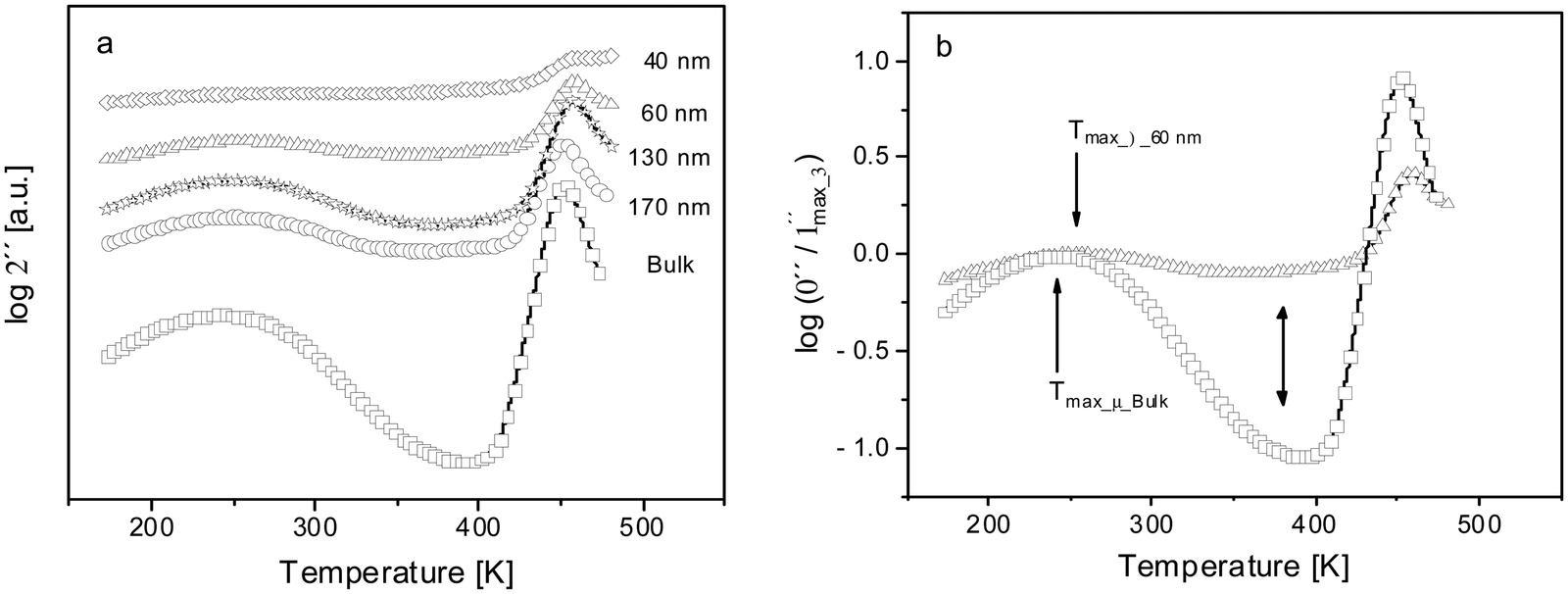 | ||
| Fig. 7 (a) Dielectric loss versus temperature at a fixed frequency of 105 Hz for the indicated film thicknesses: bulk PBAC – open squares, 170 nm – open circles, 130 nm – open stars, 60 nm – open triangles, and 40 nm – open diamonds. The spectra are shifted along the y-scale for sake of clearness. (b) Dielectric loss normalized by the maximum value of the β-relaxation versus temperature at a fixed frequency of 105 Hz. Bulk PBAC – open squares; 60 nm – open triangles. The single sided arrows indicate the temperature position of the peak height of the β-relaxation and the double-sided arrow shows the change in shape between the relaxation processes from bulk PBAC to 60 nm. | ||
Using a different approach, the dielectric loss was normalized by the maximal loss of the β-relaxation for both a bulk sample and a thin film with a thickness of 60 nm. The logarithm of this normalized dielectric loss is plotted versus temperature at a frequency of 105 Hz, depicted in Fig. 7(b). For the bulk sample, the β- and α-relaxation processes are well separated by a pronounced minimum. There is an agreement in the literature that the width of a β-relaxation process is due to a distribution of activation energies. Upon closer inspection of the dielectric loss in the temperature region of the β-relaxation for the thin films revealed that the peak of the β-process broadens with decreasing film thickness at its low and high temperature side. On the one hand, a broadening at the low temperature side means that there is an enhanced molecular mobility compared to the bulk. This could be understood by the high roughness of the Al electrodes (see above). This roughness will create some additional free volume sites which will ease some relaxation modes of the β-relaxation. On the other hand, a broadening on the high temperature side would mean that the molecular fluctuations responsible for the β-relaxation become more and more restricted with decreasing film thickness and appear at higher temperatures. This most likely indicates that the restriction takes place in the vicinity of the Al substrates and will percolate more and more through the film as the thickness of the bulk-like layer decreases with decreasing film thickness. Therefore, the gap between the β- and the α-relaxation is filled up by relaxation modes contributing in the bulk to the β-process. This is evidenced by the high dielectric loss between the β- and the α-relaxation. As the film thickness is decreased to thicknesses below 60 nm, the β-relaxation is no longer detected as an isolated pronounced peak as all the relaxation modes responsible for the β-relaxation are restricted and appear now in the temperature range between the β- and the α-relaxation. This interpretation is supported by the observation that the maximum temperature of the β-relaxation is shifted by ca. 12 K to higher temperatures compared to the bulk (see Fig. 7(b)). It is worth noting again that the thickness of 60 nm corresponded to the onset thickness where the strong increase of Tg with decreasing film thickness takes place.
For the thin films where the β-relaxation is observed as a separate peak down to a thickness of 60 nm. Unfortunately, the fitting of two HN-function to the spectra of the thin films leads to unstable results. Therefore, no separation into processes due to the π-flips and the 90° rotational fluctuations of the phenyl rings could be made. As a result, only one HN function and only the process at higher temperatures, the π–π – flips, could be analyzed and the estimated activation energies were between 37–40 kJ mol−1 (see Fig. 6). Nevertheless, the estimated activation energies have to be considered as a kind of averaged one of the two processes.
From the investigation of the growth kinetics of the adsorbed layer of PBAC on silicon oxide it was found that the thickness of the adsorbed layer should be ca. 5 nm for the annealing conditions employed here.37 As the film is capped between two Al electrodes the whole thickness of the adsorbed layer is ca. 10 nm. As the β-relaxation seems to disappear as a separate peak for film thicknesses below 60 nm, this points to a relative strong influence of the adsorbed layer on the bulk like layer regarding the molecular fluctuations of this process. From a quantitative analysis of the dielectric strength of α-relaxation a thickness of the adsorbed layer of 8 nm was concluded in ref. 43. As the samples discussed in ref. 43 were prepared by a different annealing procedure (24 h at Tg,Bulk + 17 K; here 72 h at Tg,Bulk + 30 K) it was expected that the thickness of the formed adsorbed layer is lower. This again points to the influence of the adsorbed layer on the bulk-like layer.
For the thin films measured in CEC geometry a further relaxation process was found at temperatures close to that of the α-relaxation for the thin films with a moderate thickness, see inset Fig. 8. This process, called the slow Arrhenius process (SAP), was previously investigated by Song et al.64 and Caporaletti et al.65 using dielectric spectroscopy for a variety of polymers including PBAC. The SAP was discussed as a molecular process related to the equilibration of polymers at temperatures lower than the glass transition.64 It is worth noting that the SAP process is important to understand physical aging in polymers deep in the glassy state which requires a process that is faster than the α-relaxation.64,66Fig. 7 shows the relaxation map for the SAP process in comparison to the α-relaxation for two samples with two different film thicknesses of 130 and 60 nm. The activation energy for the SAP of both film is approximately 72 kJ mol−1 and independent of film thickness. However, due to the result that the SAP is observed at lower frequencies compared to the α-relaxation, the dielectric loss can be masked by parasitic contributions like conductivity or polarization effects which become more relevant for thinner films. Consequently, the SAP could not be reliably found for film thicknesses below 48 nm in the CEC configuration. Compared to a previous study of the SAP for PBAC,64 the relaxation rates were shifted to slightly higher values, but in general agree with the results given here (see ESI,† Fig. S2).
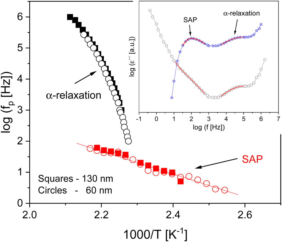 | ||
| Fig. 8 Relaxation map for films with thicknesses of 130 nm (squares) and 60 nm (circles) thin films for the α-relaxation and the SAP processes. The solid red line is an Arrhenius fit to the data. The inset depicts the dielectric loss versus frequency for a thin film with thickness of 60 nm at 457 K. The black circles represent the original data, and the blue stars are with the conductivity contribution subtracted. The SAP and the α-relaxation are highlighted in red. | ||
Nanostructured electrodes
Using the nanostructured electrodes configuration, the effect of the adsorbed layer can be investigated due to possibility of measuring thin films with thicknesses below 40 nm. As the thin films have a free surface at the polymer–air interface, this configuration may also allow an investigation into the effect of the mobile surface layer on the dielectric properties. Like for the thin films measured in CEC geometry, the structure of polymer chain is also highly asymmetric for the thin films measured by NSE. This is especially true for the film with a thickness of 14 nm and the adsorbed layer. Fig. 9 compares the dielectric loss versus temperature at a frequency of 103 Hz for a film with a thickness of 40 nm measured with CEC and NSE as well as for a bulk PBAC sample. The dielectric spectra for the sample measured using NSE shows both the β- and α-relaxation peaks at low and high temperatures, respectively. Due to the increased mobility of the segments at the free surface compared to a 40 nm sample measured with CEC, the β-relaxation is now observed and can be compared to bulk PBAC. Moreover, the maximum temperature position of the α-relaxation measured by NSE is shifted to lower temperature values compared to CEC and agrees approximately with that of bulk PBAC. This again can be discussed to the increased mobility as opposed to a capped geometry due to the free surface. | ||
| Fig. 9 Comparison of dielectric loss versus temperature for two films with a thickness of 40 nm measured with CEC (red stars) and NSE (green circles) as well as for bulk PBAC at a frequency f = 103 Hz. Lines are guides for the eyes. The spectra are shifted along the y-axis for sake of clarity. The α- and β-relaxation peaks are labelled. | ||
A comparison of the dielectric spectra measured using NSE for different film thicknesses, given in Fig. 10, reveals that the β-relaxation also broadens with a reduction in film thickness and disappears as a separated peak, similar to the behavior of the samples measured with CEC. The broadening and thereby reduction in intensity of the β-relaxation is due to the increasing contribution of the adsorbed layer to the dielectric loss of the whole film which restricts the fluctuations responsible for this process. Since silica spacers were used in the NSE geometry, no polymer–metal complexes are formed as was the case for CEC. Therefore, it can be assumed that the broadening and reduced intensity of the β-relaxation is due only to the physically adsorbed layer for the films measured in NSE geometry. For the 40 nm thin film measured using NSE, the activation energy for this localized process was 30.6 kJ mol−1. Although there are normally 2 coupled processes associated with the β-relaxation for PBAC, specifically phenylene ring rotations and π–π – flips. Here only one process can be analyzed like for the CEC arrangement. In Fig. S3, ESI,† the relaxation rates for the β-process are compared between bulk PBAC, a 170 nm thin film measured using CEC and a 40 nm sample measured with NSE. For the relaxation rate of the phenylene ring rotations, the sample measured with NSE is slower compared to bulk PBAC. This serves as further prove that the formation of the adsorbed layer restricts the fluctuations of the β-relaxation. It is important to point out that while the adsorbed layer has a profound effect on the β-relaxation, the presence of a free surface allows the β-relaxation to be visible and analyzed for the 40 nm thin film.
 | ||
| Fig. 10 The dielectric loss versus temperature at a frequency of 100 Hz for samples measured with the NSE configuration for the indicated film thickness: 40 nm – open squares, 26 nm – open circles, 18 nm – open triangles 14 nm – open diamonds and adsorbed layer (AL) – red open stars. The data is shifted along the y-axis for sake of clarity. The solid black line indicates the increase of the maximum temperature of the α-relaxation as the film thickness is reduced. For the film with a thickness of 14 nm and the adsorbed layer the dielectric loss could not be measured in the temperature range of the β-relaxation due to resonances caused nanostructured electrodes. | ||
The α-relaxation was observed in the dielectric loss down to a film thickness of 18 nm and shifts to higher temperatures as the film thickness is reduced. The α-relaxation could not be observed for a thin film with thickness 14 nm and the adsorbed layer sample. The HN function (eqn (5)) was fit to the dielectric loss data and the relaxation rate of the α-process was determined. The relaxation rates for the samples measured using NSE are compared with the thin film samples measured using CEC and bulk PBAC in a relaxation map depicted in Fig. 11.
 | ||
| Fig. 11 Relaxation map of the α-relaxation for thin films measured with CEC (solid symbols): 170 nm – red circles, 75 nm – green triangles, and 60 nm – purple diamonds and the thin films measured using NSE (open symbols): 40 nm – open squares, 26 nm – open circles, and 18 nm – open triangles. The α-relaxation for bulk PBAC – black squares was plotted alongside the data for the thin films. The red lines are VFT fits to data. | ||
The relaxation rates of the α-relaxation for the samples measured with NSE shift to higher temperatures with decreasing film thickness. This agrees with the behavior observed for the samples measured with CEC. For the 40 nm thin film measured using NSE, the temperature dependence of the relaxation rates of the α-relaxation is similar to that of a 75 nm thin film measured using CEC. This means that 40 nm is the thickness for supported thin films where below this value the glassy dynamics becomes influenced by the adsorbed layer. Above 40 nm, the molecular mobility of a supported film measured with NSE is expected to be comparable to a bulk sample although it could not be measured directly. In the CEC configuration, the onset thickness was 60 nm, which was due to the presence of two substrate interfaces compared to only one for the NSE configuration. Therefore, it can be concluded that both electrode configurations lead to a shift of the α-relaxation to higher temperature due to the presence of an adsorbed layer for both substrates.
The VFT equation (eqn (6)) was used to analyze the temperature dependence of the relaxation rates and the Vogel temperature was determined. Like for the fitting procedure of the CEC data the pre-factor f∞ was fixed to that of the bulk. Table S2 in the ESI† lists the fit parameters for the VFT equation for the thin films measured with NSE. In Fig. 12, the dependencies of the Vogel temperature on film thickness for thin films of PBAC are compared. Additionally, the thickness dependence of the glass transition temperature measured by ellipsometry is included in this figure. As discussed above the thickness dependence of T0 measured by CEC and Tg is comparable because of the comparable interaction energy between the substrates and PBAC. This is different for the dependence of T0 measured with the NSE configuration. Besides the lower onset thickness due to the free surface at polymer–air interface T0 increases much stronger with decreasing film thickness than that measured with the CEC arrangement. This difference can be discussed by the much higher interaction energy of PBAC with the employed doped silicon (3.56 mJ m−2) compared to that of Al (2.21 mJ m−2, see section interfacial energy). This higher interfacial will probably result in a denser adsorbed layer which has a more restricting influence on the glassy dynamics.
 | ||
| Fig. 12 Change in Vogel temperature T0 measured by BDS using CEC – black squares and NSE – black diamonds and the thermal glass transition temperature Tg – blue stars obtained from ellipsometry37versus film thickness. Lines are guides for the eyes for each data set. The inset compares the thickness dependence of the glass transition temperature estimated by ellipsometry (blue stars)37 with that measured by Torkelson et al.21 (black circles). The lines are guides for the eyes. | ||
In this work an increase in the Tg and T0 as the film thickness was reduced was found when measuring with both ellipsometry37 and dielectric spectroscopy. Yin et al.43 also reported an increase with reduced film thickness when measuring using the CEC configuration with BDS for PBAC. However, Torkelson et al.21 reported a decrease in the Tg with decreasing film thickness when measuring with fluorescence spectroscopy where the samples were prepared on Quartz glass (see inset Fig. 12). These differing film thickness dependencies can be explained by considering both the annealing conditions and the interfacial energies between the different substrates and PBAC. These two factors are vital for the growth of the adsorbed layer. The annealing conditions used by Torkelson et al.21 and Yin et al.43,53 were both weaker than that for the samples prepared in this investigation and in ref. 37. Therefore, the adsorbed layer formed was unable to compensate the confinement and free-surface effects. It is also worth noting that fluorescence-based measurements were found to overestimate the contribution of the free-surface layer when measuring thin films.67
The thin film with a thickness of 14 nm measured using NSE arrangement showed no α-relaxation (see Fig. 10). This means that the adsorbed layer restricted the segmental dynamics completely. In order to study the molecular dynamics of the adsorbed layer directly, an adsorbed layer sample was also investigated using NSE. The adsorbed layer sample was prepared by leaching a film which was spin coated on the bottom electrode with dichloromethane after annealing at T = 443 K for 72 h. For details see ref. 31. Using this technique only the tightly bounded layer remained on the bottom electrode and most of the segments were assumed to be adsorbed. At the interface of the adsorbed layer to air there may be segments which can be described as dangling ends. However, the structure of these dangling ends is different to the free surface layer of the thin films where the corresponding chains were not adsorbed to the most extent. Nevertheless, these dangling ends might introduce some additional molecular mobility to the adsorbed layer. The resulting thickness of the prepared adsorbed layer was 3.5 nm. As expected already from the behavior of the film with a thickness of 14 nm the spectrum of the adsorbed layer does not show a dynamic glass transition (see Fig. 10).
Unfortunately, the dielectric loss in the temperature range of the β-relaxation could not be measured for the 14 nm and the adsorbed layer sample due to resonances of the nanostructured electrode system. But it is expected for the spectra of the films with 26 and 18 nm measured by the NEC configuration that no β-relaxation could be observed.
Conclusion
The aim of this investigation was to extend a previous study into the molecular mobility of thin films of poly(bisphenol A carbonate). Thin films of poly(bisphenol A carbonate) were first measured between deposited aluminum layers in a capped geometry to investigate the molecular dynamics down to a film thickness of 40 nm. The glass transition characterized by the Vogel temperature increased with decreasing film thickness strongly for lower thickness than the onset thickness of 60 nm. The results obtained by dielectric spectroscopy agreed with data obtained by ellipsometry where the films were prepared under the same conditions. This similarity can be considered as proof that the contribution of the adsorbed layer had an increasing influence on the overall glassy dynamics of the thin films with decreasing film thickness. The β-relaxation consisted of two coupled processes due to localized fluctuations of the phenyl rings. With decreasing film thickness, a decrease in the intensity was reported as the corresponding relaxation shifts to higher temperatures. The β-relaxation could not be detected as a separate peak for thin film having thicknesses below 60 nm. This thickness additionally corresponded to the onset thickness where the Vogel temperatures started to increase strongly with decreasing film thickness. Moreover, a slow Arrhenius process was found for the thin film samples at temperatures near the α-relaxation and was assigned to the thin film equilibration kinetics.Nanostructured electrodes which had silica spacers with a height of 60 nm were used in conjunction with a SiO2 bottom electrode to study the molecular mobility of films below 40 nm and an adsorbed layer sample. This configuration allowed the polymer film to have a free surface with air due to the spacer height being larger than the film thickness. A β-relaxation was found for the 40 nm sample measured with NSE due to the free-surface allowing an increased mobility compared to the thin films measured with CEC. As the film thickness was reduced, the β-relaxation peak broadened due to the influence of the adsorbed layer and disappears as separate peak. An α-relaxation was observed in the dielectric loss down to a film thickness of 18 nm. It shifts to higher temperatures as the film thickness was reduced. Although the onset thickness was lower compared to the CEC configuration, the increase in T0 was much stronger for the NSE configuration. The stronger interfacial interactions between the silicon and PBAC resulted in a denser adsorbed layer which dominated the glassy dynamics as the film thickness was reduced. The results obtained here should be confirmed for other mainchain polymers like polysulfone.
Author contributions
HO prepared the samples, did the experiment, analyzed the data and wrote the first draft of the manuscript; SA helped with the sample preparation and the measurements; PS helped with analysis of the data and co-supervised the project. AS had the idea of the project, lead the and edit the final version of the manuscript. All authors agree with the publication.Data availability
The data are prat of an ongoing research project. Selected data will be available on reasonable request be the corresponding author.Conflicts of interest
There are no conflicts to declare.Acknowledgements
G. Hidde is thanked for the contact angle measurements. BAM is acknowledged for financial support in the frame of the PhD program.References
- Polymer Thin Films, ed. A. A. Hashim, In-Thech, Vukovar, Croatia, 2010, ISBN 978-953-307-059-9 Search PubMed.
- B. Li, S. Zhang, J. S. Andre and Z. Chen, Relaxation Behavior of Polymer Thin Films: Effects of Free Surfaces, Buried Interface, and Geometrical Confinement, Prog. Polym. Sci., 2021, 120, 101431 CrossRef CAS.
- X. Wu, X. Chen, Q. M. Zhang and D. Q. Tan, Advanced Dielectric Polymer for Energy Storage, Energy Storage Mater., 2022, 44, 29–47 CrossRef.
- J. L. Keddie, R. A. L. Jones and R. A. Cory, Size Dependent Depression of the Glass Transition Temperature in Polymer Films, EPL, 1994, 27(1), 59–64 CrossRef CAS.
- J. Forrest and K. Dalnoki-Veress, The Glass Transition in Thin Polymer Films, Adv. Colloid Interface Sci., 2001, 94(1–3), 167–195 CrossRef CAS.
- X. Zheng, M. H. Rafailovich, J. Sokolov, Y. Strzhemechny, S. A. Schwarz, B. B. Sauer and M. Rubinstein, Long-range Effects on Polymer Diffusion Induced by a Bounding Interface, Phys. Rev. Lett., 1997, 79(2), 241–244 CrossRef CAS.
- D. S. Fryer, R. D. Peters, E. J. Kim, E. Tomaszewski, J. J. de Pablo and P. F. Nealey, Dependence of the Glass Transition Temperature of Polymer Films on Interfacial Energy and Thickness, Macromolecules, 2001, 34(16), 5627–5634 CrossRef CAS.
- M. D. Ediger and J. A. Forrest, Dynamics Near Free Surfaces and the Glass Transition in Thin Polymer Films: a View to the Future, Macromolecules, 2014, 47(2), 471–478 CrossRef CAS.
- D. Labahn, R. Mix and A. Schönhals, Dielectric Relaxation of Ultrathin Films of Supported Polysulfone, Phys. Rev. E: Stat., Nonlinear, Soft Matter Phys., 2009, 79, 011801 CrossRef.
- S. Napolitano, A. Pilleri, P. Rolla and M. Wübbenhorst, Unusual Deviations from Bulk Behavior in Ultrathin Films of Poly(tert-butylstyrene): Can Dead Layers Induce a Reduction of Tg?, ACS Nano, 2010, 4(2), 841–848 CrossRef CAS.
- J. L. Keddie, R. A. L. Jones and R. A. Cory, Interface and Surface Effects on the Glass-Transition Temperature in Thin Polymer Films, Faraday Discuss., 1994, 98, 219–230 RSC.
- J. S. Sharp and J. A. Forrest, Free Surfaces Causes Reductions in the Glass Transition Temperature of Thin Polystyrene Films, Phys. Rev. Lett., 2003, 91(23), 235701 CrossRef CAS PubMed.
- S. Kawana and R. A. L. Jones, Character of the Glass Transition in Thin Supported Polymer Films, Phys. Rev. E, 2001, 63(2), 021501 CrossRef CAS PubMed.
- C. J. Ellison and J. M. Torkelson, Sensing the Glass Transition in Thin and Ultrathin Polymer Films via Fluorescence Probes and Labels, J. Polym. Sci., Part B: Polym. Phys., 2002, 40(24), 2745–2758 CrossRef CAS.
- V. M. Boucher, D. Cangialosi, H. Yin, A. Schönhals, A. Alegria and J. Colmenero, Tg Depression and Invariant Segmental Dynamics in Polystyrene Thin Films, Soft Matter, 2012, 8, 5119–5122 RSC.
- H. Huth, A. A. Minakov, A. Serghei, F. Kremer and C. Schick, Differential AC-Chip Calorimeter for Glass Transition Measurements in Ultra-Thin Polymeric Films, Eur. Phys. J.: Spec. Top., 2007, 141, 153–160 Search PubMed.
- A. Serghei and F. Kremer, Confinement-Induced Relaxation Process in Thin Films of Cis-Polyisoprene, Phys. Rev. Lett., 2003, 91(16–17), 165702 CrossRef CAS.
- A. Serghei, M. Tress and F. Kremer, The Glass Transition of Thin Polymer Films in Relation to the Interfacial Dynamics, J. Chem. Phys., 2009, 131, 154904 CrossRef CAS PubMed.
- K. Fukao and Y. Miyamoto, Glass Transitions and Dynamics in Thin Polymer Films: Dielectric Relaxation of Thin Films of Polystyrene, Phys. Rev. E: Stat., Nonlinear, Soft Matter Phys., 2000, 61, 1743–1754 CrossRef CAS PubMed.
- J. H. Kim, J. Jang and W.-C. Zin, Estimation of the thickness dependence of the glass transition temperature in various thin polymer films, Langmuir, 2000, 16, 4064–4067 CrossRef CAS.
- J. M. Torkelson, R. D. Priestley, P. Rittigstein, M. K. Mundra and C. B. Roth, Novel effects of confinement and interfaces on the glass transition temperature and physical aging in polymer films and nanocomposites, AIP Conf. Proc., 2008, 982, 192–195 CrossRef CAS.
- C. M. Evans, H. Deng, W. F. Jager and J. M. Torkelson, Fragility is a key parameter in determining the magnitude of Tg-confinement effects in polymer films, Macromolecules, 2013, 46, 6091–6103 CrossRef CAS.
- Z. Ma, H. Nie, J. Yan and O. K. C. Tsui, Correlation between fragility and surface glass transition temperature of polymers, J. Chem. Phys., 2023, 159, 224905 CrossRef CAS.
- H. Omar, S. Ahmadi, D. Hülagü, G. Hiddle, A. Hertwig, P. Szymoniak and A. Schönhals, Investigations of the adsorbed layer of polysulfone: influence of the thickness of the adsorbed layer on the glass transition of thin films, J. Chem. Phys., 2024, 161, 054904 CrossRef CAS.
- S. Napolitano and M. Wübbenhorst, The Lifetime of Deviations from Bulk Behaviour in Polymers Confined at the Nanoscale, Nat. Commun., 2011, 2(260), 1–7 Search PubMed.
- C. Rotella, S. Napolitano, S. Vandendriessche, V. K. Valev, T. Verbiest, M. Larkowska, S. Kucharski and M. Wübbenhorst, Langmuir, 2011, 27(22), 13533–13538 CrossRef CAS.
- S. Granick, Perspective: Kinetics and Mechanical Properties of Adsorbed Polymer Layers, Eur. Phys. J. E: Soft Matter Biol. Phys., 2002, 9, 421–424 CrossRef CAS.
- C. Rotella, S. Napolitano, L. De Cremer, G. Koeckelberghs and M. Wübbenhorst, Macromolecules, 2010, 43(20), 8686–8691 CrossRef CAS.
- H. Mortazavian, C. Fennell and F. Blum, Structure of the Interfacial Region in Adsorbed Poly(Vinyl Acetate) on Silica, Macromolecules, 2016, 49(11), 4211–4219 CrossRef CAS.
- O. Guiselin, Irreversible Adsorption of a Concentrated Polymer Solution, Europhys. Lett., 1992, 17(3), 225–230 CrossRef CAS.
- C. Housmans, M. Sferrazza and S. Napolitano, Kinetics of Irreversible Chain Adsorption, Macromolecules, 2014, 47(10), 3390–3393 CrossRef CAS.
- M. Sen, N. Jiang, J. Cheung, M. K. Endoh, T. Koga, D. Kawaguchi and K. Tanaka, Flattening Process of Polymer Chains Irreversibly Adsorbed on a Solid, ACS Macro Lett., 2016, 5(4), 504–508 CrossRef CAS PubMed.
- M. Gawek, H. Omar, P. Szymoniak and A. Schönhals, Growth kinetics of the adsorbed layer of poly(2-vinyl pyridine) – an indirect observation of desorption of polymers from substrates, Soft Matter, 2023, 19(21), 3975–3982 RSC.
- N. Jiang, J. Shang, X. Di, M. K. Endoh and T. Koga, Formation mechanism of high-density flattened polymer nanolayers adsorbed on planar solids, Macromolecules, 2014, 47(8), 2682–2689 CrossRef CAS.
- M. F. Thees, J. A. McGuire and C. B. Roth, Review and Reproducibility of Forming Adsorbed Layers from Solvent Washing of Melt Annealed Films, Soft Matter, 2020, 16(23), 5366–5387 RSC.
- S. Napolitano, Irreversible adsorption of polymer melts and nanoconfinement effects, Soft Matter, 2020, 16, 5348–5365 RSC.
- H. Omar, G. Hiddle, P. Szymoniak, A. Hertwig and A. Schönhals, Growth kinetics of the adsorbed layer of poly(bisphenol A carbonate) and its effect on the glass transition behavior in thin films, RSC Adv., 2023, 13(21), 14473–14483 RSC.
- K. Fukao and Y. Miyamoto, Glass transition and dynamics in thin polymer films: dielectric relaxation of thin films of polystyrene, Phys. Rev. E: Stat., Nonlinear, Soft Matter Phys., 2000, 61, 1743 CrossRef CAS.
- M. Tress, M. Erber, E. U. Mapese, H. Huth, J. Müller, A. Serghei, C. Schick, K.-J. Eichhorn, B. Voit and F. Kremer, Glassy dynamics and glass transition in nanometric thin layers of polystyrene, Macromolecules, 2010, 43(23), 9937–9944 CrossRef CAS.
- H. Yin, D. Cangialosi and A. Schönhals, Glass transition and segmental dynamics in thin supported polystyrene films: the role of molecular weight and annealing, Thermochim. Acta, 2013, 566, 186–192 CrossRef CAS.
- K. Fukao, Dynamics in Thin Polymer Films by Dielectric Spectroscopy, Eur. Phys. J. E: Soft Matter Biol. Phys., 2003, 12, 119–125 CrossRef CAS.
- R. Winkler, U. A. B. Unni, W. Tu, K. Chat and K. Adrjanowicz, On the segmental dynamics and the glass transition behavior of poly(2-vinylpyridine) in one and two dimensional nanometric confinement, J. Phys. Chem. B, 2021, 125, 5991–6003 CrossRef CAS.
- H. Yin, S. Napolitano and A. Schönhals, Molecular Mobility and Glass Transition of Thin Films of Poly(bisphenol A carbonate), Macromolecules, 2012, 45(3), 1652–1662 CrossRef CAS.
- M. Tress, E. U. Mapesa, W. Kossack, W. K. Kipnusu, M. Recihe and F. Kremer, Glassy Dynamics in Condensed Isolated Polymer chains, Science, 2013, 341(6152), 1371–1374 CrossRef CAS PubMed.
- S. Madkour, P. Szymoniak, M. Heidari, R. von Klitzing and A. Schönhals, Unveiling the Dynamics of Self-Assembled Layers of Thin Films of Poly(vinyl methyl ether) (PVME) by Nanosized Relaxation Spectroscopy, ACS Appl. Mater. Interfaces, 2017, 9(8), 7535–7546 CrossRef CAS PubMed.
- S. Dimitrellou, D. Iakovidis and D.-R. Psarianos, Mechanical characterization of polylactic acid, polycarbonate, and corbon fiber reinforced polyamide specuments fabricated by fused deposition modeling, J. Mater. Eng. Perform., 2024, 33, 3613–3626 CrossRef CAS.
- https://gwyddion.net/ .
- T. Strunskus, V. Zaporojtchenko, K. Behnke, C. v. Bechtolsheim and F. Faupel, Tailoring the Morphology of Metal/Polymer Interfaces, Adv. Eng. Mater., 2000, 2, 489–492 CrossRef.
- L.-H. Lee, Correlation between Lewis acid−base surface interaction components and linear solvation energy relationship solvatochromic α and β parameters, Langmuir, 1996, 12, 1681–1687 CrossRef CAS.
- D. K. Owens and R. C. Wendt, Estimation of the surface free energy of polymers, J. Appl. Polym. Sci., 1969, 13, 1741–1747 CrossRef CAS.
- D. H. Kaelble, Dispersion-polar surface tension properties of organic solid, J. Adhes., 1970, 2, 66–81 CrossRef CAS.
- R. J. Good and L. A. Girifalco, A theory for estimation of surface and interfacial energies III. Estimation of Surface Energies of Solids from Contact Angle Data, J. Phys. Chem., 1960, 64, 561–565 CrossRef CAS.
- H. Yin and A. Schönhals, Calorimetric glass transition of ultrathin poly(bisphenol A carbonate) films, Soft Matter, 2012, 8, 9132–9139 RSC.
- A. Schönhals and F. Kremer, Analysis of Dielectric Spectra, in Broadband Dielectric Spectroscopy, ed. F. Kremer and A. Schönhals, Springer, Berlin, Heidelberg, 2003 Search PubMed.
- S. Havriliak and S. Negami, A complex plane analysis of α-dispersions in some polymer systems, J. Polym. Sci., Part C, 1966, 14(1), 99–117 CrossRef.
- S. Madkour, P. Szymoniak, J. Radnik and A. Schönhals, Unraveling the Dynamics of Nanoscopically Confined PVME in Thin Films of a Miscible PVME/PS Blend, ACS Appl. Mater. Interfaces, 2017, 9, 37289–37299 CrossRef CAS.
- H. D. Vogel, Temperaturabhangigkeitsgesetz der Viskosität von Flüssigkeiten, Phys. Z, 1921, 22, 645–646 CAS.
- G. S. Fulcher, Analysis of Recent Measurements of the Viscosity of Glasses, J. Am. Ceram. Soc., 1925, 8, 339–355 CrossRef CAS.
- G. Tammann and W. Hesse, Die Abhängigkeit der Viskosität von der Temperatur bei unterkühlten Flüssigkeiten, Z. Anorg. Allg. Chem., 1926, 156, 245–257 CrossRef CAS.
- C. A. Angell, Relaxation in liquids, polymers and plastic crystals—strong/fragile patterns and problems, J. Non-Cryst. Solids, 1991, 131–133, 13–31 CrossRef CAS.
- A. Alegria, O. Mitxelena and J. Colmenero, On the Molecular Motions Originating from the Dielectric γ-Relaxation of Bisphenol-A Polycarbonate, Macromolecules, 2006, 39(7), 2691–2699 CrossRef CAS.
- S. Arrese-Igor, O. Mitxelena, A. Arbe, A. Alegria, J. Colmenero and B. Frick, Effect of Stretching on the Sub-Tg Phenylene-Ring Dynamics of Polcarbonate by Neutron Scattering, Phys. Rev. E: Stat., Nonlinear, Soft Matter Phys., 2008, 78(2), 021801 CrossRef.
- C. Massoro, Q. T. Le and J. Pireaux, XPS/AFM study of thermally evaporated aluminum/polycarbonate interface, J. Surf. Interface Anal., 1994, 21, 425–429 CrossRef.
- Z. Song, C. Rodriguez-Tinoco, A. Mathew and S. Napolitano, Fast Equilibration Mechanisms in Disordered Materials Mediated by Slow Liquid Dynamics, Sci. Adv., 2022, 8(15), 1–7 Search PubMed.
- F. Caporaletti and S. Napolitano, The Slow Arrhenius Process in Small Organic Molecules, Phys. Chem. Chem. Phys., 2024, 26, 745 RSC.
- D. Cangialosi, Physical aging and vitrification in polymers and other glasses: Complex behavior and size effects, J. Polym. Sci., 2024, 62, 1952–1974 CrossRef CAS.
- S. Kim, S. A. Hewlett, C. B. Roth and J. M. Torkelson, Confinement effects on glass transition temperature, transition breadth, and expansivity: Comparison of ellipsometry and fluorescence measurements on polystyrene films, Eur. Phys. J. E: Soft Matter Biol. Phys., 2009, 30, 83–92 CrossRef CAS PubMed.
Footnote |
| † Electronic supplementary information (ESI) available: Derivative analysis for film with thicknesses of 60 nm and 45 nm; relaxation map for the SAP, values of the measured contact angels; relaxation map of the β-relaxation, VFT parameters. See DOI: https://doi.org/10.1039/d4sm01238k |
| This journal is © The Royal Society of Chemistry 2025 |