
 Open Access Article
 This Open Access Article is licensed under a Creative Commons Attribution-Non Commercial 3.0 Unported Licence
A novel particulate photocathode composed of CdTe–ZnTe solid solutions with a composition gradient for solar hydrogen evolution from water†
Lionel S.
Veiga
 ab,
Mamiko
Nakabayashi
c,
Takenori
Fujii
d,
Masakazu
Sugiyama
ab and
Tsutomu
Minegishi
*ab
ab,
Mamiko
Nakabayashi
c,
Takenori
Fujii
d,
Masakazu
Sugiyama
ab and
Tsutomu
Minegishi
*ab
aResearch Center for Advanced Science and Technology (RCAST), Japan. E-mail: tmine@enesys.rcast.u-tokyo.ac.jp
bThe University of Tokyo, 4-6-1, Komaba, Meguro-ku, Tokyo, Japan
cInstitute of Engineering Innovation, School of Engineering, The University of Tokyo, 2-11-16, Yayoi, Bunkyo-ku, Tokyo, 113-8656, Japan
dCryogenic Research Center, The University of Tokyo, 2-11-16, Yayoi, Bunkyo-ku, Tokyo, 113-8656, Japan
First published on 17th June 2025
Abstract
Particulate photoelectrodes are promising for the development of innovative unbiased water-splitting devices by combining a photoanode and a photocathode. This configuration relaxes the requirements for band edge potentials of oxygen- and hydrogen-evolution systems while enhancing the solar-to-hydrogen conversion efficiency. However, particulate photocathodes often exhibit lower performance than thin-film-based photocathodes because of the difficulty of implementing functional structures. In this study, a novel CdTe-based particulate photocathode prepared via the modified particle transfer method, along with a ZnTe contact layer introduced via the close-spaced sublimation method, is presented. A ZnxCd1−xTe (0 ≤ x ≤ 1) solid solution with a composition gradient is produced under appropriate preparation conditions, and the conduction-band minimum gradient introduced by the composition gradient suppresses charge recombination and shifts the onset potential of the cathodic photocurrent to +0.7 VRHE. The introduction of a Cu layer to the back contact and post-deposition rapid thermal annealing further enhances the photocurrent, which reaches −7 mA cm−2 at 0 VRHE and a half-cell solar-to-hydrogen efficiency of 1.1% at 0.28 VRHE. The photocathode also exhibits an incident photon-to-current conversion efficiency (IPCE) of 36% at 520 nm and greater than 10% IPCE across the wavelength range 440–800 nm, which is the highest IPCE reported thus far for a particulate photocathode. These findings demonstrate the potential of the method of introducing a composition gradient for enhancing photoelectrochemical and photocatalytic hydrogen evolution.
Introduction
The environmental urgency surrounding greenhouse gas emissions from the utilization of fossil resources highlights the urgent need for a transition toward a carbon-neutral society. Fossil fuels are used not only for energy generation but also to produce essential chemicals such as ammonia, which is mainly used for the production of agricultural fertilizers.1 Photocatalytic or photoelectrochemical (PEC) water splitting offers a promising pathway to produce CO2-free H2 directly from solar energy. For efficient H2 production from water using sunlight, the utilization of a wide wavelength range that includes visible–infrared light is indispensable, indicating that narrow-bandgap materials are required in addition to suitable band edge potentials for the water-splitting reaction (i.e., a valence-band maximum (VBM) deeper than the redox potential of O2/H2O and a conduction-band minimum (CBM) shallower than the redox potential of H+/H2).29–31 However, because of their narrow bandgap, visible–infrared-light-responsive materials cannot easily fulfill the requirements for band edge potentials. n-Type and p-type semiconductors act as photocathodes and photoanodes, respectively. When such photocathodes and photoanodes are combined, the resultant photoelectrodes can relax the requirements for band edge potentials because their driving forces for the reaction are summed.2,32One of the advantages of PEC water splitting is that particulate materials can be used because of the flexibility of solid–liquid interfaces. Particulate-material-based PEC devices offer a promising pathway for scalable and innovative designs in integrated solar-to-hydrogen conversion devices such as photocatalyst sheets, particulate electrodes, and membrane photoelectrode assemblies.3–6 However, thin-film- and/or single-crystalline-wafer-based devices typically show superior performance over particulate-material-based PEC devices. The reasons for the superior properties of PEC devices based on thin films and/or single-crystalline wafers are the applicability of layered structures and/or a smaller number of defects. In particular, thin-film-based photoelectrodes can be fabricated with well-designed layered structures, enabling the band alignment to be optimized for the separation of photoexcited carriers.7
Most semiconductors cannot alone drive the hydrogen evolution reaction (HER) efficiently because of two primary limitations: rapid recombination of photogenerated electrons and holes before they reach the reaction sites and the inherent slowness of the surface reaction itself, which increases the likelihood of charge recombination. To address these challenges, researchers have developed layered structures as an effective strategy for enhancing photocathode performance. Sequential surface modifications with a thin n-type semiconductor layer and HER catalysts substantially accelerate the HER by enhancing both charge separation and surface reactions.8 HER enhancement by the aforementioned sequential surface modification has been reported for polycrystalline thin-film systems such as Cu(In,Ga)Se2, Cu2ZnSnS4, (Zn,Cd)Te, and (ZnSe)0.85(Cu(In0.7,Ga0.3)Se2)0.15.9–15 This strategy is also applicable to photocatalytic-particle-based photocathodes. For example, Goto et al. applied sequential surface modifications to a particulate (ZnSe)0.85(CuIn0.7Ga0.3Se2)0.15 solid solution ((ZnSe)0.85(CIGS)0.15)-based photocathode fabricated using particle transfer.16 The particulate (ZnSe)0.85(CIGS)0.15-based photocathode with a Mo contact layer and Ti conductor layer surface modified with Pt (Ti/Mo/(ZnSe)0.85(CIGS)0.15/Pt) exhibited a limited photocurrent of −0.5 mA cm−2 at 0 VRHE, with an onset potential (OP) of 0.7 VRHE under AM 1.5G simulated sunlight. However, a Ti/Mo/(ZnSe)0.85(CIGS)0.15 photocathode surface sequentially modified with cadmium sulfide (CdS), zinc sulfide (ZnS), and Pt (Ti/Mo/(ZnSe)0.85(CIGS)0.15/CdS/ZnS/Pt) yielded an exceptional photocurrent of −4.3 mA cm−2 at 0 VRHE with a notably high OP of 0.8 VRHE and half-cell solar-to-hydrogen conversion (HC-STH) efficiency of 0.83% at 0.33 VRHE. The authors attributed the observed increase in the cathodic photocurrent and OP resulting from the introduction of CdS and ZnS layers to appropriate band alignment and a thickened depletion layer at the solid–liquid interface. Both CdS and ZnS are n-type semiconductors, and surface modification of a photocathode with a thin n-type semiconductor layer leads to thickening of the depletion layer through modulation of the built-in potential. The thicker depletion layer is beneficial for charge separation. In addition, the considerably deep VBM of ZnS and CdS prevents surface recombination because the formed VBM offset acts as a barrier for holes, which are the majority carriers in (ZnSe)0.85(CIGS)0.15. Furthermore, Pt plays a crucial role as a cocatalyst by accelerating the reaction kinetics of photogenerated electrons with H+ ions by providing active surface sites that facilitate reduction reactions. Beyond the aforementioned strategies, introducing Na2S during the solid-state reaction, which increased crystal quality, was found to further improve the efficiency of the (ZnSe)0.85(CIGS)0.15 photocathode. The photocathode demonstrated a notable HC-STH efficiency of 1.1% at 0.37 VRHE, which is currently the highest reported value for a particulate photocathode. However, the device performance remains limited by a low incident-photon-to-current conversion efficiency (IPCE) of 25% at wavelengths shorter than 560 nm.
Although layered structures improve the HER efficiency in particulate photocathodes, further improving the performance requires strategies for harnessing photoexcited carriers near the flat-band potential. When a semiconductor is immersed in water, the electrolyte becomes the majority carrier and a depletion layer is formed. The band bending resulting from formation of the depletion layer is the primary driver of charge separation, and the height of the barrier formed by the band bending is equal to the difference between the potential, the Fermi level, and the flat-band potential of the photoelectrode. In the region near the flat-band potential, the depletion layer becomes thinner, substantially reducing the driving force for charge separation. Introducing a composition gradient has shown promise for enhancing the PEC properties of photocathodes.17 For instance, a (ZnSe)0.85(CIGS)0.15 thin-film photocathode prepared with a bilayer structure composed of a defined In-rich layer and a Ga-rich layer demonstrated a HC-STH efficiency of 3.6% with an IPCE maximum of >60%. Building on this approach, our group developed (ZnSe)0.85(CIGS)0.15 thin films with a continuous composition gradient between the In-rich and Ga-rich regions, producing a CBM gradient that facilitates the collection of photoexcited electrons generated outside the depletion layer to the HER sites. Consequently, the composition-graded (ZnSe)0.85(CIGS)0.15 thin film achieved an HC-STH efficiency of 4.5% and a maximum IPCE of 89%. The CBM gradient is expected to be particularly effective for enhancing the cathodic photocurrent at potentials near the OP, where the thinner depletion layer formed at the semiconductor–electrolyte interface results in weaker charge separation. However, the expected increase in the photocurrent at approximately the OP was not observed clearly because of the composition change resulting from the preparation conditions used to form a composition gradient.
II–IV semiconductor compounds, such as cadmium telluride (CdTe) and zinc telluride (ZnTe), are promising candidates for use in photocathodes because they are simple binary compounds composed of inexpensive elements, making them realistic materials for large-scale industrial production. CdTe, with its narrow bandgap of 1.5 eV, offers an absorption edge wavelength of 830 nm, a high absorption coefficient of >104 cm−1 at wavelengths shorter than 800 nm, and an expected photocurrent density of 29 mA cm−2 under standard AM 1.5G sunlight.18,19 ZnTe has been widely used as a hole-selective back contact layer in CdTe-based photovoltaic devices.20 With a large bandgap of 2.2 eV and a VBM closely aligned with that of CdTe, ZnTe enables the formation of a CBM offset, promoting hole-selective charge carrier diffusion to the backside electrode and suppressing recombination.21 In addition, CdTe and ZnTe both have the zinc blende crystal structure, enabling the formation of ZnxCd1−xTe (0 < x < 1) solid solutions and, thus, tuning of the bandgap and CBM potential through changes in the composition ratio.22
Recently, a ZnxCd1−xTe (0 < x < 1)-based photocathode with a relatively high OP, >0.7 VRHE and a photocurrent approximately equal to the OP (−4.0 mA cm−2 at 0.5 VRHE) has been reported.23 A ZnxCd1−xTe (0 < x < 1)-based photocathode was prepared by the Cu-mediated interdiffusion method, where ZnTe and CdTe layers were sequentially deposited via the close space sublimation (CSS) method and the presence of Cu enhanced interdiffusion between the ZnTe and CdTe layers. As a result, the melting point of ZnxCd1−xTe (0 < x < 1) was lowered, enabling interdiffusion and the formation of a ZnxCd1−xTe (0 < x < 1) layer with a composition gradient. Interestingly, the addition of Cu enhances the formation of thick and monocrystalline columnar grains, which are a preferable structure, and decreases the series resistance. The composition gradient introduced into the advantageously structured photocathode enhances charge separation and enables the utilization of electrons photoexcited outside of the depletion layer. The photocathodes with a composition gradient exhibited a high photocurrent density of −15.1 mA cm−2 at 0 VRHE and −4.0 mA cm−2 at 0.5 VRHE, which is the highest value reported for a CdTe- and ZnTe-based photocathode, with an OP exceeding 0.7 VRHE.23 We concluded that band engineering strategies such as the use of a band offset in the backside contact and/or a composition gradient are effective for suppressing the recombination of photoexcited carriers in photoelectrodes. However, the application of the strategy to particulate PEC devices has been limited. Asakura et al. reported that introducing a band offset in the back contact enhances the photocurrent by suppressing charge recombination at the backside electrode.24 To the best of our knowledge, the literature contains no reports of a composition gradient being introduced into particulate photoelectrodes.
In the present study, we constructed a powder-based photocathode using photocatalytic materials with an absorption edge in the near-infrared region. We first created a compositional gradient structure in photocatalytic particles, which substantially promoted PEC hydrogen production. To achieve the novel structure, we developed a modified particle transfer (MPT) method that involves forming a composition gradient structure through thermal diffusion. The aim of this work was to design guidelines for photoelectrodes beyond the appropriate control of solid–liquid interfaces based on physical chemistry. The particle transfer method was used to fabricate CdTe particle-based photocathodes.25 Conducting and semiconducting materials have been used to form preferred back contacts, typically ohmic contacts. However, the back contact can provide recombination sites because of the lack of hole/electron selectivity. To overcome this issue, we used ZnTe as the contact-layer material and formed a hole-selective back contact with CdTe.
Another major disadvantage of particulate systems compared with thin-film systems used as photoelectrodes is the difficulty in using a layered structure that can facilitate charge separation. In addition to modifying the surface with CdS and Pt, we successfully introduced a composition gradient structure into the particulate photocathode through interdiffusion between CdTe particles and the ZnTe back contact and the formation of ZnxCd1−xTe (0 < x < 1). The functional structure introduced into the photocatalytic particles enabled us to efficiently use photoexcited electrons outside the depletion layer, in addition to their photoexcitation and efficient use within the depletion layer. A particulate CdTe-based photocathode with a ZnTe back contact layer and Au conductor layer was successfully fabricated via the CSS method for the ZnTe layer and the vacuum evaporation method for the Au layer. Structural analysis revealed the epitaxial deposition of an approximately 4 μm-thick ZnTe film over the CdTe particles by the CSS method. The insertion of a ZnTe back contact layer between the particulate CdTe and the Au conductor layer led to a reduced series resistance with a sixfold increase in photocurrent to 4.14 mA cm−2 at 0 VRHE and a positive OP shift of +0.22 VRHE, which we attributed to the formation of a ZnxCd1−xTe solid solution with a composition gradient at the particle–film interface. Further enhancement was achieved by addition of Cu after ZnTe deposition, followed by rapid thermal annealing (RTA), resulting in one of the highest HC-STH efficiencies of 1.1% at 0 VRHE and an OP of 0.7 VRHE. The IPCE spectrum revealed a maximum value of 36% at 520 nm, with values exceeding 10% over a broad wavelength range from 440 to 800 nm, representing the highest level IPCE values reported thus far for a particulate photocathode.
Experimental
Preparation of CdTe particles
Micrometric and submicrometric CdTe particles were obtained through a two-step process. In the first step, commercial CdTe particles (Thermo Fisher Scientific, 99.9999% purity) were softly ground with an alumina ceramic mortar until a homogeneous powder was formed. The obtained particulate CdTe was then subjected to ball grinding with 10 mm-diameter zirconia balls for 1 h at 300 rpm in methanol. The ball-ground CdTe suspension was placed in a conical tube and subjected to centrifugal separation. Prior to the centrifugal separation, precipitates containing coarse particles were removed and then few-micron-sized CdTe particles were obtained by removing the supernatant via centrifugal separation at 1500 rpm for 1 min.Preparation of the photocathode by the MPT method
CdTe particles suspended in methanol were deposited onto 1 × 1 cm2 glass slides by drop casting. A ZnTe layer was deposited onto the particulate CdTe layer by the CSS method using particulate ZnTe (Kojundo, 99.99% purity) as an evaporation source. The ZnTe source temperature, substrate temperature (Tsubstrate), and deposition time were 850 °C, 300–475 °C, and 105–780 s, respectively. The substrate–source distance, Ar flow rate, and pressure in the CSS chamber were 10.5 cm, 50 sccm, and 6.0 Pa, respectively. During the CSS deposition of ZnTe, interdiffusion between CdTe particles and ZnTe occurred under appropriate deposition conditions, as discussed below. Following deposition of the ZnTe layer, a Cu layer with a thickness of 3–24 nm was deposited by physical vacuum evaporation (PVE). When the samples were annealed at 300 °C for 5 min under ambient N2 or vacuum conditions, Cu was introduced into the photocatalytic material via thermal diffusion. Notably, the doping by Cu substantially decreased the series resistance (Rs) of the photocathode.The photoelectrode fabrication scheme is summarized in Fig. S1 in the ESI.† A nominally 2.5 μm-thick Au layer was deposited onto the CdTe particles modified by deposition of the ZnTe and Cu layers through PVE. During deposition of the Au layer, the deposition rate of Au was adjusted to be 4 Å s−1, and the chamber pressure was maintained at 10−3 Pa. The assembly of Au foil and modified CdTe particles was picked up and fixed onto a glass slide using carbon tape as glue. The excess particles on the photocathode were removed by sonication in water for 3 min, and surface-modification treatments were applied. The photocathode surface was first surface modified with a CdS layer via chemical bath deposition (CBD) to promote charge separation at the solid–liquid interface, as previously reported.10 A chemical bath composed of a 50 mL aqueous solution of cadmium acetate (Fujifilm Wako Pure Chemical, 98.0%), thiourea (Fujifilm Wako Pure Chemical, 98.0%), and ammonia (Fujifilm Wako Pure Chemical) at concentrations of 25 mM, 375 mM, and 14 wt%, respectively, was used. The chemical bath solution in the beaker was first cooled to 10 °C, and the samples were soaked in this chemical bath. The beaker was then immediately soaked in a water bath with a temperature of 60 °C. After 14 min of CBD, the samples were picked up and sonicated in pure water for 1 min, followed by annealing in air at 200 °C for several minutes. Finally, as a HER catalyst, a nominally 2 nm-thick Pt layer was deposited onto the CdS-modified photocathodes via PVE using a 0.5 mm-thick Pt wire (Nilaco, 99.98%) as the evaporation source. Finally, the Cu wire was connected to the Au foil and the photocathode was encapsulated with an epoxy resin except for an active area. Table S3 in the ESI† shows a summary of sample labels and associated fabrication parameters.
Preparation of the tandem PEC device
The photoanode was prepared following the method reported by Kageshima et al.33 A commercially available Nb-doped SrTiO3 (Nb:STO) single-crystalline wafer was used as the front-side photoanode component in the tandem PEC cell. A tantalum (Ta) contact layer and an indium tin oxide (ITO) conductive layer were sequentially deposited on the back side of the Nb:STO wafer by radio frequency (RF) magnetron sputtering (ULVAC, MNS-2000RF) at a power of 30 W and a substrate temperature of 400 °C. Ta and ITO layers were deposited for 1 and 10 minutes, respectively. The Ta layer thickness was optimized to balance photocurrent generation with optical transmittance. Following deposition, the back-contact-modified wafer was bonded to an ITO-coated glass substrate using In and encapsulated with epoxy resin, leaving only the active area exposed for PEC measurements. Finally, the photoanode was positioned in front of the CdTe-based photocathode and electrically connected via a Cu wire to complete the tandem PEC device configuration as shown in Fig. S25 in the ESI.†Photoelectrochemical measurements
PEC measurements were conducted in a typical three-electrode setup using a potentiostat (Hokuto Denko HSV-110 and Princeton Applied Research VersaSTAT4). An Ag/AgCl electrode in saturated KCl and a Pt wire were used as the reference and counter electrodes, respectively. The measurements were performed using a gas-tight glass cell purged with Ar to avoid the O2 reduction reaction and to measure the amount of evolved H2. An aqueous phosphate electrolyte buffer solution (KPi) of 1 M KH2PO4, whose pH was adjusted to 6.5, was used as an electrolyte. A solar simulator (San-ei Electric XES-40S2) and a 300 W Xe lamp (Lamp House R300-3J) connected to a monochromator (Jasco CT-10) were used as light sources. The photon flux of monochromatic light was measured using a calibrated Si photodiode (Hamamatsu S2281-0). The gas product analysis was performed using a gas-tight cell equipped with a micro-gas chromatograph (microGC) (Agilent 490).Characterization
Morphological and compositional characterization studies were simultaneously performed using scanning electron microscopy (SEM; Thermo Scientific Phenom ProX) in conjunction with energy-dispersive X-ray spectroscopy (EDS). Electron backscatter diffraction (SEM-EBSD; JEOL JSM-7000F) mapping images were obtained from cross-section samples, which were prepared using an Ar-ion slicer (Cross-Section Polisher; JEOL SM-09010CP). The structural and optical properties were characterized by X-ray diffraction (XRD) using the Cu Kα line (Malvern Panalytical Aeris) and by UV–Vis diffuse-reflectance spectroscopy (UV–Vis DRS; Jasco V-670). The work function was measured using photoelectron spectroscopy in air (PESA; Riken Keiki AC-3).Results and discussion
Top- and cross-sectional-view SEM images of CdTe-based particulate photocathodes prepared by the MPT method are shown in Fig. 1 and 2, respectively. The surface of a photocathode prepared using particulate CdTe and a Au conductor layer (Au/CdTe) was densely coated with CdTe particles (Fig. 1A). Simultaneously acquired SEM-EDS mapping results (Fig. S2 in the ESI†) indicate slight exposure of the Au conductor layer between CdTe particles. The cross-sectional SEM-EDS observations (Fig. 2A and D) confirm the successful formation of a monoparticle layer on the Au foil. Top-view SEM-EDS analysis results for the particulate CdTe-based photocathode with an approximately 3 μm-thick ZnTe back contact layer and 2 μm Au conductor layer (Au/ZnTe/CdTe) (Fig. 1B and S3 in the ESI†) confirm that the partial exposure of Au was almost eliminated and that the ZnTe layer was substantially exposed under the optimized preparation conditions. The partially porous surface morphology of the CdTe layer indicates that the high deposition temperature led to partial evaporation of the CdTe particles during the CSS deposition of the ZnTe layer. The cross-sectional SEM-EDS analysis results for the Au/ZnTe/CdTe photocathode confirm the successful formation of monoparticle-layer Au foil with a ZnTe layer between the CdTe and Au layers. | ||
| Fig. 1 Plan-view SEM image of (A) Au/CdTe, (B) Au/ZnTe/CdTe, and (C) Au/Cu/ZnTe/CdTe (RTA). Scale bars: 10 μm. | ||
 | ||
| Fig. 2 Cross-sectional SEM images of (A) Au/CdTe, (B) Au/ZnTe/CdTe, and (C) Au/Cu/ZnTe/CdTe (RTA) and the corresponding SEM-EDS mappings (D–F, respectively). SEM-EDS line analysis results of the cross-sectional images in (A–C) are indicated by dashed lines. Scale bars: 4 μm. | ||
The top and cross-sectional SEM-EDS analysis results for the CdTe-based photocathode with a ZnTe back contact, 6 nm Cu addition, 2 μm Au foil, and post RTA treatment at 300 °C for 5 min (Au/Cu/ZnTe/CdTe (RTA)) are similar to those for Au/ZnTe/CdTe (Fig. 1C, 2C and D). The SEM-EDS line-scan analysis results (Fig. 2G) reveal that both Au/ZnTe/CdTe and Au/Cu/ZnTe/CdTe (RTA) showed similar variations in the Zn/(Zn + Cd) atomic composition ratio in the depth direction. The Zn/(Zn + Cd) ratio increased toward the backside of the photocathode, and the composition gradient region covered the entire CSS-deposited part and some of the particle part. Notably, a few microns of CdTe particles survived as-is. We concluded that the Cu addition and post RTA treatment did not affect the photocathode structure.
High-resolution cross-sectional SEM backscattered electron images and SEM-EBSD mapping images were acquired for the Au/ZnTe/CdTe photocathode (Fig. 3 and S4 in the ESI†). The SEM images show the formation of a ZnxCd1−xTe layer with minimal grain boundaries over the CdTe particles. Interestingly, SEM-EBSD mapping revealed the epitaxial growth of ZnTe and ZnxCd1−xTe over the CdTe particles because ZnTe and ZnxCd1−xTe have the same crystalline orientation as the underlying CdTe particles. The absence of grain boundaries and epitaxial growth of ZnTe and ZnxCd1−xTe on the CdTe particles is beneficial for efficient charge separation without introducing recombination sites on the functional structure.
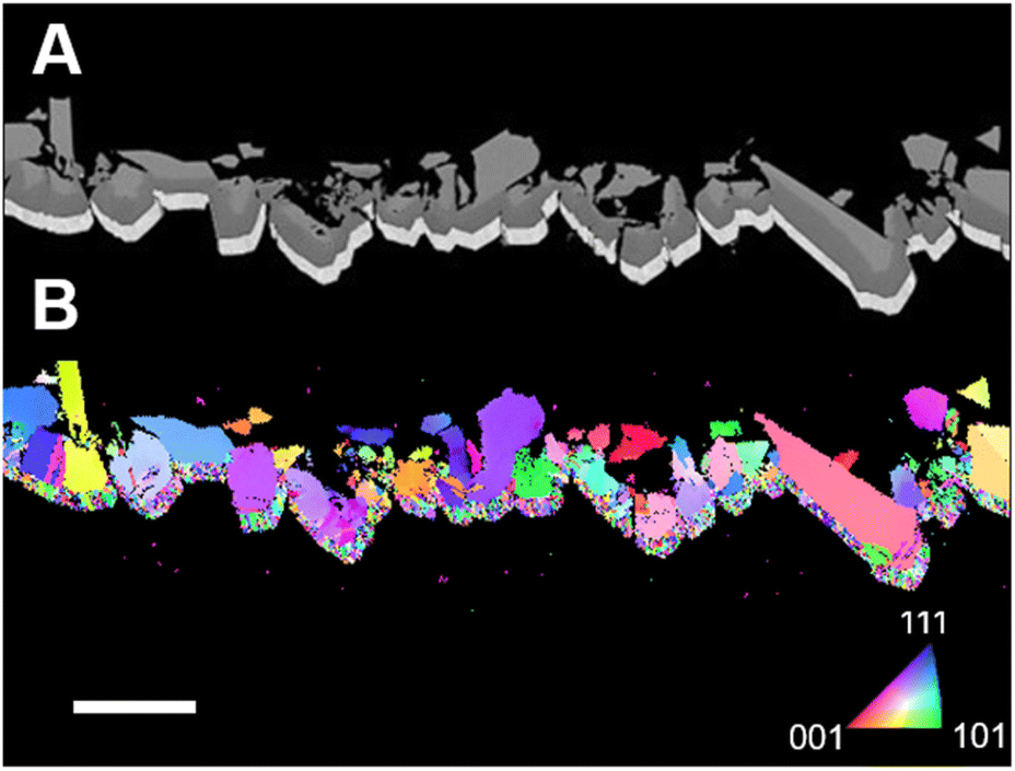 | ||
| Fig. 3 (A) Cross-sectional SEM image and (B) SEM-EBSD map of Au/ZnTe/CdTe. The EBSD maps are normal-direction inverse pole figures. Scale bar: 10 μm. | ||
XRD patterns for the Au/CdTe, Au/ZnTe/CdTe, and Au/Cu/ZnTe/CdTe (RTA) are presented in Fig. 4. The XRD pattern of Au/CdTe corresponds to the characteristic CdTe and Au diffraction peaks. Peaks observed at 23.8°, 39.4°, and 46.5° are assigned to diffraction from the (111), (220), and (311) planes of CdTe, respectively.26 Those observed at 38.3°, 44.5°, and 62.5° are assigned to diffraction from the (111), (200), and (220) planes of Au, respectively. The XRD patterns for Au/ZnTe/CdTe and Au/Cu/ZnTe/CdTe (RTA) are similar, showing diffraction peaks originating from ZnTe and alloys in addition to those from CdTe and Au. The diffraction peaks at 25.4°, 41.8°, and 49.7° are assigned to diffraction from the (111), (220), and (331) planes of ZnTe, respectively. Notably, the diffraction peaks for CdTe and ZnTe appear connected, suggesting substantial formation of a variable-composition solid solution, ZnxCd1−xTe (0 ≤ x ≤ 1), at the interfaces between ZnTe and CdTe.23
 | ||
| Fig. 4 XRD patterns for Au/CdTe, Au/ZnTe/CdTe, and Au/Cu/ZnTe/CdTe (RTA) at the (A) frontside and (B) backside before Au deposition. | ||
Current–potential (I–E) curves for the photocathodes composed of a Au/CdTe surface modified with CdS and Pt (Au/CdTe/CdS/Pt), a Au/ZnTe/CdTe surface modified with CdS and Pt (Au/ZnTe/CdTe/CdS/Pt), and a Au/Cu/ZnTe/CdTe (RTA) surface modified with CdS and Pt (Au/Cu/ZnTe/CdTe/CdS/Pt (RTA)) under intermittent simulated AM 1.5G sunlight are shown in Fig. 5A. The Au/CdTe/CdS/Pt photocathode showed a limited photocurrent and OP of −0.7 mA cm−2 at 0 VRHE and 0.45 VRHE, respectively. Yokoyama et al. reported that the introduction of CdS and Pt is essential for enhancing the performance of a CIGS photocathode.27 CdS, an n-type semiconductor, forms a p–n junction with CdTe, which increases the depletion-layer thickness at the solid–liquid interface. This junction facilitates charge separation and suppresses surface recombination by enabling the selective diffusion of electrons to the surface. Meanwhile, Pt acts as a cocatalyst, providing active surface sites and accelerating the hydrogen evolution reaction. As shown in Fig. S5 in the ESI,† Au/CdTe alone exhibited a low photocurrent of −0.05 mA cm−2 at 0 VRHE. Pt modification of the Au/CdTe photocathode (Au/CdTe/Pt) resulted in an approximately twofold increase in the photocurrent to −0.09 mA cm−2 at 0 VRHE as Pt catalyzed the water reduction. However, the observed photocurrent was still limited. The CdS-modified Au/CdTe photocathode (Au/CdTe/CdS) showed a limited photocurrent of −0.07 mA cm−2 at 0 VRHE. However, Au/CdTe/CdS/Pt showed a greater than seven-fold increase in photocurrent compared with the Au/CdTe photocathode, confirming that these surface modifications synergistically enhance the charge separation and catalytic activity of the photocathode.
 | ||
| Fig. 5 (A) Current–potential curves for photocathodes prepared from Au/CdTe/CdS/Pt, Au/ZnTe/CdTe/CdS/Pt, and Au/Cu/ZnTe/CdTe/CdS/Pt (RTA). (B) HC–STH curves calculated from the current–potential curves for Au/CdTe/CdS/Pt, Au/ZnTe/CdTe/CdS/Pt, and Au/Cu/ZnTe/CdTe/CdS/Pt (RTA). Measurements were conducted under chopped simulated sunlight in a 1 M aqueous KPi solution whose pH was adjusted to 6.5. The applied potential was swept at +10 mV s−1. | ||
As observed for the Au/ZnTe/CdTe/CdS/Pt photocathode, introducing a ZnTe layer resulted in sixfold and 0.2 V increases in the photocurrent and OP to −4.1 mA cm−2 at 0 VRHE and 0.7 VRHE, respectively. The effect of introducing ZnTe is evident in the substantial change in Rs. The Rs values were calculated from the gradient of the I–E curves at 0.3 VRHE for Au/CdTe/CdS/Pt and at 0.45 VRHE for Au/ZnTe/CdTe/CdS/Pt to be 6.1 kΩ and 0.53 kΩ, respectively. This difference in Rs is attributed to the different interfacial structure between Au/CdTe and Au/ZnTe/CdTe. The Au/CdTe interface is random because the CdTe particles are unarranged, resulting in the formation of a defective Au/CdTe interface containing voids (Fig. 2A). However, the Au/ZnTe interface is composed of straight lines (Fig. 2B) because the surface of the CSS-deposited ZnTe is composed of crystal facets (Fig. S6†) in addition to the dense interface between ZnTe and CdTe in Au/ZnTe/CdTe/CdS/Pt. As a result, the introduction of a ZnTe layer substantially reduces the Rs value. Cross-sectional SEM-EDS analysis reveals that the Zn/(Zn + Cd) ratio of the composition gradient structure increases as the structure approaches the Au back contact (Fig. 2G). According to the PESA results shown in Fig. S26 in the ESI,† the VBM potentials of Au/CdTe and Au/ZnTe/CdTe samples do not show a significant difference, indicating that the VBM potential at the surface for both Au/CdTe and Au/ZnTe/CdTe is not changed by introducing the ZnTe layer. On the other hand, ZnTe shows a comparable VBM potential of 5.3 eV to CdTe, 5.2 eV.13,23 However, the bandgap of ZnTe, 2.2 eV, is significantly larger than that of CdTe, 1.5 eV. Consequently, the composition gradient leads to the formation of a downward CBM gradient toward the photocathode surface, in addition to the band bending at the solid–liquid interface as summarized in Fig. S7 in the ESI.† This favorable band alignment is expected to contribute to the increase of the cathodic photocurrent through elongation of the lifetime of photoexcited carriers through enhanced charge separation as observed in the photocurrent decay measurement results shown in Fig. S32 in the ESI.† The effects of the band alignment on the PEC performance will be discussed later in detail.
To lower the Rs value, we examined the effect of Cu addition. The Au/Cu/ZnTe/CdTe/CdS/Pt (RTA) photocathode showed a substantially greater photocurrent of −7.0 mA cm−2 at 0 VRHE compared with that of Au/ZnTe/CdTe/CdS/Pt. The photocurrent of this photocathode surpassed that of Au/ZnTe/CdTe/CdS/Pt at 0–0.5 VRHE, whereas the OP and Rs values of the Au/Cu/ZnTe/CdTe/CdS/Pt (RTA) photocathode, 0.7 VRHE and 0.49 kΩ, respectively, were comparable to those of the Au/ZnTe/CdTe/CdS/Pt photocathode, 0.7 VRHE and 0.53 kΩ, respectively. For enhancing the cathodic photocurrent, the post RTA treatment under appropriate conditions is indispensable; the photocathode with a Cu layer introduced and prepared without an RTA treatment (Au/Cu/ZnTe/CdTe/CdS/Pt) showed a photocurrent similar to that of the photocathode without a Cu layer introduced, Au/ZnTe/CdTe/CdS/Pt (Fig. S8 and S9 in the ESI†). An increase in the hole concentration in both ZnTe and CdTe by Cu addition has been reported, and the enhanced photocurrent resulting from the post RTA treatment is due to the increase in the hole concentration, especially around the Au/ZnTe interface, as evidenced by the decrease of Rs.13,19 Post-deposition RTA treatment has also been shown to improve CdTe-based photovoltaic devices by passivating defects and activating Cu diffusion into the ZnTe and CdTe layers. SEM-EDS analysis did not detect the presence of Cu at the Au/ZnTe interface in the Au/Cu/ZnTe/CdTe/CdS/Pt (RTA) photocathode as shown in Fig. 2F, suggesting that Cu diffused into the adjacent semiconductor layers. It is reported that Cu exists in oxidation states between +1 and +2 after diffusion and behaves as an acceptor.34 Hall measurement confirmed that Cu addition improved conductivity of ZnTe and CdTe as summarized in Fig. S33 in the ESI.† The increase in the hole concentration induced by the Cu doping leads to a reduction of series resistance through increased conductivity of ZnTe and CdTe layers and thinning of the barrier can be formed at the Au/ZnTe interface.21 Notably, the XRD pattern did not substantially change at the optimal RTA temperature of 300 °C, whereas the RTA treatments at 400 and 500 °C led to a clear change in the XRD pattern compared with that for the material before RTA (Fig. S10 in the ESI†).35 XRD peaks assignable to the ZnxCd1−xTe solid solution were observed at angles intermediate between the angles of peaks for CdTe and ZnTe; for example, the ZnTe and CdTe (220) diffraction peaks observed at 41.8° and 44.5° and the ZnTe and CdTe (311) diffraction peaks observed at 46.5° and 49.7° became more intense when the RTA temperature was greater than 400 °C, indicating that interdiffusion between ZnTe and CdTe was substantially enhanced at temperatures greater than 400 °C. The HC–STH curves obtained from I–E curves are shown in Fig. 5B. The maximum HC–STH values for Au/CdTe/CdS/Pt, Au/ZnTe/CdTe/CdS/Pt, and Au/Cu/ZnTe/CdTe/CdS/Pt (RTA) were 0.06% at 0.16 VRHE, 0.64% at 0.28 VRHE, and 1.1% at 0.28 VRHE, respectively. The maximum HC–STH value of Au/Cu/ZnTe/CdTe/CdS/Pt (RTA) was more than 18 times greater than that of Au/CdTe/CdS/Pt. Notably, among the particulate photocathodes, Au/Cu/ZnTe/CdTe/CdS/Pt (RTA) exhibits a HC–STH efficiency similar to that for the (ZnSe)0.85(CuIn0.7Ga0.3Se2)0.15 particulate photocathode, whose HC–STH efficiency is the highest reported to date as summarized in Table S4 in the ESI.†![[thin space (1/6-em)]](https://www.rsc.org/images/entities/char_2009.gif) 28 Moreover, it is worth noting that the particulate photocathode exhibits a comparable photocurrent and a higher onset potential compared to most of the thin film CdTe-based photocathodes (please see Table S5 in the ESI†). The IPCE spectra of these photocathodes (i.e., Au/CdTe/CdS/Pt, Au/ZnTe/CdTe/CdS/Pt, and Au/Cu/ZnTe/CdTe/CdS/Pt (RTA)) at 0 VRHE are plotted in Fig. 6. The spectrum of Au/CdTe/CdS/Pt shows a relatively low maximum IPCE value of 5.3% at 520 nm. Notably, all of the photocathodes show a decrease in IPCE with increasing wavelength in the region below 520–540 nm, and the decrease is attributed to light absorption by the CdS layer. Interestingly, a small peak of IPCE is observed at ∼800 nm. This IPCE peak might be caused by enhanced charge collection as a result of the greater penetration depth at longer wavelengths. Because the photocathode is composed of large particles, short-wavelength light will be absorbed near the surface, whereas longer-wavelength light will be absorbed in deeper parts. As a result, the photoexcited carriers generated by longer-wavelength light increase Rs (Table S2 in the ESI†); thus, the IPCE value increases when the wavelength of incident light is ∼800 nm. However, because the optical absorption coefficient decreases with increasing wavelength, the IPCE value begins to decrease with increasing wavelength after the value reaches a local maximum. In the case of Au/ZnTe/CdTe/CdS/Pt, IPCE values were substantially increased compared with those of Au/CdTe/CdS/Pt and the maximum IPCE value was increased to 18.5% at 540 nm from only 5.4% at 540 nm by the introduction of the ZnTe layer. The IPCE spectrum of Au/ZnTe/CdTe/CdS/Pt shows similar features (i.e., a decrease at wavelengths shorter than 540 nm and a local maximum at ∼800 nm) to the spectrum of Au/CdTe/CdS/Pt because of light absorption by the CdS layer and a decrease of Rs by the photoexcited carrier. The monotonic decrease in the IPCE at 540–760 nm can be caused by the composition gradient structure, and a similar trend has been reported in the case of a thin-film photocathode.23 However, the trend is more significant in the case of this Au/ZnTe/CdTe/CdS/Pt. This sharp decrease in IPCE is attributable to the non-negligible presence of ZnTe and ZnxCd1−xTe on the photocathode surface. The UV–vis DRS spectra (Fig. S11 and S27 in the ESI†) show that Au/ZnTe/CdTe exhibits a slight decrease in light absorption from 700 to 800 nm, suggesting that ZnxCd1−xTe contributes to light absorption. Consequently, Au/ZnTe/CdTe/CdS/Pt shows a monotonic decrease in the IPCE with increasing wavelength.
28 Moreover, it is worth noting that the particulate photocathode exhibits a comparable photocurrent and a higher onset potential compared to most of the thin film CdTe-based photocathodes (please see Table S5 in the ESI†). The IPCE spectra of these photocathodes (i.e., Au/CdTe/CdS/Pt, Au/ZnTe/CdTe/CdS/Pt, and Au/Cu/ZnTe/CdTe/CdS/Pt (RTA)) at 0 VRHE are plotted in Fig. 6. The spectrum of Au/CdTe/CdS/Pt shows a relatively low maximum IPCE value of 5.3% at 520 nm. Notably, all of the photocathodes show a decrease in IPCE with increasing wavelength in the region below 520–540 nm, and the decrease is attributed to light absorption by the CdS layer. Interestingly, a small peak of IPCE is observed at ∼800 nm. This IPCE peak might be caused by enhanced charge collection as a result of the greater penetration depth at longer wavelengths. Because the photocathode is composed of large particles, short-wavelength light will be absorbed near the surface, whereas longer-wavelength light will be absorbed in deeper parts. As a result, the photoexcited carriers generated by longer-wavelength light increase Rs (Table S2 in the ESI†); thus, the IPCE value increases when the wavelength of incident light is ∼800 nm. However, because the optical absorption coefficient decreases with increasing wavelength, the IPCE value begins to decrease with increasing wavelength after the value reaches a local maximum. In the case of Au/ZnTe/CdTe/CdS/Pt, IPCE values were substantially increased compared with those of Au/CdTe/CdS/Pt and the maximum IPCE value was increased to 18.5% at 540 nm from only 5.4% at 540 nm by the introduction of the ZnTe layer. The IPCE spectrum of Au/ZnTe/CdTe/CdS/Pt shows similar features (i.e., a decrease at wavelengths shorter than 540 nm and a local maximum at ∼800 nm) to the spectrum of Au/CdTe/CdS/Pt because of light absorption by the CdS layer and a decrease of Rs by the photoexcited carrier. The monotonic decrease in the IPCE at 540–760 nm can be caused by the composition gradient structure, and a similar trend has been reported in the case of a thin-film photocathode.23 However, the trend is more significant in the case of this Au/ZnTe/CdTe/CdS/Pt. This sharp decrease in IPCE is attributable to the non-negligible presence of ZnTe and ZnxCd1−xTe on the photocathode surface. The UV–vis DRS spectra (Fig. S11 and S27 in the ESI†) show that Au/ZnTe/CdTe exhibits a slight decrease in light absorption from 700 to 800 nm, suggesting that ZnxCd1−xTe contributes to light absorption. Consequently, Au/ZnTe/CdTe/CdS/Pt shows a monotonic decrease in the IPCE with increasing wavelength.
 | ||
| Fig. 6 IPCE spectra obtained for Au/CdTe/CdS/Pt, Au/ZnTe/CdTe/CdS/Pt, and Au/Cu/ZnTe/CdTe/CdS/Pt (RTA) photocathodes at 0 VRHE under monochromatic light. | ||
The enhanced IPCE values observed for photocathodes incorporating the ZnTe layer are attributable to the charge separation mechanism being dependent on the light absorption region, as summarized in Fig. S12 in the ESI.† As confirmed in Fig. S13 in the ESI,† the interdiffusion between ZnTe and CdTe particles forms a ∼1 μm-thick ZnxCd1−xTe layer with a composition gradient from the interface into the CdTe particle. Notably, the underlayer, nominally the ZnTe layer, is largely occupied by the ZnxCd1−xTe layer with a composition gradient, which forms by interdiffusion between CdTe and ZnTe. As shown in Fig. S13 in the ESI,† the effective thickness of the CdTe layer is sensitive to the particle size. The particle size is less than 5 μm, resulting in photocathodes in which the effective thickness of pure CdTe (L) ranges from 0 to 4 μm. According to the simulation results in Fig. S14 in the ESI,† the charge separation mechanism can be categorized into three different cases: (1) large particles with L > 3 μm, (2) intermediate-sized particles with 0 < L < μm, and (3) small particles occupied by ZnxCd1−xTe with a composition gradient (L = 0). To better understand how these structural modifications influence charge collection, we conducted simulations to obtain the band diagram and evaluate the relationship between total recombination (rtotal) and L at wavelengths of 400, 600, and 800 nm (Fig. S13 in the ESI†). Notably, as a consequence of the absorption coefficient of CdTe, the photoexcited carriers are generated within 3 μm of the surface (Fig. S15 in the ESI†).
For large particles (L > 3 μm), the generation of photoexcited carriers occurs in the pure CdTe layer and the change in rtotal is limited against L. In this case, the ZnxCd1−xTe underlayer primarily functions as a hole-selective back contact because the CBM of ZnxCd1−xTe is shallower than that of CdTe. However, a limited number of photoexcited carriers can reach the back contact; the enhancement of the hydrogen evolution is limited as a consequence. Notably, even though charge generation mainly occurs in the CdTe layer, the recombination rate was suppressed in ZnxCd1−xTe because of the existence of the composition gradient (Fig. S16 in the ESI†).
As the CdTe layer becomes thinner (0 < L < 3 μm), the photoexcited carriers are generated in the pure CdTe layer and partially in the ZnxCd1−xTe layer. According to the simulation results in Fig. S13 and S14 in the ESI,†rtotal decreases with decreasing L in the case of 800 nm light because long-wavelength light can reach the ZnxCd1−xTe layer. By contrast, in the cases of 400 and 600 nm light, the light is absorbed within 1 μm and the ZnxCd1−xTe layer only acts as a hole-selective back contact, leading to minimal changes in the rtotal values. With a further decrease in the CdTe layer thickness (L < 0.5 μm), photoexcited carriers are generated in both the pure CdTe and ZnxCd1−xTe layers at all wavelengths, resulting in a noticeable reduction in rtotal. Interestingly, a substantial decrease occurs when the particles are smaller than 1 μm (L = 0), where all of the CdTe particles become ZnxCd1−xTe with a composition-gradient structure, resulting in a one-order-of-magnitude reduction in rtotal, effectively suppressing charge recombination.
In comparison with the Au/CdTe/CdS/Pt and Au/ZnTe/CdTe/CdS/Pt photocathodes, the Au/Cu/ZnTe/CdTe/CdS/Pt (RTA) photocathodes exhibited clearly higher IPCEs across the whole spectrum. The Au/Cu/ZnTe/CdTe/CdS/Pt (RTA) photocathodes exhibit a maximum IPCE value of 36% at 520 nm, which is the highest IPCE value reported thus far for a particulate photocathode, with >10% IPCE in a wide wavelength range of 440–840 nm. On the basis of these IPCE values, the expected photocurrent under AM 1.5G light is 6.8 mA cm−2 for Au/Cu/ZnTe/CdTe/CdS/Pt (RTA), consistent with the current–potential curve shown in Fig. 4. We concluded that the composition gradient structure is clearly advantageous for photoelectrochemical and photocatalytic water-splitting reactions.
To confirm the faradaic efficiency of the Au/Cu/ZnTe/CdTe/CdS/Pt (RTA) photocathode, we used a microGC to measure the amounts of H2 and O2 evolved under irradiation with an applied potential of 0 VRHE. As shown in Fig. 7, we confirmed stoichiometric water splitting with faradaic efficiencies for H2 and O2 evolution of almost 100%, whereas the time course of photocurrent indicates durable H2 evolution for 1 h. To assess the durability for a relatively long period, the time course of the photocurrent for 21 h was measured, and the result shown in Fig. S28 in the ESI† indicates that the photocathode works longer than the period. However, the cathodic photocurrent consequently decreased to be −1.7 mA cm−2 after the reaction for 21 h. The XPS analysis results shown in Fig. S29 and S30 in the ESI† revealed that the degradation is mainly because of detachment of Pt.
 | ||
| Fig. 7 (A) Hydrogen and oxygen evolution and (B) time course of the photocurrent for the Au/Cu/ZnTe/CdTe/CdS/Pt (RTA) photocathode under simulated sunlight in a three-electrode configuration with an applied potential of 0 VRHE. The expected amounts of hydrogen and oxygen (denoted as e−/2 and e−/4, respectively), as calculated from the observed photocurrent, are shown as dashed lines. A 1 M aqueous KPi solution whose pH was adjusted to 6.5 by addition of KOH was used as the electrolyte. The photoelectrode area was 0.488 cm−2. | ||
Finally, we demonstrated overall PEC water splitting using a Au/Cu/ZnTe/CdTe/CdS/Pt photocathode coupled with a Nb:STO based photoanode. The photoanode was positioned in front of the photocathode and the device was illuminated with AM 1.5G simulated sunlight without applying external bias voltage. As shown in Fig. S31A in the ESI,† current–potential curves of the photocathode and photoanode are overlapped, and current matching is satisfied at 0.4 VRHE, indicating the capability of unbiased PEC water splitting. Fig. S31B in the ESI† confirms stoichiometric evolution of H2 and O2, with a 2:1 molar ratio, validating overall water splitting using the constructed PEC cell. Based on these results, the solar-to-hydrogen conversion efficiency of the tandem PEC device was estimated to be 0.2%, which aligns with the photocurrent limitations imposed by the Nb:STO photoanode. Future work should focus on optimizing the deposition parameters to improve the CdTe surface coverage and on integration with an O2 evolution reaction system which has an absorption edge in the visible light region to construct an efficient unbiased water splitting device.
Conclusion
In this study, we constructed a novel photocathode composed of photocatalytic particles with an induced composition gradient. The effects of the composition gradient were assessed on the basis of the experimental and simulation results, and the IPCE and HC–STH were the highest reported thus far: 36% at 520 nm and 1.1% at 0.28 VRHE, respectively. The novel structured photocathode was prepared using a modified particle transfer method. In this method, a 3 μm-thick ZnTe layer deposited via the CSS method was used as a contact layer to form a contact method preferable to particulate CdTe for selective extraction of holes to the Au back contact. Interestingly, the ZnTe contact layer formation process resulted in the growth of ZnTe on CdTe particles. Moreover, ZnxCd1−xTe was also formed through the interdiffusion between CdTe particles and the ZnTe layer. With optimization of the substrate temperature, the ZnxCd1−xTe formed between the particulate CdTe and the ZnTe layer resulted in an appropriate composition gradient that enhanced charge separation. The photocathode prepared under optimized conditions with the composition gradient showed an approximately six-fold enhanced photocurrent of −4.1 mA cm−2 at 0 VRHE and positively shifted the onset potential of the cathodic photocurrent by +0.2 VRHE to 0.7 VRHE compared with the cathodic photocurrent of the Au/CdTe/CdS/Pt photocathode (see Fig. S5 in the ESI†). According to the simulation, the formation of ZnxCd1−xTe with a composition gradient produces a CBM gradient that enhances the charge separation, indicating suppression of charge recombination. Further incorporation of a Cu layer and application of a post RTA treatment substantially improved PEC hydrogen evolution, increasing the photocurrent to −7 mA cm−2 at 0 VRHE. This improvement was attributed to enhanced electrical properties, such as a decreased Rs and an associated reduction of the height of the Schottky barrier formed at the Au–ZnTe interface. Consequently, among the investigated particulate photocathodes, the Au/Cu/ZnTe/CdTe/CdS/Pt (RTA) photocathode prepared under optimized conditions demonstrated the highest HC-STH value of 1.1% at 0.28 VRHE and a high level of IPCE value of 36% at 520 nm, with >10% IPCE over the 440–800 nm range. We expect the results of this study to provide guidance in the development of efficient particulate photoelectrodes and photocatalysts by introduction of composition gradients.Data availability
The data supporting this article have been included as part of the ESI.†Author contributions
T. Minegishi led the research project. M. Sugiyama and T. Minegishi supervised the experimental work. L. S. Veiga prepared, characterized and analysed the photoelectrodes. M. Nakabayashi prepared the cross-section samples and the EBSD measurements. T. Fujii conducted the Hall effect measurements. T. Minegishi and L. S. Veiga discussed the results and wrote the manuscript with contributions from the other authors. All authors reviewed the manuscript.Conflicts of interest
The authors declare no competing financial interest.Acknowledgements
This work was supported by Grants-in-Aid for Scientific Research (A) (No. JP21H04551) from the Japan Society for the Promotion of Science (JSPS). A part of this work was supported by the “Advanced Research Infrastructure for Materials and Nanotechnology in Japan (ARIM)” of the Ministry of Education, Culture, Sports, Science and Technology (MEXT) (grant no. JPMXP1222UT0248, JPMXP1223UT0039 and JPMXP1225UT0149). Hall effect measurements were performed using the Physical Property Measurement System (PPMS Quantum Design) of the Cryogenic Research Center, the University of Tokyo.References
- Z. J. Baum, L. L. Diaz, T. Konovalova and Q. A. Zhou, Materials Research Directions Toward a Green Hydrogen Economy, ACS Omega, 2022, 7, 32908–32935 CrossRef CAS PubMed.
- J. H. Kim, D. Hansora, P. Sharma, J. W. Jang and J. S. Lee, Toward practical solar hydrogen production-an artificial photo-synthetic leaf-to-farm challenge, Chem. Soc. Rev., 2019, 48, 1908–1971 RSC.
- Q. Wang, T. Hisatomi, Q. Jia, H. Tokudome, M. Zhong, C. Wang, Z. Pan, T. Takata, M. Nakabayashi, N. Shibata, Y. Li, I. D. Sharp, A. Kudo, T. Yamada and K. Domen, Scalable water splitting on particulate photocatalyst sheets with a solar-to-hydrogen energy conversion efficiency exceeding 1%, Nat. Mater., 2016, 15, 611–615 CrossRef CAS PubMed.
- Y. Kageshima, Y. Goto, H. Kaneko, M. Nakabayashi, N. Shibata, K. Domen and T. Minegishi, Sunlight-Driven Production of Methylcyclohexane from Water and Toluene Using ZnSe:Cu(In,Ga)Se2-Based Photocathode, ChemCatChem, 2019, 11, 4266–4271 CrossRef CAS.
- B. Zhang, K. Liu, Y. Xiang, J. Wang, W. Lin, M. Guo and G. Ma, Facet-Oriented Assembly of Mo:BiVO4 and Rh:SrTiO3 Particles: Integration of p–n Conjugated Photoelectrochemical System in a Particle Applied to Photocatalytic Overall Water Splitting, ACS Catal., 2022, 12, 2415–2425 CrossRef CAS.
- Q. Wang, T. Hisatomi, Y. Suzuki, Z. Pan, J. Seo, M. Katayama, T. Minegishi, H. Nishiyama, T. Takata, K. Seki, A. Kudo, T. Yamada and K. Domen, Particulate photocatalyst sheets based on carbon conductor layer for efficient Z-scheme pure-water splitting at ambient pressure, J. Am. Chem. Soc., 2017, 139, 1675–1683 CrossRef CAS PubMed.
- H. Kaneko, T. Minegishi and K. Domen, Recent Progress in the Surface Modification of Photoelectrodes toward Efficient and Stable Overall Water Splitting, Chem.–Eur. J, 2018, 24, 5697–5706 CrossRef CAS.
- J. Yang, D. Wang, H. Han and C. Li, Roles of cocatalysts in photocatalysis and photoelectrocatalysis, Acc. Chem. Res., 2013, 46, 1900–1909 CrossRef CAS.
- J. X. Jian, L. H. Xie, A. Mumtaz, T. Baines, J. D. Major, Q. X. Tong and J. Sun, Interface-Engineered Ni-Coated CdTe Heterojunction Photocathode for Enhanced Photoelectrochemical Hydrogen Evolution, ACS Appl. Mater. Interfaces, 2023, 15, 21057–21065 CrossRef CAS PubMed.
- J. Su, T. Minegishi, M. Katayama and K. Domen, Photoelectrochemical hydrogen evolution from water on a surface modified CdTe thin film electrode under simulated sunlight, J. Mater. Chem. A, 2017, 5, 4486–4492 RSC.
- H. Kumagai, T. Minegishi, N. Sato, T. Yamada, J. Kubota and K. Domen, Efficient solar hydrogen production from neutral electrolytes using surface-modified Cu(In,Ga)Se2 photocathodes, J. Mater. Chem. A, 2015, 3, 8300–8307 RSC.
- M. Moriya, T. Minegishi, H. Kumagai, M. Katayama, J. Kubota and K. Domen, Stable Hydrogen Evolution from CdS-Modified CuGaSe2 Photoelectrode under Visible-Light Irradiation, JACS, 2013, 3733–3735 CrossRef CAS.
- T. Minegishi, A. Ohnishi, Y. Pihosh, K. Hatagami, T. Higashi, M. Katayama, K. Domen and M. Sugiyama, ZnTe-based photocathode for hydrogen evolution from water under sunlight, APL Mater., 2020, 9, 041101 CrossRef.
- H. Kobayashi, N. Sato, M. Orita, Y. Kuang, H. Kaneko, T. Minegishi, T. Yamada and K. Domen, Development of highly efficient CuIn0.5Ga0.5Se2-based photocathode and application to overall solar driven water splitting, Energy Environ. Sci., 2018, 11, 3003–3009 RSC.
- J. Zhao, T. Minegishi, L. Zhang, M. Zhong, Gunawan, M. Nakabayashi, G. Ma, T. Hisatomi, M. Katayama, S. Ikeda, N. Shibata, T. Yamada and K. Domen, Enhancement of solar hydrogen evolution from water by surface modification with CdS and TiO2 on porous CuInS2 photocathodes prepared by an electrodeposition-sulfurization method, Angew. Chem., Int. Ed., 2014, 53, 11808–11812 CrossRef CAS PubMed.
- Y. Goto, T. Minegishi, Y. Kageshima, T. Higashi, H. Kaneko, Y. Kuang, M. Nakabayashi, N. Shibata, H. Ishihara, T. Hayashi, A. Kudo, T. Yamada and K. Domen, A particulate (ZnSe)0.85(CuIn0.7Ga0.3Se2)0.15 photocathode modified with CdS and ZnS for sunlight-driven overall water splitting, J. Mater. Chem. A, 2017, 5, 21242–21248 RSC.
- T. Minegishi, S. Yamaguchi and M. Sugiyama, Efficient hydrogen evolution from water over thin film photocathode com-posed of solid solutions between ZnSe and Cu(In, Ga)Se2 with composition gradient, Appl. Phys. Lett., 2021, 119, 123905 CrossRef CAS.
- C. Britt and J. Ferekides, Thin-film CdS/CdTe solar cell with 15.8% efficiency, Appl. Phys. Lett., 1993, 62, 2851 CrossRef.
- J. Su, T. Minegishi and K. Domen, Efficient hydrogen evolution from water using CdTe photocathodes under simulated sunlight, J. Mater. Chem. A, 2017, 5, 13154–13160 RSC.
- J. Li, D. R. Diercks, T. R. Ohno, C. W. Warren, M. C. Lonergan, J. D. Beach and C. A. Wolden, Controlled activation of ZnTe:Cu contacted CdTe solar cells using rapid thermal processing, Sol. Energy Mater. Sol. Cells, 2015, 133, 208–215 CrossRef CAS.
- K. Shen, X. Wang, Y. Zhang, H. Zhu, Z. Chen, C. Huang and Y. Mai, Insights into the role of interface modification in performance enhancement of ZnTe:Cu contacted CdTe thin film solar cells, Sol. Energy, 2020, 201, 55–62 CrossRef CAS.
- K. Bashir, N. Mehboob, A. Ali, A. Zaman, M. Ashraf, M. Lal, K. Althubeiti and M. Mushtaq, Fabrication and characterization of Cd1-xZnxTe thin films for photovoltaic applications, Mater. Lett., 2021, 304, 130737 CrossRef CAS.
- L. S. Veiga, H. Kumagai, M. Sugiyama and T. Minegishi, Efficient hydrogen evolution from water over a thin film photocathode composed of solid solutions with a composition gradient of ZnTe and CdTe, Sustainable Energy Fuels, 2024, 8, 2210–2218 RSC.
- Y. Asakura, T. Higashi, H. Nishiyama, H. Kobayashi, M. Nakabayashi, N. Shibata, T. Minegishi, T. Hisatomi, M. Katayama, T. Yamada and K. Domen, Activation of a particulate Ta3N5 water-oxidation photoanode with a GaN hole-blocking layer, Sustainable Energy Fuels, 2018, 2, 73–78 RSC.
- T. Minegishi, N. Nishimura, J. Kubota and K. Domen, Photoelectrochemical properties of LaTiO2N electrodes prepared by particle transfer for sunlight-driven water splitting, Chem. Sci., 2013, 4, 1120–1124 RSC.
- J. Moseley, W. K. Metzger, H. R. Moutinho, N. Paudel, H. L. Guthrey, Y. Yan, R. K. Ahrenkiel and M. M. Al-Jassim, Recombination by grain-boundary type in CdTe, J. Appl. Phys., 2015, 118, 025702 CrossRef.
- D. Yokoyama, T. Minegishi, K. Maeda, M. Katayama, J. Kubota, A. Yamada, M. Konagai and K. Domen, Photoelectrochemical water splitting using a Cu(In,Ga)Se2 thin film, Electrochem. Commun., 2010, 12, 851–853 CrossRef CAS.
- Y. Kageshima, T. Minegishi, Y. Goto, H. Kaneko and K. Domen, Particulate photocathode composed of (ZnSe)0.85(CuIn0.7Ga0.3Se2)0.15 synthesized with Na2S for enhanced sunlight-driven hydrogen evolution, Sustainable Energy Fuels, 2018, 2, 1957–1965 RSC.
- G. Liang, Z. Li, M. Ishaq, Z. Zheng, Z. Su, H. Ma, X. Zhang, P. Fan and S. Chen, Charge Separation Enhancement Enables Record Photocurrent Density in Cu2ZnSn(S,Se)4 Photocathodes for Efficient Solar Hydrogen Production, Adv. Energy Mater., 2023, 13, 2300215 CrossRef CAS.
- W. Chen, D. Wang, W. Wang, X. Liu, Y. Liu, C. Wang, Y. Kang, S. Fang, X. Yang, W. Gu, D. Luo, Y. Luo, Z. Qu, C. Zuo, Y. Kang, L. Cheng, W. Yan, W. Hu, R. Long, J.-H. He, K. Liang, S. Liu, Y. Xiong and H. Sun, Enhanced solar hydrogen production via reconfigured semi-polar facet/cocatalyst heterointerfaces in GaN/Si photocathodes, Nat. Commun., 2025, 16, 879 CrossRef CAS.
- Y. Xiao, X. Kong, S. Vanka, W. J. Dong, G. Zeng, Z. Ye, K. Sun, I. A. Navid, B. Zhou, F. M. Toma, H. Guo and Z. Mi, Oxynitrides enabled photoelectrochemical water splitting with over 3,000 hrs stable operation in practical two-electrode configuration, Nat. Commun., 2023, 14, 2047 CrossRef CAS.
- H. Fu, Y. Wu, Y. Guo, T. Sakurai, Q. Zhang, Y. Liu, Z. Zheng, H. Cheng, Z. Wang, B. Huang, Q. Wang, K. Domen and P. Wang, A scalable solar-driven photocatalytic system for separated H2 and O2 production from water, Nat. Commun., 2025, 16, 990 CrossRef CAS PubMed.
- Y. Kageshima, Y. Goto, H. Kaneko, M. Nakabayashi, N. Shibata, K. Domen and T. Minegishi, Sunlight-Driven Production of Methylcyclohexane from Water and Toluene Using ZnSe : Cu(In,Ga)Se2-Based Photocathode, ChemCatChem, 2019, 11, 4266–4271 ( Chem. Commun. , 2017 , 53 , 11674–11677 ) CrossRef CAS.
- S. Rojsatien, A. Mannodi-Kanakkithodi, T. Walker, N. Mohan Kumar, T. Nietzold, E. Colegrove, D. Mao, M. E. Stuckelberger, B. LaI, Z. Cai, M. K. Y. Chan and M. I. Bertoni, Distribution of Copper States, Phases, and Defects across the Depth of a Cu-Doped CdTe Solar Cell, Chem. Mater., 2023, 35, 9935–9944 CrossRef CAS.
- T. Higashi, H. Kaneko, T. Minegishi, H. Kobayashi, M. Zhong, Y. Kuang, T. Hisatomi, M. Katayama, T. Takat, H. Nishiyama, T. Yamada and K. Domen, Overall water splitting by photoelectrochemical cells consisting of (ZnSe)0.85(CuIn0.7Ga0.3Se2)0.15 photocathodes and BiVO4 photoanodes, Chem. Commun., 2017, 53, 11674–11677 RSC.
Footnote |
| † Electronic supplementary information (ESI) available: Material characterization via SEM, SEM-EDS, XRD, and UV-vis DRS, simulation of the band diagram, charge generation and charge re-combination, and description of performance optimization by varying the ZnTe deposition time and temperature source. See DOI: https://doi.org/10.1039/d5sc02472b |
| This journal is © The Royal Society of Chemistry 2025 |