
 Open Access Article
 This Open Access Article is licensed under a Creative Commons Attribution-Non Commercial 3.0 Unported Licence
Iron-assisted growth of anisotropic ZnO nanostructures†
Zhengxi
Xuan
ab,
Avisek
Dutta
 cd,
Shuo
Liu
af,
Yueling
Qin
e,
Kaiwen
Chen
a,
Zheng
Fu
ab,
Paras N.
Prasad
cd,
Chaochao
Dun
*f and
Mark T.
Swihart
*ab
cd,
Shuo
Liu
af,
Yueling
Qin
e,
Kaiwen
Chen
a,
Zheng
Fu
ab,
Paras N.
Prasad
cd,
Chaochao
Dun
*f and
Mark T.
Swihart
*ab
aDepartment of Chemical and Biological Engineering, University at Buffalo, The State University of New York, Buffalo, 14226, NY, USA. E-mail: swihart@buffalo.edu
bRENEW Institute, University at Buffalo, The State University of New York, Buffalo, 14226, NY, USA
cDepartment of Chemistry, University at Buffalo, The State University of New York, Buffalo, 14226, NY, USA
dDepartment of Chemistry, Institute for Lasers, Photonics, and Biophotonics, The State University of New York, Buffalo, 14226, NY, USA
eDepartment of Physics, University at Buffalo, The State University of New York, Buffalo, New York, 14260, USA
fThe Molecular Foundry, Lawrence Berkeley National Lab, Berkeley, CA 94720, USA. E-mail: cdun@lbl.gov
First published on 2nd June 2025
Abstract
Anisotropic nanostructures offer a promising pathway to modulate structure–function relationships of materials. However, the correlation between growth direction of high-quality anisotropic nanostructures, the synthesis conditions and mechanisms controlling their growth, and their magnetic and optical properties remain underexplored. In this study, we developed an iron-assisted anisotropic growth method to form zinc oxide nanostructures on the O-polar (000![[1 with combining macron]](https://www.rsc.org/images/entities/char_0031_0304.gif) ) surface, resulting in two distinct ZnO-based nanostructures: hand-shaped nanostructures and truncated hexagonal nanopyramids. In contrast to most reports of anisotropic nanostructure synthesis, which primarily focus on morphology control through ligand–ligand interactions, the current study probes the effects of doping on anisotropic growth, and how doping, along with ligand–ligand interactions and facet-specific ligand binding, control nanostructure morphology. The reaction mechanisms leading to formation of these novel structures were thoroughly probed by systematically manipulating synthesis parameters. A two-step formation mechanism was identified: first, a hexagonal platform forms through an initial homogeneous nucleation process, followed by secondary heterogeneous nucleation, which results in metastable secondary nanostructures growing on the oxygen-rich template. Optical and magnetic properties of these Fe/ZnO nanostructures were characterized. Our findings provide a new strategy that uses a magnetic element as a dopant to build new nanostructures of ZnO with controllable size and shape growing on an oxygen-rich crystal plane. These materials could have applications in novel technologies where both optoelectronic and magnetic properties are of interest.
) surface, resulting in two distinct ZnO-based nanostructures: hand-shaped nanostructures and truncated hexagonal nanopyramids. In contrast to most reports of anisotropic nanostructure synthesis, which primarily focus on morphology control through ligand–ligand interactions, the current study probes the effects of doping on anisotropic growth, and how doping, along with ligand–ligand interactions and facet-specific ligand binding, control nanostructure morphology. The reaction mechanisms leading to formation of these novel structures were thoroughly probed by systematically manipulating synthesis parameters. A two-step formation mechanism was identified: first, a hexagonal platform forms through an initial homogeneous nucleation process, followed by secondary heterogeneous nucleation, which results in metastable secondary nanostructures growing on the oxygen-rich template. Optical and magnetic properties of these Fe/ZnO nanostructures were characterized. Our findings provide a new strategy that uses a magnetic element as a dopant to build new nanostructures of ZnO with controllable size and shape growing on an oxygen-rich crystal plane. These materials could have applications in novel technologies where both optoelectronic and magnetic properties are of interest.
Introduction
Colloidal nanocrystals (NCs) represent an important class of nanomaterials with structure–property relationships that are tunable through shape and composition modifications controlled by growth conditions and interactions with ligands bound to their surfaces.1–3 Achieving uniformity in the size, shape and crystalline structure of NCs is essential for a variety of applications.4,5 For example, the exposure of certain crystal facets can enhance selectivity or activity in photocatalysis,6–8 thermocatalysis,9,10 and gas sensing.11,12 Moreover, the size of these NCs plays a significant role in electronic structure modulation via quantum confinement and plasmonic effects.13–15 The phase behavior of NCs can be tuned by modifying their geometry and free energy through interaction with surface ligands, as predicted by computational simulations,16 resulting a rich diversity of particles shape with distinctive properties.Nanocrystals of wurtzite-phase materials, including ZnO, ZnS, CdSe and GaN, exhibit useful semiconducting properties originating from their wide electronic band gaps.17,18 The remarkable optical features of these materials can be shape-dependent, and they have a propensity for anisotropic growth along their crystallographically distinct c-axis. This propensity can be exploited. For instance, exposure of the (0001) and (0110) planes significantly impacts photocatalytic performance,6,7 while surfaces dominated by the (100), (0001) and (101) planes amplified surface-enhanced Raman scattering (SERS).19,20 Although most facet exposure is controlled by adjusting ligand–ligand interactions during colloidal synthesis, there is a lack of detailed synthesis routes for heterogeneous atom-doped wurtzite structures that provide specific crystal facet exposure. Incorporation of heteroatoms into wurtzite nanocrystals can also result in binary solid solutions with tunable magnetic21,22 and optical anisotropy.17 Additionally, heterogeneous atom doping can induce the formation of vacancies, enhancing paramagnetic resonance and photoluminescence.23,24
Here, we report the shape-controllable, iron-assisted growth of wurtzite ZnO in ordered nanostructures of unique morphologies. As a transition metal with unpaired 3d electrons, Fe introduces localized magnetic moments and therefore promotes sp–d exchange interactions within the ZnO lattice, making it a promising candidate for the design of magnetic semiconductors. Nucleation and growth of ZnO were favored on the low index oxygen-rich crystal plane (000) in the c-axis direction by manipulating ligand–ligand interactions and reaction temperature. Two unusual Fe-doped-ZnO nanostructures were formed: hand-shaped nanostructures consisting of hexagonal plate-like ZnO “palms” with “fingers” growing from them, and truncated hexagonal pyramid nanostructures, where an initial hexagonal prism of ZnO was surrounded by a metastable, branch-like outer shell. Both structures were grown with Fe heteroatoms doped into the ZnO crystal lattice, which induced initial lateral growth, perpendicular to the c-axis. This was followed by continued growth along the c-axis, terminated at the Zn-rich crystal plane (0001). Magnetic and optical properties were evaluated for these magnetic Fe-doped semiconducting nanostructures, revealing that anisotropic properties may arise from shape anisotropy. This study explores the complexity of the heteroatom doping and the anisotropic growth process, providing a foundation for future studies that can further explore the fundamental doping mechanism contributing to more complex processing-structure–property relationships and harness shape control for specific applications. The magnetic dopants incorporated into anisotropic ZnO nanostructures enable potential applications in areas such as optical isolators and modulators, spintronic devices, magnetic field sensors, or UV photodetectors.
Results and discussion
Growth of “hand-shaped” Fe/ZnO nanostructures
Fe/ZnO hand-shaped nanostructures were synthesized using octadecene (ODE) as solvent, with oleylamine (OAm) and myristic acid (MA) as capping ligands. These nanostructures consist of two parts; the “palm”, which forms the base, and the “fingers” that continuously grow on top of the “palm”, resulting in an overall “hand-shaped” nanostructure (Fig. 1a and b). High-angle annular darkfield scanning transmission electron microscopy (HAADF-STEM) and elemental mapping by energy-dispersive X-ray spectroscopy (STEM-EDS) confirmed a uniform distribution of Fe and Zn atoms throughout the hand-shaped system, producing a stable solid solution (Fig. 1c–f). Movie S1† presents 3D imaging and elemental mapping of the Fe/ZnO hand-shaped nanostructures, showing the “fingers” built-up upon the “palm” portion. These hand-shaped nanostructures adopt the expected ZnO hexagonal wurtzite crystal structure (P63mc, a = b = 3.2489 Å, c = 5.2049 Å) as demonstrated by powder X-ray diffraction (XRD) (Fig. S1†). Scanning electron microscopy-energy dispersive X-ray spectroscopy (SEM-EDS) analysis from two different locations gave a Fe![[thin space (1/6-em)]](https://www.rsc.org/images/entities/char_2009.gif) :Zn atomic ratio of approximately 1:16 (Fig. S2a†). However, the sum of the concentrations of Fe and Zn atoms were less than that of O atoms, suggesting the presence of a significant amount of surface adsorbed water or oxygen. X-ray photoelectron spectroscopy (XPS) (Fig. S3†) was performed to analyze the chemical state of atoms at the surface of the nanostructures. Peaks at 709.9 eV and 722.7 eV, corresponding to Fe 2p3/2 and Fe 2p1/2, respectively, are assigned to the Fe2+ oxidation state. Peaks characteristic of Fe3+ were also observed at 711.5 eV (Fe 2p3/2) and 725.6 eV (Fe 2p1/2).25,26 Additionally, in the O 1s XPS spectra, a peak at ∼531.7 eV, attributed to surface oxygen vacancies, and the lattice oxygen peak at ∼530 eV were of comparable area, suggesting approximately equal concentrations of oxygen vacancies and lattice oxygen at the surface of the Fe/ZnO hand-shaped nanostructures. The generation and control of oxygen vacancies can potentially enhance catalytic and photocatalytic activity of the nanostructures.
:Zn atomic ratio of approximately 1:16 (Fig. S2a†). However, the sum of the concentrations of Fe and Zn atoms were less than that of O atoms, suggesting the presence of a significant amount of surface adsorbed water or oxygen. X-ray photoelectron spectroscopy (XPS) (Fig. S3†) was performed to analyze the chemical state of atoms at the surface of the nanostructures. Peaks at 709.9 eV and 722.7 eV, corresponding to Fe 2p3/2 and Fe 2p1/2, respectively, are assigned to the Fe2+ oxidation state. Peaks characteristic of Fe3+ were also observed at 711.5 eV (Fe 2p3/2) and 725.6 eV (Fe 2p1/2).25,26 Additionally, in the O 1s XPS spectra, a peak at ∼531.7 eV, attributed to surface oxygen vacancies, and the lattice oxygen peak at ∼530 eV were of comparable area, suggesting approximately equal concentrations of oxygen vacancies and lattice oxygen at the surface of the Fe/ZnO hand-shaped nanostructures. The generation and control of oxygen vacancies can potentially enhance catalytic and photocatalytic activity of the nanostructures.
 | ||
| Fig. 1 Morphology characterization of two types of Fe/ZnO nanostructures. (a) TEM, (b) SEM and (c)–(f) HAADF-STEM and STEM-EDS elemental maps of hand-shaped Fe/ZnO nanostructures. (g) TEM, (h) SEM and (i)–(l) HAADF-STEM and STEM-EDS elemental maps of truncated hexagonal pyramid Fe/ZnO nanostructures. | ||
Growth of “truncated hexagonal pyramid” Fe/ZnO nanostructures
On the contrary, when using OAm as solvent, with MA as an additional ligand, truncated hexagonal pyramid Fe/ZnO nanostructures (denoted as Fe/ZnO hexagonal nanostructures) were synthesized (Fig. 1g and h). TEM images (Fig. 1g) revealed the hexagonal Fe/ZnO nanostructures consist of two parts; an inner hexagonal prism core surrounded by branch-like lateral edges of Fe-doped-zinc oxide. HAADF-STEM imaging and STEM-EDS mapping (Fig. 1i–l) confirmed a uniform distribution of Fe atoms throughout the Fe/ZnO hexagonal nanostructures. However, a lower Fe concentration was observed in the hexagonal prism core, with a higher concentration localized on the lateral sides of the prism and its extending branches. Fig. S4† provides a TEM image and corresponding SAED image showing evidence of both single crystalline and amorphous patterns, indicating two distinct regions with different formation mechanisms in the hexagonal nanostructures. SEM-EDS (Fig. S2b†) gave an atomic ratio of Fe to Zn of approximately 1:9. In contrast to the Fe/ZnO hand-shaped structures, the sum of Fe and Zn atoms in these nanostructures nearly matches the number of oxygen atoms. XPS analysis (Fig. S5†) yielded two fitted peaks at 709.4 eV and 722.5 eV, corresponding to Fe 2p3/2 and Fe 2p1/2, for Fe in the Fe2+ oxidation state. Fe3+ fitted peaks were at 711 eV (Fe 2p3/2) and 722.5 eV (Fe 2p1/2).25,26 Similarly, XRD data (Fig. S1†) confirmed these nanostructures were in the ZnO hexagonal wurtzite crystal structure, identical to the hand-shaped nanostructures.
 | ||
| Fig. 2 Morphology characterization of hand-shaped Fe/ZnO nanostructure. (a) TEM, (b) HAADF-STEM, (c) corresponding HRTEM image from (a), (d), (e) corresponding FFT patterns as indicated in (c). Shape evolution of hand-shaped Fe/ZnO nanostructures by varying the final synthesis temperature to values of (f) 250 °C, (g) 260 °C, (h) 270 °C, and (i) 280 °C. | ||
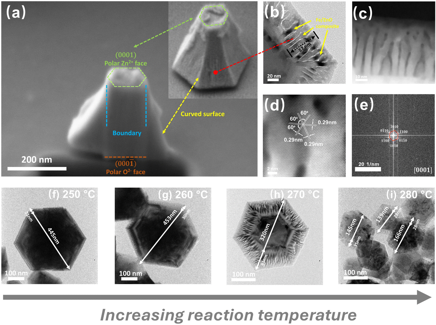
Temperature driven variations in growth of hand-shaped Fe/ZnO nanostructures. In-depth mechanism studies of temperature effects on growth are well explored; Fig. 2f–i show TEM images illustrating the shape evolution at various target temperatures while maintaining the same reaction time. In Fig. 2f, where the reaction temperature is 250 °C, the underneath palm part is hexagonal ZnO dominated, formed through small platelet-like nanoparticle self-assembly, finally evolving into hexagonal palm ZnO. At this stage, the fingers have not fully grown, or are just beginning to grow, showing only short lengths. As the temperature increases (ex. 260 °C and 270 °C), the fingers continue to grow along the c-axis. Due to breaking the morphological symmetry of the nanostructures, the Fe/ZnO hand-shaped structure begins to flip-over, causing a change to a “face-down” configuration. Interestingly, when the temperature reaches 280 °C, the entire nanostructure flips over again, leading to an “edge-up” configuration. This allows for easy observation of the cross-section of both the finger and palm parts. Notably, as observed at reaction temperatures of 260 °C, 270 °C and 280 °C, fingers were growing toward all six equivalent facets of ZnO.27 To elucidate the effects of temperature on the morphology (Fig. 2f–i, S7 and Table S1†), we measured the length of the palm and the diameter of the fingers in each samples. This reveals that the diameter of the finger continued growing, and the palm size also increased with increasing final temperature. Specifically, from 260 °C to 270 °C, the palm size increased by 50%, while the finger diameter nearly doubled. However, from 270 °C to 280 °C, the size increase was only around 15%. This indicates that the lateral growth rate starts to slow down at 270 °C, approaching a stable stage of growth. Therefore, the reaction temperature significantly impacts the growth patterns and morphological symmetry of the nanostructures. By controlling the temperature, we can adjust the size and shape of these nanostructures, thereby tuning their properties for targeted applications.28–33
Precursor concentration effects on hand-shaped Fe/ZnO nanostructures. To test scalability, we doubled (Fig. S10a†) and tripled (Fig. S10b†) the amount of Fe and Zn precursors, as well as ligands, derived from reaction conditions specified in Fig. 2a and S8e,† keeping the solvent volume constant. The scaled-up reaction resulted in Fe/ZnO hand-shaped nanostructures, showing both face-down and edge-up configurations. Compared with Fig. S8e,† the products from the scaled-up reactions exhibit smaller lengths and diameters in the fingers. However, some of the fingers exhibited a hexagonal cross-sectional morphology (circled in red in Fig. S10†). This suggests that hexagonal ZnO forms Fe/ZnO hand-shaped nanostructures through a self-assembly process. In contrast, undoped zinc oxide nanostructures (Fig. S11a†) formed under identical reaction conditions resulted in platelet-like ZnO, indicating that Fe plays a key role in the formation of hand-shaped nanostructures.
0) crystal planes and oriented along the [0001] direction. The higher exposure (brighter) surface was identified as the O-rich surface (000) and the lower exposure surface as Zn-rich surface (0001). The growth process preferred the lower surface energy O-rich surface (000), and formation of metastable amorphous nanostructures contributed to greater disorder on the O-rich crystal plane,27,34 promoting deposition of metal atoms on the O-terminated plane. Similar to the Fe/ZnO hand-shaped nanostructures, Fe atoms played an important role in the formation of the hexagonal nanostructures. As shown in Fig. S11b,† undoped ZnO grew as pyramid-like nanoparticles under the same conditions. However, the introduction of Fe atoms facilitated nanostructure nucleation at the lateral sites through Fe-ligand interactions, forming Fe/ZnO nanostructures, followed by continuous growth along the c-axis to form concave lateral edges (Fig. 3a).
 | ||
| Fig. 3 Morphology characterization of hexagonal Fe/ZnO nanostructures. (a) SEM images of FIB-milled cross-section, with inset showing pre-milled image of the same nanostructure. (b) HRTEM, (c) HAADF-STEM and (d) atomic-resolution HAADF-STEM images of the branch-like edge of a nanostructure, (e) FFT pattern corresponding to (d). TEM images showing the evolution of hexagonal Fe/ZnO nanostructures upon varying the final reaction temperature to values of (f) 250 °C, (g) 260 °C, (h) 270 °C, and (i) 280 °C. | ||
To further explore the surface morphology, SEM stage tilt techniques were employed, Fig. S12b† shows SEM images taken at zero and 36° tilt angles, revealing two additional nanostructures derived from truncated hexagonal pyramids; coupled tail-to-tail nanostructures (circled in blue) and volcano-like nanostructures (circled in purple). The tail-to-tail pyramid coupled nanostructures can be driven by the presence of organic ligands localized on the basal (000) crystal plane. This tail-to-tail assembly may be driven by ligand–ligand interactions as reported for Al-doped ZnO pyramids.35 Tail-to-tail coupled nanostructures were also observed in undoped ZnO (Fig. S11b†), suggesting that the ligands, rather than doping, drive this assembly process. Additionally, in the SEM tilt image (Fig. S12b†) and TEM image (Fig. S13d†), volcano-like nanostructures can also be observed. These images suggest Fe/ZnO nanostructures formed at the lateral edges of the Zn-terminated plane, creating a hat-like top part that gives rise to the volcano-shaped morphology. The surface energy distribution along the c-axis is reflected in the gradient changes of the lateral edges of the nanostructures. Although the Zn-terminated face has a higher surface energy, it exhibits weaker interactions with the species involved in the nucleation and growth process of Fe/ZnO nanostructures. This suggests that nucleation behavior is not only determined by surface energy but also influenced by ligand–ligand interactions on the NC's surface,27,35 leading to preferential growth towards the O-terminated face, where a higher Fe/ZnO composition is adsorbed. However, at some point, the concentration of adsorbed species exceeds a critical threshold, prompting a new burst of growth toward the six symmetric nonpolar (100) planes and producing the hat-like component of the volcano-like morphology.
Temperature driven variations in growth of Fe/ZnO hexagonal nanostructure. Fig. 3f–i shows the shape evolution of these nanostructures as the reaction temperature increased from 250 °C to 280 °C. At 250 °C (Fig. 3f) the outer layer's diagonal measured 21 nm, while the entire nanoparticle's diagonal was 445 nm, so the ratio between outer layer and entire nanoparticle dimension was 0.047. Similar evaluations were performed in Fig. 3f–i. Table S2† summarizes the ratios for nanoparticles synthesized at different temperatures, showing an increase in this ratio from 250 °C to 270 °C and slight decrease at 280 °C. These results suggest an increase in the outer-layer to core growth rate ratio up to the targeted reaction temperature around 270 °C. Based on SEM (Fig. S12†) and TEM images (Fig. 3f–i), the formation mechanism can be divided into two stages; initial hexagonal ZnO formation at lower temperature, followed by temperature-driven growth beginning at the polar O-rich crystal plane and terminating at polar Zn-rich crystal plane, upon further increasing the temperature. The two-step formation mechanisms are consistent with the previous discussion, suggesting different processes govern the formation of the inner core and the lateral branches.
Ligand-driven variations in growth of hexagonal Fe/ZnO nanostructures. FTIR spectra (Fig. S9†), showed the presence of OAm on the product nanostructures. Thus, in this synthesis, it served dual roles: it facilitated the dissolution of metal precursors and acted as a surfactant during the reaction. Meanwhile, myristic acid significantly affected the growth mechanism, even though used in small quantities. In the absence of MA, hexagonal ZnO platelets formed (Fig. S13a†). However, small amounts of MA (Fig. S13b†) significantly promoted the formation of hexagonal Fe/ZnO nanostructures, with a smaller lateral edge-to-core ratio. As MA concentrations increased to 0.66 mmol (Fig. S13c†), metastable lateral edges grew considerably, and at 0.88 mmol (Fig. S13d†), the nanoparticles change to a face-down configuration with clear volcano-like nanostructures.
Based on the above analysis, Fig. 4 schematically illustrates the detailed formation mechanisms we propose for the overall nucleation-growth processes of these Fe-doped ZnO structures; initially, iron acetylacetone and zinc acetate decomposed to form monomers, followed by the incorporation of Fe atoms into the ZnO crystal lattice, forming hexagonal ZnO layers. Subsequently, “fingers” emerged during growth and continued extending along the c-axis as the temperature increased. Specifically, the asymmetric growth of the hand-shaped nanostructures suggests that Fe-doped-ZnO primarily grows along the c-axis, beginning from the O-rich polar surface in the presence of Fe atoms. The low-index O-rich surface (000) exhibits smaller surface energy compared to the Zn-rich surface, which leads to higher disorder.34,36 After several layers of hexagonal ZnO form, individual “fingers” start growing independently, rather than the structure continuing to grow as a single entity. However, using OAm instead of ODE as solvent leads to distinctly different nanostructures with different growth mechanisms. The dissolved precursors form typical ZnO hexagonal prisms along the c-axis at the O-rich polar surface. Subsequently, excess metal ions accumulate near the O-rich polar surface, forming metastable Fe/ZnO nanostructures on the outer surface. The concave lateral edges reflect a gradient change in surface energy distribution across the six equivalent facets of ZnO. Ultimately, the growth process concludes at the lower-energy Zn-rich polar plane.
 | ||
| Fig. 4 Reaction mechanisms of colloidal synthesis of hand-shaped and hexagonal iron-doped-zinc oxide nanostructures. | ||
Optical properties of Fe/ZnO nanostructures
These Fe-doped ZnO nanostructures exhibited variations in optical properties, particularly in relation to their structural properties. Fig. 5a, b, S14 and S15† present a comprehensive study of their UV-vis absorbance spectra. In Fig. 5a and b, both Fe/ZnO nanostructures show a blue shift due to the modulation of their electronic structure, attributed to Fe atoms incorporating into the ZnO lattice,37 resulting in the absorbance peak at 367 nm. The platelet-like undoped ZnO, associated with the hand-shaped structures (Fig. S11a†), has an absorption peak at a shorter wavelength of 370 nm (Fig. 5a), compared to undoped pyramid-like ZnO with an absorbance peak at 378 nm (Fig. 5b), associated with the Fe/ZnO hexagonal structures (Fig. S11b†). The difference may be associated with the size of these nanostructures; the platelet-like ZnO was much smaller in size. A decrease the ZnO size leads to higher effective band gap.38,39 In-depth optical analysis is presented in Fig. S14 and S15,† illustrating UV-vis absorbance change with respect to synthesis temperature and ligand variations in these Fe/ZnO nanostructures. Fig. S14a† shows a blue shift for the hand-shaped nanostructures with increasing temperature, likely due to higher Fe doping. Conversely, Fig. S14b† shows a red shift with increasing temperature; potentially due to the presence of an outer metastable branch-like structure that introduces more oxygen vacancies, leading to red shift.40 In the ligand-modified samples (Fig. S14b, c and S15b†), there is a sharp peak-shifting between samples with and without ligands, indicating that ligands assist in nucleation and growth, creating oxygen vacancies or defects and introducing iron, which contributes to the signal differences. The broader absorbance peaks observed among these samples suggest lower crystallinity, implying that both ligands and Fe assist the formation of high purity nanocrystals. Modifying the ligand concentration in the Fe/ZnO system further shifts the absorbance peaks to longer wavelengths, similar to the effect of increasing temperature in hexagonal Fe/ZnO. | ||
| Fig. 5 Optical properties of Fe/ZnO nanostructures. Normalized UV-vis absorbance spectra of (a) hand-shaped Fe/ZnO and corresponding undoped ZnO and (b) hexagonal Fe/ZnO and corresponding undoped ZnO. Normalized photoluminescence (PL) spectra of (c) hand-shaped Fe/ZnO and corresponding undoped ZnO and (d) hexagonal Fe/ZnO and corresponding undoped ZnO with an excitation wavelength of 340 nm. Undoped ZnO in panels (a) and (c) was synthesized under the conditions used for hand-shaped Fe/ZnO, while undoped ZnO in panels (b) and (d) was synthesized under conditions used for hexagonal Fe/ZnO. | ||
Photoluminescence (PL) is commonly used to evaluate the electronic structure of nanostructures. Fig. 5c and d provide room temperature PL spectra of Fe-doped and undoped ZnO nanostructures. The data show a weak near-band-edge (NBE) emission peak around 380 nm and 391 nm for ZnO, reflecting the energy of electrons transitioning from the conduction band to the valence band.41 However, Fe-doped ZnO nanostructures exhibit a broad peak centered at 417 nm and small onset peak at 471 nm, which could be attributed to defect-related emission caused by Fe doping. Doping of Fe atoms can introduce extra oxygen vacancies VO42 or Zn interstitial defects VZn43 into the ZnO nanostructure. This result is consistent with XPS spectra (Fig. S3 and S5†), which show the presence of VO vacancies. Fig. S16 and S17† illustrate the changes in PL spectra with respect to temperature and ligand changes for these Fe/ZnO nanostructures, showing almost identical patterns to those previously discussed, with some variation attributed to Fe doping levels and surface morphology.44,45
The differences in UV-vis absorption and photoluminescence (PL) spectra for the two types of nanostructures demonstrated the impact of size and shape on optical properties, while the differences between doped and undoped materials include changes caused by both magnetic Fe doping and ligand–ligand interactions leading to shape change. Both structural differences and doping influence defect states and alter the electronic band structure, thereby contributing to the observed optical and magnetic functionalities.
Magnetic properties of Fe/ZnO nanostructures
Bulk magnetization behavior of Fe/ZnO nanostructures was measured at 8 K (Fig. S18a†) and 300 K (Fig. S18b†) under an external magnetic field of up to ±3 T. Typically, ZnO is a diamagnetic material and our Fe/ZnO nanostructures show paramagnetic or superparamagnetic behavior. At low temperatures, the hexagonal Fe/ZnO nanostructures exhibit a higher magnetization of 4 emu g−1 at 3 T, compared to 2.5 emu g−1 for the hand-shaped nanostructures, likely due to higher Fe doping. However, the hand-shaped Fe/ZnO exhibit measurable coercivity (0.025 T) with a sharp transition between superparamagnetic and paramagnetic response at 0.1 T, whereas the hexagonal structures exhibit near-zero coercivity. Fig. S18b† shows results of magnetic measurements conducted at 300 K, showing both Fe/ZnO nanostructures have zero coercivity and the magnetization reaches 0.4 emu g−1 for Fe/ZnO hexagonal nanostructures and 0.33 emu g−1 for hand-shaped Fe/ZnO nanostructures, consistent with the low temperature measurements.Nanostructures of semiconductors doped with magnetic impurities, such as magnetic Fe-doped ZnO, have shown great potential as dilute magnetic semiconductors (DMS) with controllable magnetic anisotropy. Important factors for evaluating the quality of DMS include Curie temperature (Tc), magnetization (M) and magnetic anisotropy, which can be controlled by adjusting the type and concentration of magnetic element doped into the nanostructures. It is critical to understand that intrinsic magnetic anisotropy depends on the presence of n- or p-type lattice defects and magnetic impurities, which are introduced through doping and related to the exposure of polar crystal faces. Encouragingly, our simple one-pot synthesis method for synthesizing Fe/ZnO nanostructures with controllable morphology through ligand–ligand interaction, offers a wide range of impact in various potential applications. The unique Fe-doped ZnO presented in this study represents a significant step toward establishing structure–property relationships in this class of functional materials. Future work will focus on combining computational modeling and experimental synthesis to further elucidate doping mechanisms and surface energy dynamics. This doping strategy can be extended to incorporate other magnetic dopants such as Co and Ni into single-phase wurtzite ZnO, promoting more complex sp–d exchange interactions and resulting magneto-optic functionalities, making them suitable for next-generation magnetic and optoelectronic materials.
Conclusion
In summary, we successfully synthesized two new types of iron-doped, anisotropic hexagonal ZnO nanostructures. Comprehensive structural analysis revealed that the nanocrystal growth process is highly dependent on precise control of ligand–ligand interactions. We discovered the remarkable richness and complexity of two-step growth processes, where modifications in ligand interactions significantly influenced the final structures. The interplay between dopants and ligands can be attributed to the difference in surface energy distribution among specific crystal facets, promoting growth in a preferred direction. Both Fe-doped-zinc oxide nanostructures exhibit a metastable phase that was enhanced by excess ligands and increased temperature, while another portion of the nanostructure tended to stabilize. The observed magnetic and optical properties are attributable to Fe-induced defects as well as the shape anisotropy of the nanostructures. We anticipate that the heterogeneous atom-induced anisotropic growth method can be extended to other nanostructures to synthesize size-tunable binary or even multiple element nanostructures. This approach opens new possibilities for creating materials with flexible features such as uniformly dispersed solute atoms, selectable crystal facet exposure, and high defect density. These advances are promising for applications in optical metamaterials, optoelectronics, and magneto-optical devices. This work also provides motivation to integrate future combinations of computational and experimental studies to explore more complex nanostructures with anisotropic properties.Experimental section
Chemicals and materials
Iron(III) acetylacetonate (Fe(acac)3) 99+%, was purchased from Acros Organcis. Zinc acetate (Zn(OAc)2) 99.99%, oleylamine (OAm) 70% and myristic acid (MA) ≥99% were purchased from Sigma Aldrich. 1-Octadecene (ODE) 90% was purchased from Alfa Aesar.Synthesis of Fe/ZnO hand-shaped nanostructures
The synthesis method followed the general approach previously reported.2,46 In summary, 0.4 mmol of Fe(acac)3, 0.6 mmol of Zn(OAc)2, 62.5 mmol ODE, 3.04 mmol of OAm and 0.44 mmol MA were added a three-neck flask at room temperature then heated to 110 °C under uniform argon flow for 30 min to remove dissolved oxygen. The flask was wrapped with glass wool and sealed to prevent heat loss during further reaction steps. The mixture was heated to 250 °C over approximately 40 min, then slowly heated to 270 °C over approximately 20 min. After reaction was completed, the reaction was stopped by removing the heating manual and allowing the flask to cool to room temperature. The product was collected and washed with toluene and ethanol using centrifugation at 8000 rpm for 10 min. The washing process was repeated 3 times and followed by one-time centrifugation at 3000 rpm for 30 min to remove the excess surfactants and iron oxide. The final collected product was dispersed in toluene for further characterization.Synthesis of Fe/ZnO truncated hexagonal pyramid nanostructures
0.4 mmol of Fe(acac)3, 0.6 mmol of Zn(OAc)2, 20 mL OAm and 0.44 mmol MA were mixed in a three-neck flask. The remaining procedure was identical to that for synthesizing Fe/ZnO hand-shaped structures.Characterization
TEM images were acquired using a JEOL JEM 2010 microscope operated at 200 kV. Scanning transmission electron microscopy (STEM) and energy dispersive X-ray spectroscopy (EDS) characterization were conducted using a Thermo Fisher Scientific Talos F200X G2 S/TEM equipped with a Super-X detector and operating at 200 kV. EDS data was collected with a 6 second frame time, 20 microsecond dwell time, for a total of 3 minutes for hand-shaped nanostructures and 5 minutes for hexagonal nanostructures. SEM images were acquired using a Carl Zeiss Auriga crossbeam focused ion beam scanning electron microscope (FIB-SEM). The elemental analysis was obtained by energy dispersive X-ray spectroscopy (EDS) (Oxford Instruments, X-Max 20 mm2) in the SEM. Fourier-transform infrared (FTIR) spectra were obtained using a Spectrum II FTIR spectrophotometer (PerkinElmer, Waltham, MA, USA). Ultraviolet-visible spectra (UV-vis) were measured with a UV-vis NIR scanning spectrophotometer (Shimadzu). Room temperature PL studies were carried out using a Shimadzu spectrofluorophotometer (RF – 5301 PC). Magnetic hysteresis loops were obtained using Physical Property Measurement System (PPMS) – Quantum Design Evercool II with vibrating sample magnetometer (VSM). Powder XRD patterns were acquired using a Rigaku Ultima IV with Cu Kα X-ray source. X-ray photoelectron spectroscopy data was employed to analyze the surface metal valence of active sites (Thermo Fisher, USA). The photoelectron spectrometer system was equipped with an Al Kα excitation source with a spot size of 400 μm.Data availability
Data supporting the results presented here are provided in the manuscript and ESI.† Additional data, or data in other formats, is available from the corresponding authors upon reasonable request.Author contributions
Z. X., C. D. and M. T. S. conceived the ideas and the experiments. Z. X. performed the materials synthesis. A. D., S. L., Y. Q., K. C. and Z. F. performed the material characterizations. P. N. P. provided resources. Z. X. wrote the initial draft of the manuscript. C. D. and M. T. S. revised the manuscript. C. D., P. N. P. and M. T. S. jointly supervised this work. All authors provided input and agreed to the final form of the manuscript.Conflicts of interest
There are no conflicts to declare.Acknowledgements
The authors acknowledge support from the Air Force Office of Scientific Research (Program Officer: Dr. Brett Pokines), Grant # FA9550-20-1-0428. The authors also acknowledge support from Thermo Fisher Scientific (Research Scientist: Joseph Cline), for STEM and STEM-EDS imaging. The work at the Molecular Foundry was supported by the Office of Science, Office of Basic Energy Sciences, of the U.S. Department of Energy under Contract # DE-AC02-05CH11231.References
- L. Qiao, Z. Fu, J. Li, J. Ghosen, M. Zeng, J. Stebbins, P. N. Prasad and M. T. Swihart, ACS Nano, 2017, 11, 6370–6381 Search PubMed.
- Z. Fu, Z. Xuan, C. Li, L. Qiao, Y. Liu and M. T. Swihart, ACS Appl. Nano Mater., 2021, 4, 995–999 Search PubMed.
- A. Pan, B. He, X. Fan, Z. Liu, J. J. Urban, A. P. Alivisatos, L. He and Y. Liu, ACS Nano, 2016, 10, 7943–7954 CrossRef CAS PubMed.
- H. J. Kwon, K. Shin, M. Soh, H. Chang, J. Kim, J. Lee, G. Ko, B. H. Kim, D. Kim and T. Hyeon, Adv. Mater., 2018, 30, 1704290 Search PubMed.
- J.-E. Park, Y. Lee and J.-M. Nam, Nano Lett., 2018, 18, 6475–6482 CrossRef PubMed.
- H. F. Greer, W. Zhou, G. Zhang and H. Ménard, Adv. Mater. Interfaces, 2017, 4, 1601238 CrossRef.
- R. Hailili, H. Ji, K. Wang, X. A. Dong, C. Chen, H. Sheng, D. W. Bahnemann and J. Zhao, ACS Catal., 2022, 12, 10004–10017 CrossRef.
- C. Han, Z. Chen, N. Zhang, J. C. Colmenares and Y. J. Xu, Adv. Funct. Mater., 2015, 25, 221–229 CrossRef.
- M.-H. Liu, Y.-W. Chen, T.-S. Lin and C.-Y. Mou, ACS Catal., 2018, 8, 6862–6869 CrossRef.
- S. Chen, A. M. Abdel-Mageed, C. Mochizuki, T. Ishida, T. Murayama, J. Rabeah, M. Parlinska-Wojtan, A. Brückner and R. J. R. Behm, ACS Catal., 2021, 11, 9022–9033 CrossRef.
- F. Liu, X. Lu, C. Zhu, Z. Bian, X. Song, J. Sun, B. Zhang, J. Weng, A. Subramanian and X. Tong, ACS Nano, 2023, 17, 12603–12615 CrossRef.
- Q. Zhang, G. Xie, M. Duan, Y. Liu, Y. Cai, M. Xu, K. Zhao, H. Tai, Y. Jiang and Y. Su, ACS Appl. Nano Mater., 2023, 6, 17445–17456 CrossRef.
- B. S. Jessen, L. Gammelgaard, M. R. Thomsen, D. M. Mackenzie, J. D. Thomsen, J. M. Caridad, E. Duegaard, K. Watanabe, T. Taniguchi and T. J. Booth, Nat. Nanotechnol., 2019, 14, 340–346 CrossRef.
- Y. Yang, J. T. Lee, T. Liyanage and R. Sardar, J. Am. Chem. Soc., 2019, 141, 1526–1536 CrossRef PubMed.
- M. Bürkle, M. Lozac'h, C. McDonald, M. Macias-Montero, B. Alessi, D. Mariotti and V. Švrček, Adv. Funct. Mater., 2020, 30, 1907210 CrossRef.
- X. Zha and A. Travesset, J. Phys. Chem. C, 2018, 122, 23153–23164 CrossRef CAS.
- J. Dehnel, Y. Barak, I. Meir, A. K. Budniak, A. P. Nagvenkar, D. R. Gamelin and E. Lifshitz, ACS Nano, 2020, 14, 13478–13490 CrossRef CAS PubMed.
- P. Wainer, O. Kendall, A. Lamb, S. J. Barrow, A. Tricoli, D. E. Gomez, J. van Embden and E. Della Gaspera, Chem. Mater., 2019, 31, 9604–9613 CrossRef CAS.
- X. Wang, W. Shi, Z. Jin, W. Huang, J. Lin, G. Ma, S. Li and L. Guo, Angew. Chem., Int. Ed., 2017, 129, 9983–9987 CrossRef.
- Y. Luo, L. Niu, Y. Wang, P. Wen, Y. Gong, C. Li and S. Xu, Nanoscale, 2022, 14, 16220–16232 RSC.
- R. Chen, F. Luo, Y. Liu, Y. Song, Y. Dong, S. Wu, J. Cao, F. Yang, A. N'Diaye and P. Shafer, Nat. Commun., 2021, 12, 3952 CrossRef CAS.
- A. G. Roca, I. V. Golosovsky, E. Winkler, A. López-Ortega, M. Estrader, R. D. Zysler, M. D. Baró and J. Nogués, Small, 2018, 14, 1703963 CrossRef.
- N. Ali, B. Singh, V. Ar, S. Lal, C. Yadav, K. Tarafder and S. Ghosh, J. Phys. Chem. C, 2021, 125, 7734–7745 CrossRef.
- Y. Ma, H. Gao, R. Huang, R. Guo, S. Yang, Y. Han and H. Zuo, J. Lumin., 2022, 241, 118521 CrossRef.
- J. He, Y. Liu, Y. Huang, H. Li, Y. Zou, C. L. Dong and S. Wang, Adv. Funct. Mater., 2021, 31, 2009245 CrossRef.
- X. Meng, F. Zhang, H. Guo, C. Zhang, H. Hu, W. Wang, J. Liu, X. Shuai and Z. Cao, Adv. Healthcare Mater., 2021, 10, 2100780 CrossRef CAS.
- S. Theiss, M. Voggel, H. Kuper, M. Hoermann, U. Krings, P. Baum, J. A. Becker, V. Wittmann and S. Polarz, Adv. Funct. Mater., 2021, 31, 2009104 CrossRef CAS.
- X. Liu and M. T. Swihart, Nanoscale, 2013, 5, 8029–8036 RSC.
- X. Li, Y. Liu, J. Song, J. Xu and H. Zeng, Small, 2015, 11, 5097–5104 CrossRef CAS PubMed.
- C. Li, Q. Li, R. Ge and X. Lu, Chem. Eng. J., 2023, 458, 141355 Search PubMed.
- D. Zhou, J. Yuan, Y. Zhou and Y. Liu, Sci. Rep., 2020, 10, 10889 Search PubMed.
- K. Chang, C. Podder and H. Pan, ACS Appl. Nano Mater., 2023, 6, 23418–23429 CrossRef CAS.
- I. A. Safo, C. Dosche and M. Özaslan, ChemPhysChem, 2019, 20, 3010–3023 CrossRef CAS.
- D. Mora-Fonz, T. Lazauskas, M. R. Farrow, C. R. A. Catlow, S. M. Woodley and A. A. Sokol, Chem. Mater., 2017, 29, 5306–5320 CrossRef CAS.
- E. Javon, M. Gaceur, W. Dachraoui, O. Margeat, J. Ackermann, M. I. Saba, P. Delugas, A. Mattoni, S. Bals and G. Van Tendeloo, ACS Nano, 2015, 9, 3685–3694 CrossRef PubMed.
- H. F. Wilson, C. Tang and A. S. Barnard, J. Phys. Chem. C, 2016, 120, 9498–9505 Search PubMed.
- G. Soldan, M. A. Aljuhani, M. S. Bootharaju, L. G. AbdulHalim, M. R. Parida, A. H. Emwas, O. F. Mohammed and O. M. Bakr, Angew. Chem., Int. Ed., 2016, 128, 5843–5847 Search PubMed.
- A. Sulciute, K. Nishimura, E. Gilshtein, F. Cesano, G. Viscardi, A. G. Nasibulin, Y. Ohno and S. Rackauskas, J. Phys. Chem. C, 2021, 125, 1472–1482 Search PubMed.
- B. Clarke and K. Ghandi, Small, 2023, 19, 2302864 Search PubMed.
- H.-L. Guo, Q. Zhu, X.-L. Wu, Y.-F. Jiang, X. Xie and A.-W. Xu, Nanoscale, 2015, 7, 7216–7223 RSC.
- J. Lin, M. Penchev, G. Wang, R. K. Paul, J. Zhong, X. Jing, M. Ozkan and C. S. Ozkan, Small, 2010, 6, 2448–2452 Search PubMed.
- W.-C. Lee, J.-Y. Chen, C.-W. Huang, C.-H. Chiu, T.-Y. Lin and W.-W. Wu, Chem. Mater., 2015, 27, 4216–4221 CrossRef.
- H. Zeng, G. Duan, Y. Li, S. Yang, X. Xu and W. Cai, Adv. Funct. Mater., 2010, 20, 561–572 CrossRef.
- M. Shatnawi, A. Alsmadi, I. Bsoul, B. Salameh, G. Alna'Washi, F. Al-Dweri and F. El Akkad, J. Alloys Compd., 2016, 655, 244–252 CrossRef.
- F. Wang, J. Du, F. Sun, R. F. Sabirianov, N. Al-Aqtash, D. Sengupta, H. Zeng and X. Xu, Nanoscale, 2018, 10, 11028–11033 RSC.
- Z. Fu, L. Qiao, Y. Liu, Z. Xuan, C. Li, S. R. Pillai, C. Lee and M. Swihart, J. Mater. Chem. C, 2020, 8, 14056–14065 Search PubMed.
Footnote |
| † Electronic supplementary information (ESI) available. See DOI: https://doi.org/10.1039/d5sc01974e |
| This journal is © The Royal Society of Chemistry 2025 |