
 Open Access Article
 This Open Access Article is licensed under a Creative Commons Attribution-Non Commercial 3.0 Unported Licence
A general “gas–liquid” synthesis strategy towards centimeter-scale two-dimensional non-layered semiconductors†
Jiahui
Liu‡
a,
Jiangbo
Yuan‡
a,
Hao
Liu‡
a,
Zhiyi
Yuan
a,
Baochuan
Guo
a,
Shaohui
Li
 a,
Qiuhong
Cui
*b,
Qun
Xu
*a and
Cong
Wei
*a
a,
Qiuhong
Cui
*b,
Qun
Xu
*a and
Cong
Wei
*a
aCollege of Materials Science and Engineering, Zhengzhou University, Zhengzhou 450001, China. E-mail: qunxu@zzu.edu.cn; weicong@zzu.edu.cn
bKey Laboratory of Luminescence and Optical Information, Ministry of Education, Beijing Jiaotong University, Beijing, 100044, China. E-mail: qhcui@bjtu.edu.cn
First published on 2nd June 2025
Abstract
Two-dimensional (2D) non-layered semiconductors have attracted tremendous research interest due to their exotic structural and electronic properties compared with their layered counterparts. However, the lack of large-scale growth methods greatly hinders their application. In this work, we have proposed a gas–liquid heterogeneous reaction strategy to suppress the diffusion of the involved reactants, resulting in the anisotropic growth of centimeter-scale 2D non-layered CdS film at the gas–liquid interface. The thickness of the 2D film can be effectively modulated in the range from 10 to 50 nm by adjusting the viscosity of the liquid solvent. A photodetector designed on the CdS film exhibits a high photoswitching (Ilight/Idark) ratio (up to 2 × 10³), high specific detectivity (∼1011 Jones) and excellent stability. Moreover, centimeter-scale 2D ZnS, TiO2, SnO2 and even layered MoS2 were also obtained by designing corresponding reaction systems, illustrating the apparent universality of the “gas–liquid” strategy. Our results pave a novel avenue for the growth of wafer-scale 2D materials, especially non-layered ones, which will foster their potential applications in integrated optoelectronics.
1 Introduction
2D semiconductors, with thickness-dependent bandgaps,1–3 quantum confinement effects,4 enhanced electron–hole interaction strength5 and effective valley polarization,6,7 have been considered as the best candidates for next-generation electronic and optoelectronic devices.8–15 Layered materials, such as graphite or transition-metal dichalcogenides, are held together by van der Waals interactions and can be easily exfoliated into 2D planar structures through mechanical shearing,16 ion intercalation,17,18 layer-resolved splitting techniques19 and so on. However, most semiconductors, especially the common III–V and II–VI species, are non-layered structures.20 The inherent strong covalent bonding in three dimensions makes them more difficult to exfoliate into 2D sheets than their layered counterparts.21 Moreover, when their thickness is reduced to the atomic scale, abundant exposed dangling bonds and unsaturated atoms will cause a dramatic increase in their surface energy,22–24 which hinders their 2D anisotropic growth. The key to the synthesis of 2D non-layered materials lies in achieving a driving force that fosters competition between lateral and vertical growth.25–29 Currently available strategies use soft or hard templates, such as surfactant monolayers,30–32 lamellar intermediates,33–35 2D sacrificial templates36,37 or layered-structure precursors,38,39 and confined spaces,40–42 to direct the 2D anisotropic growth of non-layered crystals. Nevertheless, these templates are only applicable in some specific scenarios and a generic template is still lacking.In common homogeneous reaction systems, all involved precursors are well mixed and can migrate freely in three dimensions. The morphology of the products is primarily determined by the crystal surface energy.43 Crystal growth rates in directions perpendicular to high-index planes with high surface energy are typically much faster than those along the normal directions of low-index planes.44 Consequently, high-index planes are rapidly eliminated, generally resulting in the formation of three-dimensional nanocrystals.45,46 Alternatively, in heterogeneous reactions, mass diffusion perpendicular to the biphase interface is severely suppressed. Initial products always prefer to grow along the contact boundary of the involved reactants and the biphase interface would be a natural 2D template for synthesizing ultrathin non-layered materials.47–49 The practicability of these templates has been validated in our previous works.50,51 Various ultrathin non-layered nanosheets, such as orthorhombic Bi2S3, monoclinic MoO2, monoclinic CuO, anatase TiO2 and cubic Al2O3, have been successfully synthesized by designing appropriate solid–solid heterogeneous reaction systems. Unfortunately, solid–solid interfacial templates are normally only continuous over a few hundred nanometers. The lateral size of the obtained 2D non-layered materials is inevitably limited to less than one micrometer, which cannot satisfy instrumentation and integration requirements.52–55 Conversely, the gas–liquid interface is theoretically flat and continuous on an infinite scale,56,57 making it a promising heterogeneous system for the synthesis of wafer-scale 2D semiconductors.
In this work, we have designed a gas–liquid heterogeneous reaction system to trigger the 2D anisotropic growth of a non-layered CdS semiconductor. Centimeter-scale free-standing polycrystalline CdS film, with an average thickness of about 16 nm, was successfully synthesized at the gas–liquid interphase boundary. The thickness of the 2D film can be well controlled in the range from 10 to 50 nm by modulating the viscosity of the liquid precursors. Photodetector arrays were prepared to evaluate the instrumentation and integration potential of the as-grown CdS film.58–60 A photodetector designed with 2D non-layered CdS film exhibited a high photoswitching ratio (up to 2 × 10³), high specific detectivity (∼1011 Jones) and excellent stability. In addition, we further extended this gas–liquid synthesis strategy to the growth of 2D non-layered ZnS, TiO2, SnO2 and layered MoS2 films. Centimeter-scale ultrathin films were formed at the interfaces, verifying the universality of the proposed strategy. We anticipate our findings will bring forth inspiration regarding wafer-scale growth techniques for 2D materials, particularly for non-layered semiconductors.
2 Results and discussion
2.1 Growth mechanism and characterization of CdS films
In a typical gas–liquid heterogeneous reaction, the gaseous reactants always start with a condensation transition from the gas to the liquid phase,61 where they can undergo subsequent chemical conversion.62 Gas-to-liquid condensation is generally an exothermic process (ΔH < 0), but is always accompanied by a dramatic entropy decrease (ΔS < 0). Thus, this condensation transition will be severely suppressed at high temperatures (ΔG = ΔH − TΔS > 0) and the liquid surface will become an overwhelming barrier to the entrance of gaseous reactants (Fig. 1a). However, when a liquid precursor is involved, the additional reaction enthalpy can compensate for the entropy decrease and induce the condensation of the gaseous reactants (Fig. 1c). The condensation process will be accompanied by the corresponding chemical reaction, primarily occurring at the gas–liquid interface. Once the reaction rate is much faster than the mass diffusion rate in the liquid phase, the reaction will be restricted within a thin layer on the liquid surface, driving the 2D anisotropic growth. We chose CdS, a well-known non-layered semiconductor, as the model target to verify the feasibility of the proposed gas–liquid synthesis strategy. | ||
| Fig. 1 The mass diffusion barrier in a gas–liquid reaction. Schematic diagrams showing the interfacial capture of gas reactants with (c) and without (a) an added liquid precursor. Photographs (bottom) and optical microscope images (top) of the thiourea-steam-treated starch/glycerin solution with (d) and without (b) added CdCl2. | ||
The gas–liquid heterogeneous reaction was carried out in a tube furnace (Fig. S1†). N2 was used as the carrier gas. An aluminium oxide boat containing thiourea powder was placed in the center of the tube at 180 °C (above the decomposition temperature of thiourea, Fig. S2†) to produce gaseous sulfur. CdCl2/starch/glycerin solution was placed downstream of the tube furnace at 80 °C, acting as a stable liquid precursor with specific viscosity (Fig. S3†). The starch was used to increase the viscosity of the solution, resulting in sluggish mass diffusion in the liquid phase. After thermal treatment for 2 h, a yellow CdS membrane was obtained on the solution surface (Fig. 1d), indicating the successful capture of the gaseous sulfur. However, no significant sulfureous deposit is observed in the blank solution without CdCl2 (Fig. 1b), consistent with the standard methylene blue spectrophotometric method results (Fig. S4†). This proves the validity of our proposed gas–liquid heterogeneous reaction model.
As shown in Fig. 1d, the as-formed CdS film floats on the liquid surface, enabling effortless conformal transfer of the 2D film to various substrates (Fig. 2a, S5 and S6†). Fig. 2a shows a typical CdS film on a glass substrate with a lateral size in the centimeter range. In the corresponding optical microscopy (OM) and scanning electron microscope (SEM) images (Fig. 2b and c), the CdS films show homogeneous contrast with the substrate, indicating the uniform thickness of the synthesized 2D CdS film. To further confirm the 2D morphology and structure of the obtained CdS film, we performed transmission electron microscope (TEM), high-resolution transmission electron microscope (HRTEM), selected area electron diffraction (SAED) and X-ray diffraction (XRD) measurements. Low-magnification TEM images (Fig. 2d, and S7†) exhibit a nearly transparent appearance with low contrast, demonstrating the ultrathin nature of the as-prepared CdS film. The discontinuous and chaotically arranged lattice fringes in the HRTEM image reveal the polycrystalline nature of the CdS film (Fig. 2e), and lattice fringes with planar spacings of 0.326 nm and 0.197 nm were observed, consistent with the SAED observations (Fig. 2f). The XRD pattern exhibits three weak diffraction peaks, which can be unambiguously indexed to the (010), (002), and (011) crystallographic planes of non-layered hexagonal CdS (PDF# 41-1049, Fig. 2h). This is consistent with the SAED and HRTEM results (Fig. 2e and f). The observed broadened XRD peaks indicated a relatively low degree of crystallinity (Fig. 2g). This phenomenon was attributed to the kinetically controlled synthesis conditions at a low reaction temperature (80 °C). Under this low-temperature regime, atomic diffusion and rearrangement were significantly restricted, leading to the formation of nanoscale crystalline domains (Fig. 2e). Film thickness calibration was accomplished by atomic force microscopy (AFM) measurements. The obtained CdS film was about 16 nm in height with a uniform and smooth surface (Fig. 2i).
 | ||
| Fig. 2 Morphological and structural characterization of the CdS film. (a) A photograph of the centimeter-scale CdS film transferred onto a glass substrate. (b and c) Optical and SEM images of the CdS film. Low-magnification TEM (d) and HRTEM (e) images of the CdS film. (f) The SAED pattern of the obtained CdS film. (g) An XRD image of the CdS film. (h) The crystal structure of the CdS film; the yellow and green balls represent S and Cd atoms, respectively. (i) An AFM image of the CdS film. | ||
Energy-dispersive X-ray spectroscopy (EDS) and X-ray photoelectron spectroscopy (XPS) measurements were employed to identify the elemental composition and atom coordination of the obtained film. The mapping images confirm that Cd and S elements are uniformly distributed over the entire film (Fig. 3a–c). The Cd/S molar ratio was approximately 1![[thin space (1/6-em)]](https://www.rsc.org/images/entities/char_2009.gif) :1 based on the corresponding EDS spectrum (Fig. S8†), aligning with the stoichiometric ratio of CdS crystals. The Cd 3d XPS spectrum of the 2D film exhibits two characteristic peaks at 405.2 eV and 411.8 eV (Fig. 3d), which correspond to the 3d5/2 and 3d3/2 orbital electrons of Cd2+, respectively. In addition, the two prominent peaks at 162.7 eV and 161.5 eV in the S 2p spectrum are assigned to the S 2p1/2 and S 2p3/2 orbitals of S2− (Fig. 3e). These values match well with the general fingerprint of the bulk CdS sample. However, the S 2p spectrum of 2D CdS film also contains an additional broad peak located at 168.7 eV, which is attributed to the formation of S–O bonds.63 These might arise from the numerous surface dangling bonds present in non-layered two-dimensional CdS films that serve as chemical adsorption sites for oxygen species. Subsequently, we retrieved CdS films from different directions to alter the exposed surfaces and compared the chemical states of their top and bottom surfaces. Both surfaces maintain identical Cd2+ and S2− coordination. However, the bottom surface of the CdS film contains a higher density of S–O bonds, which might result from the hydroxyl-rich environment of the glycerol/starch liquid precursor (Fig. S9a–c†). The Raman spectrum of CdS film shows two peaks at frequencies of approximately 297.1 and 595.5 cm−1 (Fig. 3f), corresponding to the first-order and second-order longitudinal optical (LO) modes. Compared with the bulk sample, the LO signals of the 2D film exhibit a significant red shift (∼10 cm−1) along with broadening effects, which result from an attenuation in oscillator strength associated with Cd–S bonds induced by the ultrathin thickness.
:1 based on the corresponding EDS spectrum (Fig. S8†), aligning with the stoichiometric ratio of CdS crystals. The Cd 3d XPS spectrum of the 2D film exhibits two characteristic peaks at 405.2 eV and 411.8 eV (Fig. 3d), which correspond to the 3d5/2 and 3d3/2 orbital electrons of Cd2+, respectively. In addition, the two prominent peaks at 162.7 eV and 161.5 eV in the S 2p spectrum are assigned to the S 2p1/2 and S 2p3/2 orbitals of S2− (Fig. 3e). These values match well with the general fingerprint of the bulk CdS sample. However, the S 2p spectrum of 2D CdS film also contains an additional broad peak located at 168.7 eV, which is attributed to the formation of S–O bonds.63 These might arise from the numerous surface dangling bonds present in non-layered two-dimensional CdS films that serve as chemical adsorption sites for oxygen species. Subsequently, we retrieved CdS films from different directions to alter the exposed surfaces and compared the chemical states of their top and bottom surfaces. Both surfaces maintain identical Cd2+ and S2− coordination. However, the bottom surface of the CdS film contains a higher density of S–O bonds, which might result from the hydroxyl-rich environment of the glycerol/starch liquid precursor (Fig. S9a–c†). The Raman spectrum of CdS film shows two peaks at frequencies of approximately 297.1 and 595.5 cm−1 (Fig. 3f), corresponding to the first-order and second-order longitudinal optical (LO) modes. Compared with the bulk sample, the LO signals of the 2D film exhibit a significant red shift (∼10 cm−1) along with broadening effects, which result from an attenuation in oscillator strength associated with Cd–S bonds induced by the ultrathin thickness.
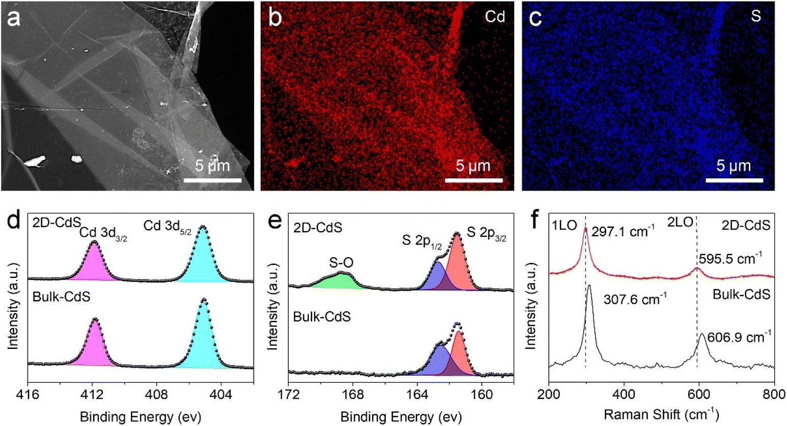 | ||
| Fig. 3 EDS and XPS characterization of the CdS film. (a–c) An STEM image and EDS elemental mapping of Cd and S for the as-prepared CdS film. (d and e) Cd 3d and S 2p XPS spectra for the 2D CdS film and bulk CdS. (f) Raman spectra of the 2D CdS film and bulk CdS. | ||
The intermediates at the gas–liquid interface were collected after different reaction times to investigate the formation mechanism of the CdS film. OM images in Fig. 4a–d and the provided schematic diagram (Fig. 4e), illustrate the structural evolution of the film. As shown in Fig. 4a, the gas–liquid interface is flat and continuous over the entire field of view, and it is an ideal heterogeneous template to direct 2D anisotropic growth on a large scale. In the initial stage, separated 2D CdS flakes formed on the liquid surface (Fig. 4b). These isolated flakes then laterally grew along the gas–liquid interface and gradually merged into a continuous film (Fig. 4c). This evolution process indicated that the vertical growth of CdS was severely suppressed and that chemical conversion was restricted within a thin layer on the liquid surface, highly consistent with the proposed gas–liquid heterogeneous reaction model illustrated in Fig. 1. The formed 2D film floated on the liquid surface, which would hinder the subsequent meeting of the gas and liquid precursors. Thus, the heterogeneous interfacial reaction was spontaneously terminated and a complete CdS film was obtained on the liquid surface (Fig. 4d). The lateral size of the as-prepared 2D film is solely determined by the area of the gas–liquid interface. Theoretically, the infinitely extendable gas–liquid interface would make it possible to synthesize 2D films with an arbitrary lateral size. Fig. S10† presents the morphology of CdS synthesized via a normal solvothermal reaction, in which Cd ions and thiourea were mixed well and homogeneously dispersed in starch/glycerin solution. Clear nanoparticles rather than 2D-shaped nanosheets were obtained, further confirming the key role of the heterogeneous reaction system in the 2D anisotropic growth of CdS film.
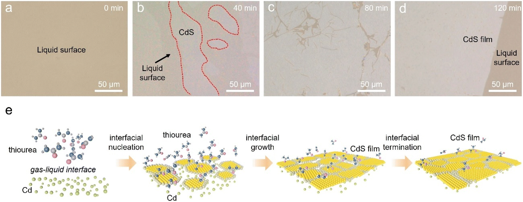 | ||
| Fig. 4 Characterization of the CdS film growth process. Optical images of the interface products after different reaction times: (a) 0 min, (b) 40 min, (c) 80 min, and (d) 120 min. (e) A schematic diagram of the CdS film growth process. | ||
As the physical and chemical properties of a 2D material are strongly dependent on its thickness, it is essential to develop an efficient method for controlling the thickness of 2D CdS film. According to the gas–liquid heterogeneous reaction model illustrated in Fig. 1, the thickness of 2D CdS film was mainly determined by the diffusion depth of the sulfur source. Thicker film would be obtained when the sulfur precursors or intermediates have a longer diffusion distance before being captured (Fig. 5a). Based on the Stokes–Einstein equation, the diffusion coefficient (D) is inversely proportional to the viscosity of the liquid phase, which can be well regulated by adjusting the amount of starch added (Fig. S11†). At 80 °C (the growth temperature for CdS film), the viscosity of the starch/glycerin solution dramatically increased from 0.5 × 10⁴ to 8.9 × 10⁴ mPa s upon increasing the starch/glycerin weight ratio from 0.1 to 0.3 (Fig. 5b). By varying the amount of starch added while keeping the other conditions (e.g., the temperature and concentration of CdCl2) constant, we found that the thickness of the produced CdS film (Fig. 5c–k) shows a systematic response to the increase in liquid viscosity. The average thickness of the obtained CdS film is about 51, 28 and 13 nm when the starch/glycerin weight ratio is 0.1, 0.2 and 0.3, respectively (Fig. S12†).
 | ||
| Fig. 5 Regulation of the thickness of wafer-scale CdS films. (a) A schematic diagram of the gas–liquid reaction under high-viscosity and low-viscosity conditions. (b) A plot of the solution viscosity versus the starch/glycerol ratio at 80 °C. Typical OM, SEM and corresponding AFM images of the CdS films synthesized with different starch/glycerol ratios: (c, f and i) 0.1; (d, g and j) 0.2; and (e, h and k) 0.3. | ||
2.2 Optoelectronic performance of the 2D CdS films
To evaluate the photoelectric performance of the as-grown CdS film, photodetectors were fabricated by thermally depositing Au electrodes on the CdS film using copper mesh as a mask.64,65 The centimeter-scale dimensions of the CdS film enable the simultaneous deposition of nearly a hundred pairs of electrodes, signifying great potential for large-scale device array integration.66 Fig. S13† shows optical images of Au–CdS–Au photodetector arrays on a SiO2/Si substrate. Each device has a width of 25 μm and a length of 58 μm, resulting in an effective illumination area of 1.45 × 10⁻⁵ cm2 (Fig. 6a, inset). The UV-visible absorption spectrum of CdS, shown in Fig. 6b, clearly indicates significant light absorption below 500 nm. As a typical direct-bandgap semiconductor, the band gap (Eg) of CdS can be determined using Tauc's relation: (αhν)2 = k (hν − Eg), where α is the absorption coefficient, h is Planck's constant, ν is the optical frequency, and Eg is the bandgap energy. Based on the extrapolation of the linear intercept shown in the inset of Fig. 6b, the optical bandgap of the prepared CdS film is 2.49 eV, consistent with previous reports.67 Photoluminescence (PL) analysis of 2D CdS film was performed under excitation at 360 nm. A near-band-edge fluorescence emission peak at 538 nm was observed (Fig. S14†), consistent with the band gap value obtained from the UV-vis absorption spectrum (Fig. 6b). Fig. 6c shows the current–voltage (I–V) curves under dark conditions and 400 nm illumination at various light intensities. The photocurrent under dark conditions was very small and enhanced dramatically under light illumination. The corresponding time-dependent photoresponse of the CdS photodetector when the 400 nm light was switched on and off at a bias voltage of 20 V is illustrated in Fig. 6d. The photoswitching on/off ratio (Ilight/Idark) can reach up to 2 × 10³ under 37.2 mW cm−2 illumination. The corresponding responsivity (Rλ) and specific detection rate (D*) are calculated to be 7.97 mA W−1 and 1.19 × 10¹¹ Jones, according to the respective equations Rλ = Iph/PS and D*=(RλS1/2)/(2eIdark)1/2, where Iph (Iph = Ilight − Idark) is the photoexcited current, P is the incident light intensity illuminating the photodetector, S is the effective area, and e is the elementary electronic charge. Fig. 6e plots the relationship of photocurrent versus light intensity, which follows the general power law Iph ∝ Pθ, where θ is an empirical value reflecting the recombination of photoexcited carriers. The fitted value of θ is 0.91, close to the ideal value of 1, suggesting a low recombination ratio of photogenerated carriers in our thin 2D CdS film.68 As shown in Fig. 6f, the 2D CdS photodetector also exhibits excellent stability, with high reproducibility when switching between high and low current states under periodically switched incident light (400 nm, 37.19 mW cm−2).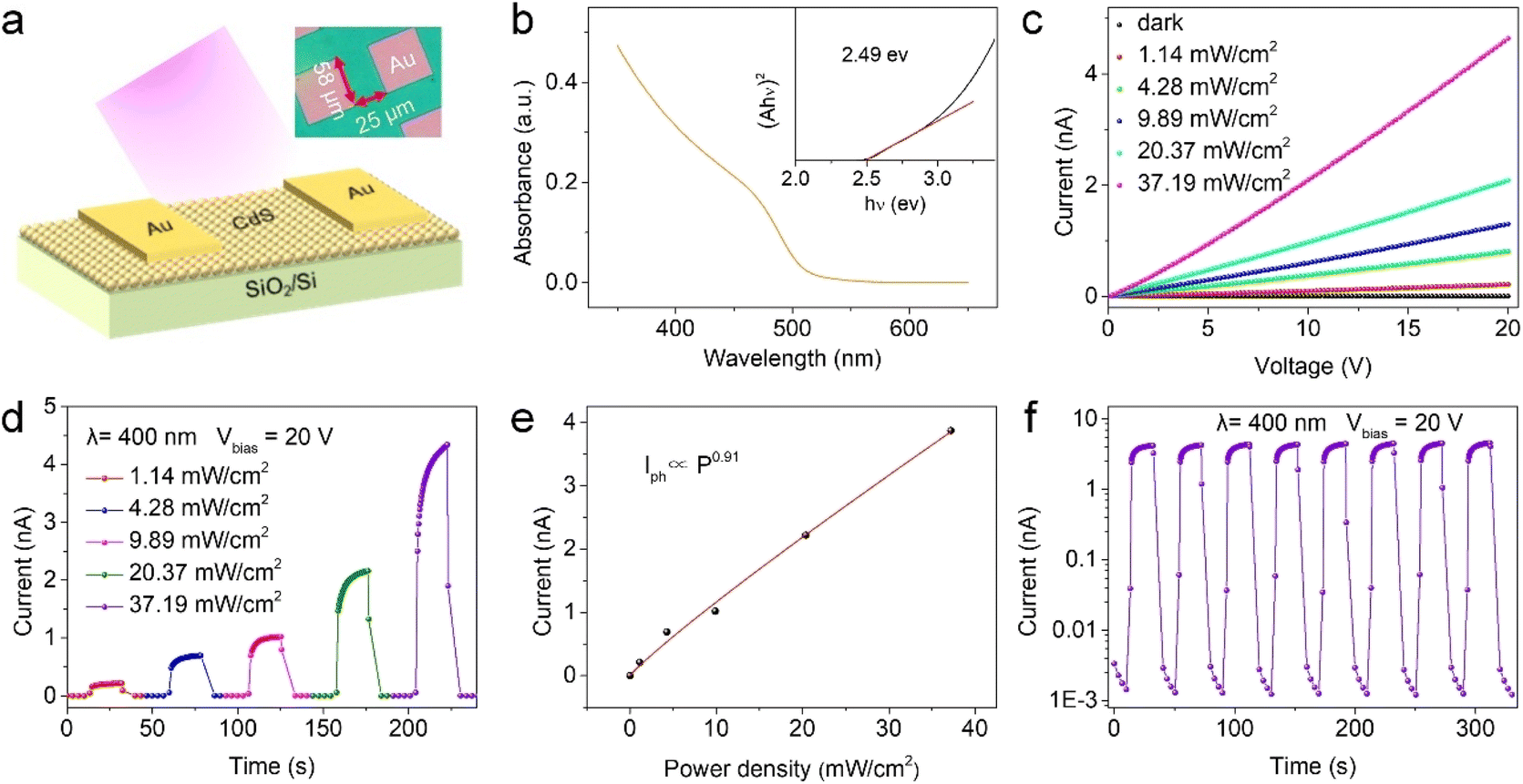 | ||
| Fig. 6 Characterization of the photoelectric properties of 2D CdS films. (a) A schematic diagram of the CdS photodetector. The inset shows a corresponding optical image of an individual CdS photodetector. (b) The UV-vis absorption spectrum of CdS film. The inset shows the corresponding Tauc plot. (c) I–V curves of the CdS photodetector in the dark and in the presence of 400 nm light at different intensities. (d) The time-dependent photoresponse of the CdS photodetector with Vbias = 20 V. (e) The corresponding fitting curve of photocurrent versus incident light intensity using a power law relationship. (f) The photoswitching characteristics of the CdS photodetector in response to 400 nm light (37.19 mW cm−2) illumination with Vbias = 20 V. | ||
2.3 Generality of the “gas–liquid” synthesis strategy
More importantly, our “gas–liquid” strategy is theoretically universal, meaning it can be extended to the synthesis of other 2D materials by designing appropriate reaction systems. Through this strategy, several 2D semiconductors, including non-layered ZnS, TiO2, SnO2 and layered MoS2 (Fig. S15†), have been successfully synthesized (Fig. 7). As shown in Fig. 7a–d, all of the semiconductor films possess 2D morphology with a lateral size up to the centimeter-scale. The obtained films also can be picked up directly from the liquid phase and transferred to different substrates (Fig. S16†), facilitating subsequent device fabrication and integration.69 These films had a homogeneous appearance during optical imaging (Fig. 7e–h), indicating the uniform thicknesses of the synthesized films. The formation of wrinkles and cracks is attributed to the liquid phase transfer process, which might be avoided by optimizing the transfer method.70,71 All the films are highly transparent and barely visible in low-magnification TEM images (Fig. 7i–l and S17a–h†), confirming their 2D ultrathin nature. The HRTEM results indicate that the obtained semiconductor films are predominantly amorphous with only a few nanometer-sized crystalline grains present in the ZnS and MoS2 films (Fig. S17i–l†). The distribution of the involved elements across the films is uniform, as evidenced by EDS mapping images (Fig. S18†). The heights of the films vary based on the chemical composition: around 20 nm for ZnS and 8–10 mm for TiO2, SnO2 and MoS2 (Fig. 7m–p). The successful synthesis of 2D ZnS, TiO2, SnO2 and MoS2 films demonstrates the scalability of the “gas–liquid” heterogeneous reaction, laying the foundation for extending this strategy to the synthesis of other wafer-scale 2D materials. | ||
| Fig. 7 Morphological and structural characterization of the ZnS, TiO2, SnO2 and MoS2 films synthesized via the gas–liquid reaction strategy. Photographs of the obtained (a) ZnS, (b) TiO2, (c) SnO2 and (d) MoS2 films transferred onto SiO2 substrates. Optical images of the (e) ZnS, (f) TiO2, (g) SnO2 and (h) MoS2 films transferred onto SiO2 substrates. Low-magnification TEM images of the (i) ZnS, (j) TiO2, (k) SnO2 and (l) MoS2 films. AFM images of the (m) ZnS, (n) TiO2, (o) SnO2 and (p) MoS2 films. | ||
3 Conclusions
We have proposed a facile “gas–liquid” heterogeneous reaction route to synthesize non-layered 2D CdS film. The gas–liquid interface severely suppresses the diffusion of the involved reactants and drives the 2D anisotropic growth of CdS. Centimeter-scale freestanding 2D polycrystalline CdS film was successfully obtained at the interphase boundary. The thickness of the 2D film was modulated in the range from 10 to 50 nm by adjusting the viscosity of the liquid precursors. A photodetector designed on the 2D non-layered CdS film demonstrates a high photoswitching (Ilight/Idark) ratio (up to 2 × 10³), high specific detectivity (∼1011 Jones) and excellent stability. In addition, our “gas–liquid” strategy is theoretically universal. Centimeter-scale ultrathin 2D non-layered (e.g., ZnS, TiO2 and SnO2) and layered (e.g., MoS2) semiconductor films can also be obtained by selecting appropriate “gas–liquid” reaction systems. We anticipate our “gas–liquid” heterogeneous reaction strategy will open a new avenue to synthesize wafer-scale 2D materials, especially non-layered ones.Data availability
The data supporting this article have been included as part of the ESI.†Author contributions
Q. X. and C. W. conceived and designed the project. Q. C. carried out performance characterization experiments. J. L. and J. Y. carried out all synthesis experiments. J. L., J. Y. and C. W. provided theoretical support for the interpretation of the experimental data. All authors contributed to discussion of the project. J. L., J. Y. and C. W. wrote the manuscript with input from all coauthors.Conflicts of interest
There are no conflicts to declare.Acknowledgements
We are grateful to the National Natural Science Foundation of China (No. 22175154, 21805246, 21773216, and 51173170), China Postdoctoral Science Foundation (No. 2022M712867), the Joint Project from the Henan Provincial, and the China National Natural Science Foundations (Project No. U2004208).References
- C.-T. Toh, H. Zhang, J. Lin, A. S. Mayorov, Y.-P. Wang, C. M. Orofeo, D. B. Ferry, H. Andersen, N. Kakenov, Z. Guo, I. H. Abidi, H. Sims, K. Suenaga, S. T. Pantelides and B. Özyilmaz, Synthesis and properties of free-standing monolayer amorphous carbon, Nature, 2020, 577, 199–203 CrossRef CAS PubMed.
- K. S. Novoselov, A. K. Geim, S. V. Morozov, D. Jiang, Y. Zhang, S. V. Dubonos, I. V. Grigorieva and A. A. Firsov, Electric field effect in atomically thin carbon films, Science, 2004, 306, 666–669 CrossRef CAS PubMed.
- M. Zeng, J. Liu, L. Zhou, R. G. Mendes, Y. Dong, M.-Y. Zhang, Z.-H. Cui, Z. Cai, Z. Zhang, D. Zhu, T. Yang, X. Li, J. Wang, L. Zhao, G. Chen, H. Jiang, M. H. Rümmeli, H. Zhou and L. Fu, Bandgap tuning of two-dimensional materials by sphere diameter engineering, Nat. Mater., 2020, 19, 528–533 CrossRef CAS.
- T. Han, Z. Lu, Y. Yao, J. Yang, J. Seo, C. Yoon, K. Watanabe, T. Taniguchi, L. Fu, F. Zhang and L. Ju, Large quantum anomalous Hall effect in spin-orbit proximitized rhombohedral graphene, Science, 2024, 384, 647–651 CrossRef CAS.
- Z. Wang, D. A. Rhodes, K. Watanabe, T. Taniguchi, J. C. Hone, J. Shan and K. F. Mak, Evidence of high-temperature exciton condensation in two-dimensional atomic double layers, Nature, 2019, 574, 76–80 CrossRef CAS.
- J. R. Schaibley, H. Yu, G. Clark, P. Rivera, J. S. Ross, K. L. Seyler, W. Yao and X. Xu, Valleytronics in 2D materials, Nat. Rev. Mater., 2016, 1, 16055 CrossRef CAS.
- K. F. Mak, K. He, J. Shan and T. F. Heinz, Control of valley polarization in monolayer MoS2 by optical helicity, Nat. Nanotechnol., 2012, 7, 494–498 CrossRef CAS PubMed.
- S. Hwangbo, L. Hu, A. T. Hoang, J. Y. Choi and J.-H. Ahn, Wafer-scale monolithic integration of full-colour micro-LED display using MoS2 transistor, Nat. Nanotechnol., 2022, 17, 500–506 CrossRef CAS.
- M. Kong, M. H. Vong, M. Kwak, I. Lim, Y. Lee, S.-h. Lee, I. You, O. Awartani, J. Kwon, T. J. Shin, U. Jeong and M. D. Dickey, Ambient printing of native oxides for ultrathin transparent flexible circuit boards, Science, 2024, 385, 731–737 CrossRef CAS PubMed.
- Y. Xu, T. Liu, K. Liu, Y. Zhao, L. Liu, P. Li, A. Nie, L. Liu, J. Yu, X. Feng, F. Zhuge, H. Li, X. Wang and T. Zhai, Scalable integration of hybrid high-κ dielectric materials on two-dimensional semiconductors, Nat. Mater., 2023, 22, 1078–1084 CrossRef CAS.
- J. Xue, Y. Dai, S. Wang, J. He, T. Xia, J. Hao, Z. Sofer and Z. Lin, Solution-processable assembly of 2D semiconductor thin films and superlattices with photoluminescent monolayer inks, Chem, 2024, 10, 1471–1484 CAS.
- J. Chen, M. Chen, X. Xin, W. Xin, W. Liu, Y. Bao, M. Ding, P. Li, J. Ma, H. Xu and Y. Liu, Equal-bilayer MoSe2 grown by a nucleation-etching strategy with high carrier mobility, ACS Nano, 2024, 18, 35248–35255 CrossRef CAS.
- K. Yi, W. Qin, Y. Huang, Y. Wu, S. Feng, Q. Fang, X. Cao, Y. Deng, C. Zhu, X. Zou, K.-W. Ang, T. Li, X. Wang, J. Lou, K. Lai, Z. Hu, Z. Zhang, Y. Dong, K. Kalantar-Zadeh and Z. Liu, Integration of high-κ native oxides of gallium for two-dimensional transistors, Nat. Electron., 2024, 7, 1126–1136 CrossRef CAS.
- L. Liu, K. Liu and T. Zhai, Emerging van der Waals Dielectrics of Inorganic Molecular Crystals for 2D Electronics, ACS Nano, 2024, 18, 6733–6739 CrossRef CAS PubMed.
- L. Wen, H. Chen and R. Hao, Wide-field imaging of active site distribution on semiconducting transition metal dichalcogenide nanosheets in electrocatalytic and photoelectrocatalytic processes, Chem. Sci., 2024, 15, 16778–16788 RSC.
- K. R. Paton, E. Varrla, C. Backes, R. J. Smith, U. Khan, A. O'Neill, C. Boland, M. Lotya, O. M. Istrate, P. King, T. Higgins, S. Barwich, P. May, P. Puczkarski, I. Ahmed, M. Moebius, H. Pettersson, E. Long, J. Coelho, S. E. O'Brien, E. K. McGuire, B. M. Sanchez, G. S. Duesberg, N. McEvoy, T. J. Pennycook, C. Downing, A. Crossley, V. Nicolosi and J. N. Coleman, Scalable production of large quantities of defect-free few-layer graphene by shear exfoliation in liquids, Nat. Mater., 2014, 13, 624–630 CrossRef CAS.
- J. Yang, Y. Zhang, Y. Ge, S. Tang, J. Li, H. Zhang, X. Shi, Z. Wang and X. Tian, Interlayer engineering of layered materials for efficient ion separation and storage, Adv. Mater., 2024, 36, 2311141 CrossRef CAS.
- R. Yang, L. Mei, Z. Lin, Y. Fan, J. Lim, J. Guo, Y. Liu, H. S. Shin, D. Voiry, Q. Lu, J. Li and Z. Zeng, Intercalation in 2D materials and in situ studies, Nat. Rev. Chem., 2024, 8, 410–432 CrossRef CAS.
- J. Shim, S.-H. Bae, W. Kong, D. Lee, K. Qiao, D. Nezich, Y. J. Park, R. Zhao, S. Sundaram, X. Li, H. Yeon, C. Choi, H. Kum, R. Yue, G. Zhou, Y. Ou, K. Lee, J. Moodera, X. Zhao, J.-H. Ahn, C. Hinkle, A. Ougazzaden and J. Kim, Controlled crack propagation for atomic precision handling of wafer-scale two-dimensional materials, Science, 2018, 362, 665–670 CrossRef CAS PubMed.
- S. Zhou, R. Wang, J. Han, D. Wang, H. Li, L. Gan and T. Zhai, Ultrathin non-van der waals magnetic rhombohedral Cr2S3: space-confined chemical vapor deposition synthesis and raman scattering investigation, Adv. Funct. Mater., 2019, 29, 1805880 CrossRef.
- Y. Chen, J. Liu, M. Zeng, F. Lu, T. Lv, Y. Chang, H. Lan, B. Wei, R. Sun, J. Gao, Z. Wang and L. Fu, Universal growth of ultra-thin III–V semiconductor single crystals, Nat. Commun., 2020, 11, 3979 CrossRef CAS PubMed.
- A. P. Balan, A. B. Puthirath, S. Roy, G. Costin, E. F. Oliveira, M. A. S. R. Saadi, V. Sreepal, R. Friedrich, P. Serles, A. Biswas, S. A. Iyengar, N. Chakingal, S. Bhattacharyya, S. K. Saju, S. C. Pardo, L. M. Sassi, T. Filleter, A. Krasheninnikov, D. S. Galvao, R. Vajtai, R. R. Nair and P. M. Ajayan, Non-van der waals quasi-2D materials; recent advances in synthesis, emergent properties and applications, Mater. Today, 2022, 58, 164–200 CrossRef CAS.
- L. Lv, W. Dong, D. Li, Q. Liang, P. Wang, C. Zhao, Z. Luo, C. Zhang, X. Huang, S. Zheng, Y. Cui, J. Zhou and Y. Gao, Synthesis of ultrathin FES nanosheets via chemical vapor deposition, Small, 2024, 20, 2402182 CrossRef CAS.
- D. Guo, X.-X. Xue, M. Jiao, J. Liu, T. Wu, X. Ma, D. Lu, R. Zhang, S. Zhang, G. Shao and Z. Zhou, Coordination engineering of single-atom ruthenium in 2D MoS2 for enhanced hydrogen evolution, Chem. Sci., 2024, 15, 16281–16290 RSC.
- Z. Zhao, Z. Fang, X. Han, S. Yang, C. Zhou, Y. Zeng, B. Zhang, W. Li, Z. Wang, Y. Zhang, J. Zhou, J. Zhou, Y. Ye, X. Hou, X. Zhao, S. Gao and Y. Hou, A general thermodynamics-triggered competitive growth model to guide the synthesis of two-dimensional nonlayered materials, Nat. Commun., 2023, 14, 958 CrossRef CAS PubMed.
- J. Zhou, C. Zhu, Y. Zhou, J. Dong, P. Li, Z. Zhang, Z. Wang, Y.-C. Lin, J. Shi, R. Zhang, Y. Zheng, H. Yu, B. Tang, F. Liu, L. Wang, L. Liu, G.-B. Liu, W. Hu, Y. Gao, H. Yang, W. Gao, L. Lu, Y. Wang, K. Suenaga, G. Liu, F. Ding, Y. Yao and Z. Liu, Composition and phase engineering of metal chalcogenides and phosphorous chalcogenides, Nat. Mater., 2023, 22, 450–458 CrossRef CAS PubMed.
- A. Rajan, S. Buchberger, B. Edwards, A. Zivanovic, N. Kushwaha, C. Bigi, Y. Nanao, B. K. Saika, O. R. Armitage, P. Wahl, P. Couture and P. D. C. King, Epitaxial growth of large-area monolayers and van der waals heterostructures of transition-metal chalcogenides via assisted nucleation, Adv. Mater., 2024, 36, 2402254 CrossRef CAS.
- R. Li, Z. Yao, Z. Li, L. Liao, H. Sun, C. Cong, X. Huang, K. Wu, T. Wang, H. Tian, P. Liao, S. Liu, Y. Wang, L. Yang Zhang, U. Sasaki, G. Yin, J. Guo, Y. Ye, X. Wei, X. Wang, J. Hong, J. Mao, L. Bao, L. Wang, X. Bai, P. Gao, K. Liu, L. Liao, J. He, S. Bai, Y. Zhang, Y. Hou, R. Zou, H.-J. Gao, Y. Zhang, E. Wang and L. Liu, Mechanical exfoliation of non-layered metal oxides into ultrathin flakes, Nat. Synth., 2024, 4, 106–115 CrossRef.
- J. Hu, J. Wang, P. Yang, W. Quan, X. Wang, H. Ding, J. Fu, Y. Peng, R. Zhang, H. Wang, L. Xie, K. He, L. Wang, W. Wei, L. Zhang, Z. Liu and Y. Zhang, Low-cost preparation of wafer-scale Au(111) single crystals for the epitaxy of two-dimensional layered materials, ACS Nano, 2025, 19, 4973–4982 CrossRef CAS PubMed.
- X. Hu, P. Huang, B. Jin, X. Zhang, H. Li, X. Zhou and T. Zhai, Halide-Induced self-limited growth of ultrathin nonlayered Ge flakes for high-performance phototransistors, J. Am. Chem. Soc., 2018, 140, 12909–12914 CrossRef CAS.
- Y. Wang, Y. Shi, Z. Zhang, C. Carlos, C. Zhang, K. Bhawnani, J. Li, J. Wang, P. M. Voyles, I. Szlufarska and X. Wang, Bioinspired synthesis of quasi-two-dimensional monocrystalline oxides, Chem. Mater., 2019, 31, 9040–9048 CrossRef CAS.
- E. Yamamoto, D. Kurimoto, K. Ito, K. Hayashi, M. Kobayashi and M. Osada, Solid-state surfactant templating for controlled synthesis of amorphous 2D oxide/oxyhydroxide nanosheets, Nat. Commun., 2024, 15, 6612 CrossRef CAS.
- J. Peng, Y. Liu, H. Lv, Y. Li, Y. Lin, Y. Su, J. Wu, H. Liu, Y. Guo, Z. Zhuo, X. Wu, C. Wu and Y. Xie, Stoichiometric two-dimensional non-van der Waals AgCrS2 with superionic behaviour at room temperature, Nat. Chem., 2021, 13, 1235–1240 CrossRef CAS.
- R. Yang, Y. Fan, L. Mei, H. S. Shin, D. Voiry, Q. Lu, J. Li and Z. Zeng, Synthesis of atomically thin sheets by the intercalation-based exfoliation of layered materials, Nat. Synth., 2023, 2, 101–118 CrossRef CAS.
- H. Ren, X. Xia, Y. Sun, Y. Zhai, Z. Zhang, J. Wu, J. Li and M. Liu, Electrolyte engineering for the mass exfoliation of graphene oxide across wide oxidation degrees, J. Mater. Chem. A, 2024, 12, 23416–23424 RSC.
- Z. Huang, A. Zhou, J. Wu, Y. Chen, X. Lan, H. Bai and L. Li, Bottom-up preparation of ultrathin 2d aluminum oxide nanosheets by duplicating graphene oxide, Adv. Mater., 2016, 28, 1703–1708 CrossRef CAS.
- H. Zhao, Y. Zhu, F. Li, R. Hao, S. Wang and L. Guo, A generalized strategy for the synthesis of large-size ultrathin two-dimensional metal oxide nanosheets, Angew. Chem., Int. Ed., 2017, 56, 8766–8770 CrossRef CAS PubMed.
- L. Najafi, R. Oropesa-Nuñez, S. Bellani, B. Martín-García, L. Pasquale, M. Serri, F. Drago, J. Luxa, Z. Sofer, D. Sedmidubský, R. Brescia, S. Lauciello, M. I. Zappia, D. V. Shinde, L. Manna and F. Bonaccorso, Topochemical transformation of two-dimensional VSe2 into metallic nonlayered VO2 for water splitting reactions in acidic and alkaline media, ACS Nano, 2022, 16, 351–367 CrossRef CAS PubMed.
- M. Zhao, S. Yang, K. Zhang, L. Zhang, P. Chen, S. Yang, Y. Zhao, X. Ding, X. Zu, Y. Li, Y. Zhao, L. Qiao and T. Zhai, A universal atomic substitution conversion strategy towards synthesis of large-size ultrathin nonlayered two-dimensional materials, Nano-Micro Lett., 2021, 13, 165 CrossRef CAS.
- D. Ji, Y. Lee, Y. Nishina, K. Kamiya, R. Daiyan, D. Chu, X. Wen, M. Yoshimura, P. Kumar, D. V. Andreeva, K. S. Novoselov, G.-H. Lee, R. Joshi and T. Foller, Angstrom-confined electrochemical synthesis of sub-unit-cell non-van der waals 2D metal oxides, Adv. Mater., 2023, 35, 2301506 CrossRef CAS.
- K. S. Kim, D. Lee, C. S. Chang, S. Seo, Y. Hu, S. Cha, H. Kim, J. Shin, J.-H. Lee, S. Lee, J. S. Kim, K. H. Kim, J. M. Suh, Y. Meng, B.-I. Park, J.-H. Lee, H.-S. Park, H. S. Kum, M.-H. Jo, G. Y. Yeom, K. Cho, J.-H. Park, S.-H. Bae and J. Kim, Non-epitaxial single-crystal 2D material growth by geometric confinement, Nature, 2023, 614, 88–94 CrossRef CAS PubMed.
- H. Kim and Y. Yoo, Confined fluxes mediate 2D growth, Nat. Synth., 2022, 1, 833–834 CrossRef CAS.
- Q. Chen, Y. Jia, S. Xie and Z. Xie, Well-faceted noble-metal nanocrystals with nonconvex polyhedral shapes, Chem. Soc. Rev., 2016, 45, 3207–3220 RSC.
- B. K. Choi, J. Kim, Z. Luo, J. Kim, J. H. Kim, T. Hyeon, S. Mehraeen, S. Park and J. Park, Shape transformation mechanism of gold nanoplates, ACS Nano, 2023, 17, 2007–2018 CrossRef CAS PubMed.
- M. Chen, B. Wu, J. Yang and N. Zheng, Small adsorbate-assisted shape control of Pd and Pt nanocrystals, Adv. Mater., 2012, 24, 862–879 CrossRef CAS PubMed.
- G. Liu, H. G. Yang, J. Pan, Y. Q. Yang, G. Q. Lu and H.-M. Cheng, Titanium dioxide crystals with tailored facets, Chem. Rev., 2014, 114, 9559–9612 CrossRef CAS PubMed.
- B. Y. Zhang, K. Xu, Q. Yao, A. Jannat, G. Ren, M. R. Field, X. Wen, C. Zhou, A. Zavabeti and J. Z. Ou, Hexagonal metal oxide monolayers derived from the metal–gas interface, Nat. Mater., 2021, 20, 1073–1078 CrossRef CAS PubMed.
- Y. Bai, Y. Xu, L. Sun, Z. Ward, H. Wang, G. Ratnayake, C. Wang, M. Zhao, H. He, J. Gao, M. Wu, S. Lu, G. Bepete, D. Peng, B. Liu, F. Kang, H. Terrones, M. Terrones and Y. Lei, Two-dimensional nanosheets by liquid metal exfoliation, Adv. Mater., 2024, 2416375 Search PubMed.
- H. Jiang, X. Zhang, K. Chen, X. He, Y. Liu, H. Yu, L. Gao, M. Hong, Y. Wang, Z. Zhang and Y. Zhang, Two-dimensional czochralski growth of single-crystal MoS2, Nat. Mater., 2025, 24, 188–196 CrossRef CAS.
- X. Lin, P. Yan, F. Xu, W. Wu, T. Hu, C. Wei and Q. Xu, Solid-phase synthesis of atomically thin two-dimensional non-layered MoO2 nanosheets for surface enhanced Raman spectroscopy, J. Mater. Chem. C, 2019, 7, 7196–7200 RSC.
- W. Qin, H. Liu, J. Liu, J. Yuan, C. Wei and Q. Xu, A heterogeneous reaction strategy towards the general synthesis of 2D non-layered nanomaterials, Mater. Adv., 2022, 3, 4536–4541 RSC.
- A. Zavabeti, A. Jannat, L. Zhong, A. A. Haidry, Z. Yao and J. Z. Ou, Two-dimensional materials in large-areas: synthesis, properties and applications, Nano-Micro Lett., 2020, 12, 66 CrossRef CAS PubMed.
- L. Zhang, J. Dong and F. Ding, Strategies, status, and challenges in wafer scale single crystalline two-dimensional materials synthesis, Chem. Rev., 2021, 121, 6321–6372 CrossRef CAS PubMed.
- W. Zhai, Z. Li, L. Zhai, Y. Yao, S. Li, Y. Wang, Y. Ren, B. Chi, Y. Ge and H. Zhang, Epitaxial growth of wafer-scale single-crystal transition metal dichalcogenide monolayers for future electronics, Matter, 2022, 5, 2405–2408 CrossRef CAS.
- J. Kwon, M. Seol, J. Yoo, H. Ryu, D.-S. Ko, M.-H. Lee, E. K. Lee, M. S. Yoo, G.-H. Lee, H.-J. Shin, J. Kim and K.-E. Byun, 200-mm-wafer-scale integration of polycrystalline molybdenum disulfide transistors, Nat. Electron., 2024, 7, 356–364 CrossRef CAS.
- P. Aukarasereenont, A. Goff, C. K. Nguyen, C. F. McConville, A. Elbourne, A. Zavabeti and T. Daeneke, Liquid metals: an ideal platform for the synthesis of two-dimensional materials, Chem. Soc. Rev., 2022, 51, 1253–1276 RSC.
- Z. Ou, B. Liang, Z. Liang, F. Tan, X. Dong, L. Gong, P. Zhao, H. Wang, Y. Zou, Y. Xia, X. Chen, W. Liu, H. Qi, U. Kaiser and Z. Zheng, Oriented growth of thin films of covalent organic frameworks with large single-crystalline domains on the water surface, J. Am. Chem. Soc., 2022, 144, 3233–3241 CrossRef CAS PubMed.
- X. Zhang, Z. Li, E. Hong, T. Yan and X. Fang, Effective dual cation release in quasi-2D perovskites for ultrafast UV light-powered imaging, Adv. Mater., 2025, 37, 2412014 CrossRef CAS PubMed.
- Y. Hu, X. Zhang, X. Mo, J. Chu, X. Fang and Z. Li, High-purity photoactive α-phase for flexible perovskite photodetectors with modified electron transport layer, Adv. Funct. Mater., 2025, 35, 2412015 CrossRef CAS.
- E. Hong, Z. Li, X. Zhang and X. Fang, Light-state rectification behaviors induced by interlayer excitons in mixed-dimensional single-crystalline perovskite heterostructures, Adv. Funct. Mater., 2025, 35, 2412189 CrossRef CAS.
- A. Sharma and D. White, Effects of gas depletion on gas-liquid reaction systems, Chem. Eng. Sci., 1989, 44, 471–481 CrossRef CAS.
- D. Gómez-Díaz, J. M. Navaza and B. Sanjurjo, Analysis of mass transfer in the precipitation process of calcium carbonate using a gas/liquid reaction, Chem. Eng. J., 2006, 116, 203–209 CrossRef.
- H.-S. Guo, W. Zhao, Q. Ge, N. Jiang, M. Liu and H. Cong, Photoelectrochemical water splitting improved by a cucurbit[7]uril-induced ternary heterojunction, Chem. Eng. J., 2025, 159340, DOI:10.1016/j.cej.2025.159340.
- M. Deng, Z. Li, S. Liu, X. Fang and L. Wu, Wafer-scale integration of two-dimensional perovskite oxides towards motion recognition, Nat. Commun., 2024, 15, 8789 CrossRef CAS.
- E. Hong, Z. Li, X. Zhang, X. Fan and X. Fang, Deterministic fabrication and quantum-well modulation of phase-pure 2D perovskite heterostructures for encrypted light communication, Adv. Mater., 2024, 36, 2400365 CrossRef CAS.
- Z. Li, E. Hong, X. Zhang, M. Deng and X. Fang, Perovskite-type 2D materials for high-performance photodetectors, J. Phys. Chem. Lett., 2022, 13, 1215–1225 CrossRef CAS PubMed.
- L. Que, L. Lu, Y. Xu, X. Xu, M. Zhu, J. Pan, J. Cao, J. Wang, Y. Zheng and C. Li, The Ni2+-LaNiO3/CdS hollow core–shell heterojunction towards enhanced visible light overall water splitting H2 evolution via HER/OER synergism of Ni2+/Ov, Chem. Eng. J., 2023, 469, 143902 CrossRef CAS.
- S.-C. Kung, W. Xing, W. E. van der Veer, F. Yang, K. C. Donavan, M. Cheng, J. C. Hemminger and R. M. Penner, Tunable photoconduction sensitivity and bandwidth for lithographically patterned nanocrystalline cadmium selenide nanowires, ACS Nano, 2011, 5, 7627–7639 CrossRef CAS PubMed.
- C. Hou, S. Zhang, R. Liu, T. Gemming, A. Bachmatiuk, H. Zhao, H. Jia, S. Huang, W. Zhou, J.-B. Xu, J. Pang, M. H. Rümmeli, J. Bi, H. Liu and G. Cuniberti, Boosting flexible electronics with integration of two-dimensional materials, InfoMat, 2024, 6, e12555 CrossRef CAS.
- L. Liu, Z. Cai, S. Xue, H. Huang, S. Chen, S. Gou, Z. Zhang, Y. Guo, Y. Yao, W. Bao and P. Zhou, A mass transfer technology for high-density two-dimensional device integration, Nat. Electron., 2025, 8, 135–146 Search PubMed.
- M. Shang, S. Bu, Z. Hu, Y. Zhao, J. Liao, C. Zheng, W. Liu, Q. Lu, F. Li, H. Wu, Z. Shi, Y. Zhu, Z. Xu, B. Guo, B. Yu, C. Li, X. Zhang, Q. Xie, J. Yin, K. Jia, H. Peng, L. Lin and Z. Liu, Polyacrylonitrile as an efficient transfer medium for wafer-scale transfer of graphene, Adv. Mater., 2024, 36, 2402000 CrossRef CAS PubMed.
Footnotes |
| † Electronic supplementary information (ESI) available. See DOI: https://doi.org/10.1039/d5sc01700a |
| ‡ These authors contributed equally. |
| This journal is © The Royal Society of Chemistry 2025 |