DOI:
10.1039/D5RA06469D
(Paper)
RSC Adv., 2025,
15, 46821-46837
Enhanced photodetectivity and responsivity in In10Se70Te15Bi5 film by time-dependent laser irradiation for photodetector applications
Received
29th August 2025
, Accepted 21st November 2025
First published on 27th November 2025
Abstract
Laser treatment for tuning the thin film properties is regarded as a cost-effective, simple, and environmentally friendly method. The recent work aims at the laser annealing of In10Se70Te15Bi5 film under a 532 nm DPSS laser at variable time scales. The findings from the structural study show an increased dislocation density with reduced crystallite size with irradiation time. The phases like In2Se3 and Bi2Se3 contributed towards the other optical parameters. The reduction in bandgap by 0.023 eV upon laser irradiation shows laser-induced modification in the films. It enhanced the photocurrent, thus increasing the responsivity to 2.52 × 10⁻³ A W−1 and photo detectivity to 6.51 × 10⁸ Jones upon 60 min laser annealing. The particle size reduction is also evident from FESEM images upon laser treatment. The elemental presence is also confirmed from the EDS analysis, along with the XPS core level peaks, which also present the chemical analysis of the films. The laser-induced surface changes affect the surface wettability in terms of a decrease in contact angle, thus increasing the hydrophilicity. The increased refractive index upon laser treatment enhanced the nonlinear values in terms of susceptibility and refractive index. At the same time, the dielectric constant is enhanced by reducing the optical electronegativity through laser illumination. The reduction in transmission resulted in an increased absorbance, which resulted in the enhancement of optical density and reduction in skin depth. The optical quantities, along with the photo response parameters, are useful for visible light photodetectors.
1. Introduction
In recent years, chalcogenide glasses have attracted significant attention from both technological and fundamental research perspectives.1,2 These materials are well-suited for use in optical components, memory discs, infrared fibres, and functional elements of integrated optical systems due to their excellent chemical stability and flexibility. Chalcogenide films undergo thermal relaxation when subjected to rapid temperature changes during quenching, transitioning from a high-enthalpy state to a more stable equilibrium state. Various factors, such as compositional modifications,3,4 annealing processes,5 laser irradiation,6 and ion implantation,7 can significantly influence their bandgap and other optical properties. The electrical and optical behaviours of such thin films continue to be widely explored due to their relevance in advanced technologies.8 Among these, laser-induced modifications in amorphous materials are particularly significant, as they offer deeper insights into the underlying mechanisms of such materials and their practical applications. These photo-induced changes typically involve light irradiation with photon energy close to the bandgap of the amorphous materials. In particular, laser photons with energies near the optical bandgap of the material can trigger localised excitation processes, enhancing optical absorption, modifying surface morphology, and even influencing the refractive index. Selenium-containing chalcogenides are especially advantageous owing to the high crystallisation temperatures, greater mechanical hardness, enhanced photosensitivity, and minimal ageing effects. Recent investigations have revealed that Se-based chalcogenide materials exhibit notable electrical and photoelectrical properties, making them promising candidates for optoelectronic applications.9,10 Although Se has certain limitations, like short lifespan and low sensitivity, it still finds numerous applications. Mixing of other elements such as Te, Ge, In, Sb, and Bi, with Se was done to overcome the shortcomings.11–13 In2Se3 displays multiple crystalline phases at different temperatures, making it suitable for various memory applications with enhanced storage capability.14 The inclusion of Te and Bi to the In–Se matrix not only broadens the compositional flexibility but also alters thermal and optical responses under laser exposure. While tellurium contributes to improved infrared sensitivity and lowers crystallisation temperature, bismuth incorporation can increase stability and modify electronic states. Pandian et al. have reported on indium chalcogenide (In–Te–Se) thin films, highlighting their potential use in volatile phase-change memory (PCM).15 The Bi0.5Na0.5TiO3 films exhibit significant optical nonlinearity along with strong absorption, highlighting their potential for applications in nonlinear photonic devices.16 The In–Se–Te–Bi composite exhibits nonlinear parameters in the 10−10 esu range, which shows an increasing trend in Bi content.17
Laser irradiation has emerged as an effective technique for modifying the microstructure and properties of films in a controlled and localised manner. This facilitates photoinduced structural changes, such as bond rearrangement, partial crystallisation, and defect passivation, leading to significant variations in optical absorption, refractive index, and surface morphology.18,19 Chalcogenide materials exhibit several intriguing properties that make them highly suitable for various optoelectronic applications. Among the most notable photoinduced effects observed in chalcogenide thin films are photodarkening (PD) and photobleaching. These effects are associated with red or blue shifts in the optical absorption edge, resulting in changes to the optical bandgap (Eg).20 The extent of PD and PB largely depends on the material's elemental content and arrangement. For instance, the as-deposited Ge29Sb8Se63 thin film initially exhibited rapid photodarkening (PD), which was later dominated by a slower photobleaching (PB) process. In contrast, the annealed film displayed only PD behaviour even under extended irradiation.21 Laser irradiation of As40Se55Bi5 thin films, using energy equivalent to the material's bandgap, led to structural modifications accompanied by a photodarkening (PD) effect, attributed to changes in defect states within the band structure.22 There is significant variations in optical quantities of As–Se–Sb thin film by laser treatment.23 Moreover, the kinetics of variations associated with the laser-treated film are mostly dependent on the duration of laser annealing. Several studies have also highlighted the optical modifications caused by different durations of gamma irradiation.24 The induced illumination may generate defects within the film, consequently reducing its transmittance.25 The IR motherboard based on Ge–Sb–Se thin film was fabricated using femtosecond laser micromachining, which resulted in a significant decrease in both refractive index and optical bandgap (Eg). It is also accompanied by an increased absorption coefficient at varying laser power.26 The impact of laser treatment influenced morphological, structural, surface wettability, and optical quantities of Bi15In20Se65 films at different time scales. It shows the reduction in optical band gap and enhancement in nonlinear optical properties.12
In our previous work, the study on In10Se70Te20−xBix thin films revealed that the 5% Bi-doped film exhibited a distinct phase transformation behaviour, along with enhanced nonlinear susceptibility as compared to other compositions.17 Previous studies have primarily focused on thermal annealing effects in systems such as In–Se–Bi and In–Se–Te, while laser-induced structural and optical modifications in this specific quaternary composition (In10Se70Te15Bi5) remain unexplored. The present work establishes a direct correlation between laser-induced microstructural reordering, changing morphological, and surface wettability behaviours and optical band gap tuning, accompanied by a reduction in Urbach energy and defect density, subjected to varying exposure durations (0, 5, 10, 30, and 60 minutes). These findings demonstrate that laser irradiation provides a faster and more controllable approach for tailoring the structural, optical, and photodetection properties of chalcogenide thin films, thereby advancing the understanding of photo-induced processes in laser-engineered In–Se–Te–Bi materials.
2. Experimental procedures
2.1. Film deposition and laser illumination procedure
Prior to thin film deposition, bulk sample of In10Se70Te15Bi5 was synthesised via a melt-quenching process. For this, 99.999% purity elemental powders of indium (In), tellurium (Te), bismuth (Bi), and selenium (Se) were accurately weighed in stoichiometric proportions. These were put in a quartz ampoule and then closed through sealing. The sealing was done at 10−3 torr. Next, the ampoule was kept in a programmable furnace, and slowly the heating was raised to 950 °C. It was held for 24 hours for complete mixing of the melt. After quenching and cooling, the resulting bulk ingot was retrieved from the ampoules. The bulk ingot was ground into fine powder, which was subsequently used for thin film coating. The coating of In10Se70Te15Bi5 layer with a thickness of approximately 800 nm was coated over a glass substrate. The thermal evaporation process was adopted for such deposition at 10−5 torr vacuum. The deposition rate was set to 5 Å s−1 for smooth and equal distribution deposition. The thickness measurement was through a thickness monitor, which is inside the Smart Coat 3.0 unit. During the coating process, the substrate was continuously rotated by a motor. The normal temperature conditions were used for the substrate.
For the photodarkening study, a 1 × 1 cm-sized film was cut and placed on the sample holder. The laser light was focused on the film for 0, 5, 10, 30, and 60 minutes. This was done by a 532 nm laser (continuous type) of 58 mW power. After laser irradiation, the irradiated as well as the unirradiated samples were characterised through different experiments (Fig. 1).
 |
| | Fig. 1 Laser treatment schematic diagram. | |
2.2. Characterisation methods
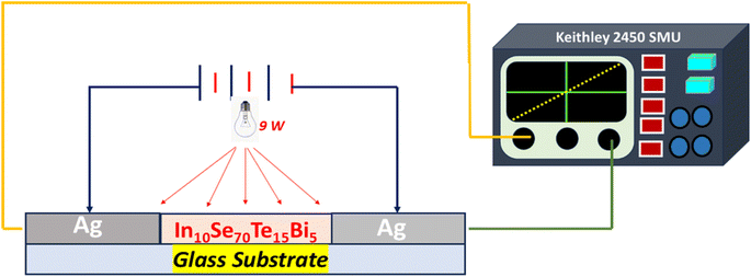
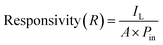
The structural properties of irradiated In10Se70Te15Bi5 films were determined using X-ray diffraction (XRD). The Bruker D8 Advance unit was used for this. For this, the XRD data were collected from 10° to 80° at 0.02° s−1. the instrument was operated at 30 mA current by 40 kV voltage. Field emission scanning electron microscopic (FESEM) images were acquired for the irradiated films at different time scales to notice the surface morphology alteration. Such a picture was captured through the JEOL-JSM-7610F instrument. The operating condition was 9 × 10⁻⁵ torr vacuum at 15 kV voltage. The energy dispersive X-ray analysis (EDS) showed the appearance of corresponding elements in the film before and after laser treatment. The distribution of such elements in the film was visualised by mapping of elements carried out at 11 mA current. The modified surface wettability data of these laser-irradiated films were imaged by a contact angle meter. The pendant water droplet method was employed for taking data. In this method, a 1 µL droplet was allowed to fall onto the film, and the related angle was noted. The average angle was estimated from 3–4 angles at different places. The X-ray photoelectron spectrometer (XPS) was used to perform surface characterization. Axis Ultra, Kratos Analytical instrument with Al Kα as the source (1486.6 eV energy) was used for this. The spectra were collected at 2 × 10⁻⁹ torr. For optical characterization, transmission spectra were taken in a UV-Visible spectrometer (JASCO V-770). The spectra range was within 500–2500 nm, with a spectral resolution of 1 nm. The required optical constants were obtained from the transmittance data using appropriate relations. The photo response of the studied samples was observed by a 2450 Keithley source meter with a 9 W LED bulb. Fig. 2 shows the schematic diagram of the photoresponse measurement setup. The I–V characteristics were recorded by varying the voltage from −10 V to +10 V at a rate of 0.05 V per steps, under both dark and illuminated conditions, using a sample of 5 × 5 mm2 area exposed to incident light.
 |
| | Fig. 2 Photocurrent measurement set-up. | |
3. Results and discussion
3.1. XRD for structural analysis
The XRD data for the laser-irradiated In10Se70Te15Bi5 thin films reveal a polycrystalline nature with distinct diffraction peaks corresponding to In2Se3, Bi2Se3, and elemental Te phases, as shown in Fig. 3(a). In the as-deposited (unirradiated) film, distinct diffraction peaks are observed, indicating that partial crystallization occurs during the deposition process itself, even without laser exposure. Four peaks at 18.42°, 28.15°, 40.45°, and 42.21° refer to In2Se3 rhombohedral phase (ICSD: 01-072-1470). These angles are associated with the (006), (104), (1 010), and (0 0 10) planes. The peak at 23.07° is assigned to hexagonal Te phase (ICDS-00-001-1313). It indicates the (100) plane. Laser-irradiated thin film shows extra peaks at 38.90° corresponding to hexagonal Te phase with plane (1 0 10) and Bi2Se3 rhombohedral phase (ICDS:33-0214) at 41.33° (1 010).
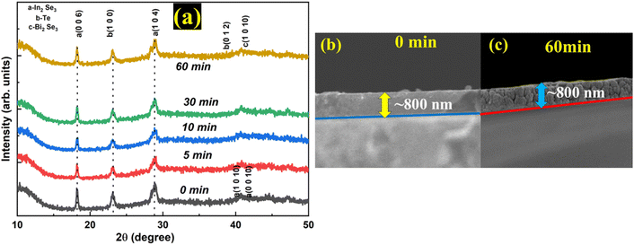 |
| | Fig. 3 (a) XRD patterns, cross-sectional FESEM, (b) 0 min, (c) 60 min irradiated In10Se70 Te15Bi5 thin films. | |
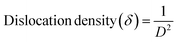
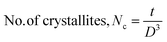
Using Scherrer's formula, the crystallite size was determined as
| |
 | (1) |
Here,
β is the full width at half maximum.
k (Scherrer's constant) = 0.9. The other different quantities were evaluated as follows
27,28| |
 | (2) |
| |
 | (3) |
| |
 | (4) |
Here, ‘
t’ stands for film thickness. The FWHM values of the In
10Se
70Te
15Bi
5 thin films were obtained through Gaussian fitting of the XRD peaks using the origin software. The corresponding standard deviation (
σ) values were derived from the fitting parameters, following the relation FWHM = 2.355
σ. The step size of 0.02° per step provides adequate angular resolution.
The crystallinity first increases from 18.95 nm to 20.04 nm and then decreases to 14.76 nm upon 60 min laser irradiation, whereas values of other parameters like ε, δ, and N increase with an increase in irradiation time. While the addition of bismuth in In10Se70Te15Bi5 thin films can enhance crystallinity during laser annealing, the observed decrease in crystallinity with prolonged annealing is likely due to thermal effects, partial melting, and defect formation, which outweigh bismuth's positive influence. Similar observations have been reported in other thin film systems, such as BiTeCl and BiFeO3, where extended annealing led to crystallinity degradation and phase transformations. However, upon laser irradiation, a slight reduction in peak intensity along with broadening of the diffraction peaks is observed. This behaviour indicates a decrease in crystallinity, which can be attributed to laser-induced disorder, structural defects, or partial amorphisation. The decrease in crystallinity may result from rapid thermal gradients during laser treatment, which can cause partial melting within the film. The localized thermal effects associated with laser irradiation can disrupt long-range order, reduce crystallite size, and generate internal strain, all of which contribute to the degradation of the crystalline phase. Khan et al. have found that similar reductions in crystallinity due to laser processing have been reported in related chalcogenide systems. In the future works HRTEM, AFM, and mass-loss analysis will be undertaken to directly visualize lattice defects and validate the mass-transport processes suggested by the current results.
3.2. FESEM and EDS surface morphology and composition
The film thickness was again cross-checked by a cross-sectional FESEM image (Fig. 3(b)) for the deposited film. It comes around nearly the same as that of the thickness found from the thickness monitor. It is observed that after illumination, the thickness remained nearly the same (Fig. 3(c)). The changes in the surface morphology were investigated using FESEM to examine the surface morphology of the sample by laser treatment. This technique provides insights into changes in grain structure, surface roughness, and uniformity due to laser-induced thermal and structural effects. The FESEM micrographs of In10Se70Te15Bi5 thin films before and after laser irradiation for 5, 10, 30, and 60 minutes (Fig. 4(a–e)) reveal significant morphological transformations. FESEM pictures are taken for 1 µm, is shown in Fig. S1.
 |
| | Fig. 4 FESEM micrographs of (a) 0, (b) 5, (c) 10, (d) 30, and (e) 60 min laser-treated In10Se70 Te15Bi5 thin films at 100 nm magnification scale. | |
The pristine film shows a smooth, dense surface with uniformly distributed nanograins. After laser irradiation, the surface exhibits larger grain size and the emergence of micro- or nano-scale texturing, indicating recrystallisation and surface modification. The presence of bismuth plays a key role in this morphological evolution. Due to its low melting point (∼271 °C) and tendency to segregate at grain boundaries, along with the thermal effect of the laser promotes atomic mobility, leading to particle agglomeration and improved crystallinity. Similar observations were reported for laser-irradiated morphology changes in other films.29
The distribution of various elements in the 60-minute irradiated film is evident from the mapping image (Fig. S2(a–e), SI file). The respective elements are distributed uniformly inside the film as seen from the pictures. The confirmatory data is shown with the peaks of respective elements in Fig. S2(f). The shell energy associated with the elements is reflected as the intense peak. The peak at 1.33 keV stands for Se-atom. Likewise, peaks at 2.56, 3.35, and 3.89 keV stand for Bi, In, and Te atoms. The EDS spectra of other films are illustrated in Fig. S3.
For all laser-treated In10Se70Te15Bi5 film samples, the particle size distribution was evaluated and is depicted in Fig. 5(a–e) for irradiation times of 0, 5, 10, 30, and 60 minutes, respectively. The combined bar diagram representation of particle size of un-irradiated and laser annealed In10Se70 Te15Bi5 thin films is displayed in Fig. S4. The mean particle sizes were found to be 20.01 nm, 20.7 nm, 18.21 nm, 17.28 nm, and 16.1 nm, corresponding to increasing laser exposure durations. It ensured that the particle size decreased as the time of laser irradiation increased. This decrease in size might be due to the thermal and photo-induced effects of the laser, which encourage local reorganization and surface atom desorption. Finer nanostructures are produced as a result of particle fragmentation and re-nucleation brought on by these processes. With prolonged irradiation, the laser-induced enhancement of atomic mobility aids in the fragmentation of larger agglomerates, thereby refining particle size.30
 |
| | Fig. 5 Particle size distribution of the (a) 0, (b) 5, (c) 10, (d) 30, and (e) 60 min laser-irradiated In10Se70 Te15Bi5 thin films. | |
The close agreement between the crystallite sizes obtained from Scherrer analysis and the particle sizes observed in FESEM indicates that the size reduction with increasing irradiation time is likely due to surface atom desorption and the de-aggregation of weakly bound crystallite clusters. This interpretation is backed by the progressive increase in dislocation density and lattice strain (Table 1), which suggests that laser exposure introduces structural disorder and defect formation within the lattice. These microstructural changes reflect a combined effect of localized heating, bond rearrangement, and enhanced atomic mobility under laser irradiation.
Table 1 Structural parameters of In10Se70Te15Bi5 thin films
| Structure parameters |
D (nm) |
δ × (10−4 nm−2) |
ε × 10−3 |
NC × 10−2 (nm−2) |
| As-prepared |
18.958 |
27.822 |
10.513 |
11.740 |
| 5 min |
20.043 |
24.891 |
10.864 |
9.936 |
| 10 min |
19.575 |
26.101 |
10.162 |
10.664 |
| 30 min |
18.603 |
28.890 |
09.130 |
12.425 |
| 60 min |
14.761 |
45.901 |
14.006 |
24.874 |
3.3. XPS study
XPS is a crucial method for examining surface chemistry of a material. It provides thorough information on chemical states, electronic structure, and elemental composition, all of which are essential for characterising and improving the properties of materials in a variety of applications.31 The XPS has been performed for the as-prepared and 60 min laser-irradiated In10Se70Te15Bi5 thin film sample. Fig. 6(a) shows the survey spectra, and Fig. 6(b–e) shows individual XPS core levels of In 3d, Se 3d, Te 3d, and Bi 4f, respectively.
 |
| | Fig. 6 Comparative XPS spectra of (a) full survey, (b) In 3d, (c) Se 3d, (d) Te 3d, (e) Bi 4f of as-prepared and 60 min laser-treated film. | |
The survey spectra (Fig. 6(a)) confirm the presence of In, Se, Te and Bi in both the as-prepared and 60 min irradiated films without any additional impurity-related features. A noticeable increase in overall peak intensity for the irradiated sample indicates enhanced surface cleanliness and improved elemental exposure after laser treatment. The core-level spectra of In 3d (Fig. 6(b)) show shifts from 444.4 eV and 452.0 eV in the as-prepared film to 444.97 eV and 452.61 eV for In 3d5/2 and In 3d3/2 orbit with a difference of 7.64 and 7.6 eV, respectively, after irradiation.32 A similar positive shift is observed for Se 3d, which moves from 53.82 eV to 54.92 eV (Fig. 6(c)). This binding energies (BE) confirms the presence of bonded selenium within the film matrix. It aligns well with previously observed values for selenium in metal selenide compounds.33 The Te 3d peaks also exhibit slight upward shifts (Fig. 6(d)), with Te 3d5/2 moving from 576.11 eV to 576.47 eV and Te 3d3/2 from 586.51 eV to 586.81 eV. This shows the BE gap of 10.4 and 10.34 eV, for as-prepared and 60 min irradiated sample. This arises from the spin–orbit splitting and is characteristic of Te in its chemical environment.34 The Bi 4f peaks (Fig. 6(e)) distinguished at 160.91 eV and 166.65 eV for laser irradiated and 160.99 eV and 166.26 eV for as-prepared films are assigned to Bi 4f7/2 and Bi 4f5/2 spin orbits. This shows the spin–orbit splitting of 5.27 and 5.54 eV in both the cases, which is a modest but consistent shifts to higher BE as well. This splitting arises due to the interaction between the spin and orbital angular momentum of the electron, and the observed BE are consistent with the existence of bismuth in the +3 oxidation state (Bi3+). These findings support the bonding environment and chemical state of Bi in the thin film matrix, which is crucial in estimating the optical and electrical characteristics of the material.35 These systematic increases in BE suggest that laser irradiation promotes mild surface oxidation and alters the local chemical environment of the constituent elements. Such changes are attributed to localized heating, enhanced atomic mobility and the redistribution of surface defects during irradiation. The XPS findings therefore support the structural and morphological evolution observed in XRD and FESEM analyses, confirming that laser treatment influences both the surface chemistry and bonding characteristics of the films.
3.4. Optical quantities (linear parameters)
3.4.1. Transmittance, absorption coefficient, and optical bandgap. The optical significance is viewed through the transmission power of the sample. The optical transmission data of various laser-treated In10Se70Te15Bi20 films over 600–2500 nm wavelengths are presented in Fig. 7(a). It shows the reduction of transmission with increasing laser time. The observed small fringe pattern arises due to interference between reflections from the substrate and the film layer, indicating uniformity in the film thickness.36 Weak absorption over 900–1200 nm wavelength is assigned to localised states created by disorder and defects in semiconductors. Upon laser irradiation, the optical transmission of the In10Se70Te15Bi5 thin film decreases from 75% to approximately 60% for 60 min of laser irradiation at around 2000 nm. However, in the longer wavelength region near 2500 nm, the transmission increases again to about 70% after 60 minutes of laser exposure. The competing effects of laser-induced disorder and thermal restructuring can explain this non-monotonic trend in transmission behaviour. The initial decrease in transmission may be attributed to laser-induced modifications such as the formation of localised defect states, increased surface roughness, or enhanced structural disorder, which promote additional light scattering and absorption.37 These effects are common in chalcogenide systems where photon energy induces bond rearrangements and defects. The recovery of transmission at higher wavelengths after prolonged laser exposure could be associated with localised annealing effects, which improve the film's homogeneity and reduce optical losses. Such behaviour has been reported in laser-irradiated chalcogenide films, where grain growth and structural reordering contribute to improved infrared transparency.38 It insights absorption edge shifting toward lower energy, and the optical constants are affected, contributing to the observed reduction in the bandgap by defining the photodarkening nature of the film.
 |
| | Fig. 7 Variation of (a) T%, (b) ‘α’ with the wavelength of In10Se70 Te15Bi5 thin films. | |
The absorption coefficient (α), signifying the rate of absorption of light by the studied films, was determined through39
| |
 | (5) |
With ‘
t’ as the film thickness. The variation in ‘
α’ of the In
10Se
70Te
15Bi
20 films is illustrated in
Fig. 7(b). The “
α” values reduced with wavelength and more for 60 min laser-treated film. It signifies more transparent behaviour at low energies. With increasing laser irradiation duration, the values of ‘
α’ showed an upward trend. The PD effect is evident from the shift of the absorption edge towards longer wavelengths. This shift leads to a redshift in optical absorption and a corresponding decrease in transmittance, as also observed in the present films. The increase in ‘
α’ values during irradiation indicates an enhancement in localised states, leading to a decrement in
Eg and alterations in the film surface.
40
For evaluating the bandgap at high absorption area (α > 104 cm−1), the Tauc relation is used. As per Tauc relation41
Here,
B represents the Tauc parameter. It gives the degree of structural randomness inside the sample. The exponents,
p = ½, 2 are for direct allowed and indirect allowed transitions. Likewise,
p = 3/2, 3 for direct prohibited and indirect prohibited transitions. In the present case,
p = 1/2 fits well to the data, thus inferring the direct allowed type bandgap.
Fig. 8(a–e) illustrates the fitting of (
αhυ)
2 against (
hυ). The
x-intercept represents the
Eg value, while slope yields Tauc parameter. The obtained
Eg and ‘
B2’ values are given in
Table 2. As the exposure duration increases, a reduction in “
Eg” is observed, indicating PD behaviour. Such a decrement is by the formation of new energy levels near the valence band with prolonged irradiation, resulting in the creation of pathways, referred to as localised states, that facilitate electron transitions from one band to another band. These localised states possess energies lower than the original bandgap of the material.
42
 |
| | Fig. 8 (a–e) Bandgap variation estimated with Tauc relation for In10Se70Te15Bi5 films. | |
Table 2 Optical parameters of In10Se70Te15Bi5 thin films
| Optical parameters/time in minutes |
0 |
5 |
10 |
30 |
60 |
| Direct bandgap (Eg) eV |
1.368 |
1.353 |
1.348 |
1.341 |
1.330 |
| Tauc parameter (B2) (×1010) cm−2 eV2 |
6.42 |
5.67 |
5.23 |
5.10 |
4.85 |
| Static linear refractive index (n) |
3.077 |
3.087 |
3.091 |
3.096 |
3.103 |
| χ(1) |
1.963 |
1.978 |
1.983 |
1.990 |
2.001 |
| χ(3) (×10−8 esu) |
1.524 |
1.543 |
1.552 |
1.562 |
1.577 |
| n2 (×10−7 esu) |
1.866 |
1.885 |
1.892 |
1.901 |
1.915 |
| Optical electronegativity (ηopt) |
2.880 |
2.876 |
2.874 |
2.872 |
2.868 |
| High-frequency dielectric constant (εL) |
9.47 |
9.53 |
9.55 |
9.58 |
9.63 |
The mechanism behind this Eg reduction lies in the absorption of laser photons by the thin film. This absorbed energy is primarily converted into vibrational energy, which is sufficient to break weak or metastable bonds, especially in chalcogen-rich amorphous systems. As these bonds are broken, the system gains translational degrees of freedom and increased thermal energy, effectively raising the local heat capacity.43 These changes enhance atomic mobility and promote structural rearrangement, contributing to crystallisation and narrowing of the band gap. In materials like In–Se–Te–Bi, which possess a complex bonding network, the introduction of Te and Bi can influence bond stability and optical response. Te tends to lower the band gap due to its higher atomic mass and polarizability. At the same time, Bi can act as a defect-inducing agent, enhancing localised states within the band structure.44,45
Laser-induced bond disruption in such a system leads to increased disorder, formation of localised energy states within the gap, and hence a further reduction in Eg.46 The enhancement in density of localised states leads to a narrowing of Eg and enhances the likelihood of electronic transitions from the band-tail states. This trend is consistent with earlier reports in the literature.47 Tauc parameter (B2), which reflects the extent of band tailing, is inversely related to the degree of structural order. In this study, a systematic decrease in B2 values with increased exposure time (Table 2), suggests a progressive increase in structural disorder within the thin film.
3.4.2. Skin depth (δ), optical density (OD) and extinction coefficient (k). The skin depth is the characteristic penetration length of electromagnetic waves through the sample. The intensity of primary radiation attenuates in an exponential way with depth. It is defined as the reciprocal of absorption coefficient, δ = 1/α. As illustrated in Fig. 9(a), δ decreases with hν, reflecting stronger absorption at higher energies. The δ value reduced with illumination time (Fig. 9(a)). Physically, this reduction in skin depth with increasing hν suggests stronger electronic transitions due to higher photon energies, which limit the wave's ability to penetrate deeper into the film. The shift in cut-off energy with prolonged laser exposure can be attributed to structural reordering, crystallisation, or defect state formation. Laser irradiation modifies the thin film's microstructure, thereby influencing its absorption edge and optical constants. This behaviour aligns with previous findings in similar chalcogenide systems,12,48 where increased laser fluence or exposure time resulted in decreased band gap, enhanced absorption near the edge, and reduced ‘δ’. Such a trend supports the observed shift in optical constants induced by laser irradiation. In the present study, laser irradiation resulted in a reduction in Eg, which is accompanied by a corresponding decrease in skin depth (δ); this reduction enhances optical confinement, suggesting the suitability of these films for use in multimode optical fibre applications with tuneable modal properties.49
 |
| | Fig. 9 Variation of (a) skin depth, (b) OD, (c) ‘k’ variation of In10Se70 Te15Bi5 thin films. | |
Optical Density (OD) is a critical parameter that reflects the absorption strength of a material. It provides insights into both the material's concentration and surface morphological changes, particularly under external stimuli such as laser irradiation. The OD is mathematically determined using the relation:50 OD = α × d with d as the film thickness. Fig. 9(b) depicts the increased OD value with time of irradiation. Therefore, the increase in OD complements the reduction in Eg observed in the irradiated films, confirming that laser treatment not only affects optical absorption but also influences the underlying electronic structure of the material.51
The interaction between light and matter, particularly the material's capacity to absorb light, is quantitatively described by the extinction coefficient (k). This optical parameter is a measure of the material's absorbing power and is directly related to how much light is attenuated as it propagates through the medium. The extinction coefficient is determined using the relation.52  . Fig. 9(c) infers the change of ‘k’ with photon wavelength for all investigated films. The increased pattern of ‘k’ with exposure time indicates the annealing out of unsaturated bonds with creation of saturated bonds. It helps for the increased k value.53
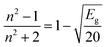
3.4.3. Linear static refractive index (n), high-frequency dielectric constant (εL), optical conductivity (ηopt). The refractive index (n) characterises the dispersion of light waves and other nonlinear optical phenomena in a material. The value of n can be estimated from the optical bandgap (E9) using the Dimitrov and Sakka empirical relation. This relation provides a useful link between the electronic band structure and the optical dispersion behaviour of the material54| |
 | (7) |
With increasing laser exposure time, the refractive index (n) exhibited a notable enhancement (Table 2). Materials possessing elevated n values are of considerable interest due to their potential to improve optical confinement and light–matter interaction. In the present case, n values were found to vary between 3.07 and 3.10, suggesting their suitability for applications in integrated photonic devices, ultrafast optical modulators, infrared (IR) sensors, and related optoelectronic systems.55 The reverse trend of “Eg” with “n” value follows Moss's rule, i.e., Egn4 ∼constant.56 The Egn4 ∼constant leads to as,
with ‘k’ = 95 eV. The modified For calculation of ‘n’ below 4 eV materials, Ravindra's relation nR = 4.084 [0.62 × Eg] is used.57 In a similar note, for less Eg value materials, Herve–Vandamme58 relation is used. It is based on oscillator theory, expressed as,
where, A ≅ 13.6 eV, (∼hydrogen ionisation energy), and B = 3.4 eV. The difference in energy between Eg and UV resonance energy is denoted as ‘B’. Considering these values, the above relation becomes
The exponential decay of ‘n’ for semiconductors with band gaps is given by Tripathy,59 the relation, nT = 1.73 × [1 + 1.9017 × e−0.539×Eg]. The relation is valid for a wide frequency regime. The values obtained from different models are expressed in Fig. 10(a). It presents the inverse variation with Eg values.
 |
| | Fig. 10 (a) Refractive index change, (b) change in Eg and χ(3), (c)Change in Eg and n2 with irradiation time of the In10Se70Te15Bi5 thin films. | |
The high frequency dielectric constant is obtained from εL = n2. It is attributed to the electrical polarizability of the material. In the current case, it is increased with irradiation time (Table 2). The εL is associated with free charge carriers that influence polarisation in the material. The optical conductivity (ηopt) is evaluated from,  , with c = 25.54 and are given in Table 2.60 Basically, it is the affinity of an atom for the formation of a bond. Here, it decreased from 2.880 (un-irradiated) to 2.868 for a 60-minute laser-treated film (Table 2). The very less change indicates the film stability with laser irradiation.
3.5. Non-linear optical behaviour
The nonlinear optical phenomenon primarily focuses on enabling ultrafast optical switching devices and plays a crucial role in modern communication sectors. This behaviour becomes significant when the material's polarisation response exhibits a nonlinear relationship with the incident electromagnetic radiation. The polarizability is intrinsically linked to the dielectric properties, that are obtained from ‘n’ and ‘k’. The refractive index is particularly associated with the material's nonlinear optical characteristics. Consequently, any external energy input that alters the host matrix can lead to a subsequent change in susceptibility. So, materials exhibiting high optical nonlinearity hold significant promise for different applications.61,62 The induced polarisation (P) varies nonlinearly with the applied electromagnetic field (E), but instead follows a power-series expansion. The polarisation density (P) can be expanded as63| | |
P = εoχE = εo[χ(1)E + χ(2)E2 + χ(3)E3…
| (8) |
Here, εo stands as the electrical permittivity of free space. χ is net susceptibility. It contains linear and non-linear components, χ = χ(L) + χ(NL) with χ(L) = χ(1) and χ(NL) = χ(2) + χ(3). Here χ1, χ2, and χ3 are 1st, 2nd, and 3rd-non-linear susceptibilities.
The nonlinear quantities χ(1), n2, and χ(3) are connected to the dielectric polarisation because of the application of an electric field on the films. For centrosymmetric media χ2 = 0, due to the absence of inversion symmetry. The χ(1) and χ(3) are obtained by the relation.64
| |
 | (9) |
Here,
A = 1.7 × 10
−10 esu. The estimated
χ(1) and
χ(3) values show a noticeable improvement with increasing laser exposure duration. This enhancement is likely attributed to laser-induced homogenization and polymerization inside the film structure. In turn, it elevates the carrier concentration.
65 Polymerisation enhances ‘
χ(3)’ by creating new and ordered systems suitable for non-linear interactions. Such structural transformations are essential for advancing non-linear optical applications, including sophisticated photonic devices.
66 Fig. 10(b) illustrates the ‘
χ(3)’ and
Eg, change with time, that shows the opposite trend.
3.5.1. Nonlinear refractive index (n2). Refractive index change (Δn) originated from the non-linear optical response. It is represented as, Δn = n2∣E∣2 with n2 as the nonlinear refractive index. The n2 of the studied films was determined through Ticha and Tichy and Miller's rule,64,67| |
 | (10) |
The value of n2 for different laser-treated films is given in Table 2. Fig. 10(c) presents the “n2” pattern with Eg for different exposure times. The enhancement of χ(3) and n2 by laser exposure can be ascribed to local structural alteration by changes in defect states, which consequently alter the material's local polarizability.66
3.6. Wettability analysis
The surface behaviour solely depends on its adhesion quality, which is evaluated through wetting properties. This is typically assessed by studying the interaction among a solid and a liquid in contact. The angle formed at the interface is known as the contact angle (θc). It serves as a quantitative indicator of the material's wettability. A low θc corresponds to more wettability (hydrophilic surface). Likewise, a high θc signifies less wettability (hydrophobic surface). Contact angle analysis thus provides crucial insights into the material's affinity for liquids. In this study, the as-prepared sample exhibited a contact angle of θc = 89°, and the 60-minute irradiated sample showed θc = 50° (Fig. 11). The measured angle shows the hydrophilic nature, and the decreased angle indicates the increased hydrophilicity with increased time scale. The variation in surface wettability is primarily due to the differences in surface roughness, as the identical composition across all samples minimizes the influence of surface tension. Thus, roughness becomes the key factor influencing wettability. As per the Cassie–Baxter model, trapping of air between the liquid and solid interfaces is less for smooth surfaces, allowing better water spreading. This explains why laser-irradiated films, which are more hydrophilic, enable water droplets to spread more efficiently, thereby reducing the buildup of dirt, dust, and fouling on the film surface. However, the decrease in water contact angle after laser irradiation is not solely due to surface roughness changes but also to surface chemistry modifications. As confirmed by XPS study in Section 3.3, the appearance of oxygen-related species and slight BE shifts indicate the formation of hydrophilic surface groups, which increase surface energy and enhance wettability. Such laser-induced surface oxidation leads to an increase in surface polarity and surface energy, which enhances hydrophilicity and contributes to the observed reduction in the water contact angle. Thus, both morphological and chemical changes contribute to the improved hydrophilicity of the laser-treated films. On the other hand, a low θc indicates a more solid–liquid interfacial area, which is influenced by surface morphology and free energy. As a result, the films exhibit potential for use in diverse applications, including self-cleaning, antifouling, and antifogging coatings.68,69
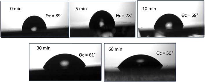 |
| | Fig. 11 θc picture of un-irradiated and irradiated In10Se70 Te15Bi5 thin films. | |
Young's formula determined the surface free energy by the relation,64
| |
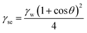 | (11) |
With
γw = 71.99 mN m
−1 (water surface tension) and
γse as surface free energy. The
γse values are given in
Table 3, which shows the overall enhancement from 18.62 to 48.56 mN m
−1 with exposure time. In addition to surface energy, adhesion is another key factor influencing the wetting behaviour. Adhesion refers to the molecular desirability that occurs among in contact solid surfaces. The interaction strength among the water droplets and the thin film surfaces was evaluated through the work of adhesion (
Wsl). It was calculated from Young–Dupré equation,
70 | |
Wsl = γw(1 + cos![[thin space (1/6-em)]](https://www.rsc.org/images/entities/char_2009.gif) θ) θ)
| (12) |
The
Wsl for all the films was found to be increasing from 73.24 to 118.25 mN m
−1 upon irradiation (
Table 3).
Table 3 Contact angle data for as-prepared and irradiated In10Se70Te15Bi5 thin films
| Parameters |
θc (degree) |
γse (mN m−1) |
Wsl (mN m−1) |
| Laser-0 min |
89 |
18.62 |
73.24 |
| Laser-5 min |
78 |
26.25 |
86.95 |
| Laser-10 min |
68 |
34.14 |
99.16 |
| Laser-30 min |
61 |
39.67 |
106.89 |
| Laser-60 min |
50 |
48.56 |
118.25 |
3.7. Photoresponse study by I–V measurement
For photodetection studies, In10Se70Te15Bi5 thin films were prepared by scraping the edges to retain a 0.25 cm2 active area on a glass substrate. Ag paste was used at opposite sides of the film to form conductive contacts, which were connected to a Keithley 2450 Source Measure Unit (SMU) using two probes. A 9 W white LED bulb served as the illumination source during ambient condition testing, chosen for its broad visible spectrum and minimal thermal impact.
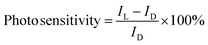
Fig. 12(a and b) shows the I–V behaviour (logarithmic) of the films under two conditions (light and dark), whereas the individual and combined linear plots of samples is detailed in Fig. S5 and S6 respectively. All samples display symmetric I–V curves and consistently higher photocurrent compared to dark current, indicating effective light-induced charge separation. Maximum current values (under illumination and in the dark) were extracted from Fig. S6 and tabulated in Table 4. Photosensitivity was computed using a standard formula, revealing notable sensitivity in some samples.71 Key photodetector metrics like-photoresponsivity (R) and detectivity (D*), were also calculated and included in Table 4 to evaluate device performance.
| |
 | (13) |
| |
 | (14) |
| |
 | (15) |
In this context,
A denotes the active area of the photodetector (0.25 cm
2),
Pin refers to the incident light power density (∼20 mW cm
−2),
e is the elementary charge,
λ is the wavelength of the incident light, and
c stands for speed of light.
 |
| | Fig. 12 Logarithmic representation of the I–V plots of all the In10Se70Te15Bi5 films in (a) dark and (b) light conditions. | |
Table 4 The figure of merit of all the as-prepared and laser-irradiated In10Se70Te15Bi5 thin films
| Sample |
IL (A) |
ID (A) |
IL − ID (A) |
Photo sensitivity (%) |
Responsivity (R) (A W−1) |
Detectivity (D*) (Jones) |
| 0 min |
1.73 × 10⁻⁷ |
1.59 × 10⁻⁷ |
1.34 × 10⁻⁸ |
8.39 |
3.46 × 10⁻⁵ |
7.66 × 10⁷ |
| 5 min |
3.74 × 10⁻⁷ |
2.84 × 10⁻⁷ |
9.09 × 10⁻⁸ |
32.02 |
7.49 × 10⁻⁵ |
1.24 × 10⁸ |
| 15 min |
2.71 × 10⁻⁶ |
2.5 × 10⁻⁷ |
2.07 × 10⁻⁷ |
8.29 |
5.42 × 10⁻⁴ |
3.02 × 10⁸ |
| 30 min |
7.55 × 10⁻⁶ |
7.2 × 10⁻⁷ |
3.53 × 10⁻⁷ |
4.9 |
1.51 × 10⁻³ |
4.97 × 10⁸ |
| 60 min |
1.26 × 10⁻⁵ |
1.17 × 10⁻⁷ |
9.04 × 10⁻⁷ |
7.72 |
2.52 × 10⁻³ |
6.51 × 10⁸ |
The I–V characteristics of laser-irradiated In10Se70Te15Bi5 thin films under both dark (Fig. 12(a)) and illuminated (Fig. 12(b) of the SI file) conditions demonstrate critical insights into their photoconductive behaviour. Films were subjected to varying durations of laser exposure (0, 5, 10, 30, and 60 minutes), and the electrical response was recorded across a ±10 V bias window. All curves exhibit symmetric I–V profiles, indicating ohmic contact behaviour between the silver electrodes and the thin film surface. This symmetry validates that the observed current changes originate from the material's intrinsic response to light and laser treatment, rather than contact-related artifacts. A consistent increase in current is observed under illumination compared to dark conditions for all laser exposure durations, confirming the photoconductive nature of the material.72 The photocurrent (IL) always surpasses the dark current (ID), which can be attributed to the generation of additional charge carriers upon light absorption and efficient carrier separation within the film.
Laser irradiation progressively modifies the electrical response: 0 min (as-prepared films) show the lowest current levels in both dark and light conditions. With increasing irradiation time (especially at 30 and 60 min), both dark and photocurrent increase significantly. This suggests that laser treatment induces structural or morphological changes (e.g., improved crystallinity, defect annealing, or compositional redistribution), which enhance charge carrier mobility and reduce recombination losses.73 The most pronounced enhancement is seen at 60 minutes, indicating a possible saturation point beyond which further improvements may plateau or degrade due to over-irradiation effects. The enhancement in photocurrent with laser exposure supports the hypothesis that laser treatment acts as a tuning mechanism for optimizing optoelectronic properties.74 Improved inter grain connectivity and reduced trap density could explain the higher current levels and better light response after extended irradiation. The I–V analysis reveals that laser irradiation significantly enhances the photodetection performance of In10Se70Te15Bi5 thin films. With increasing exposure time, both dark and light currents increase, demonstrating improved charge transport and light sensitivity.74 These findings position laser treatment as an effective post-deposition method for tailoring the electrical and optoelectronic properties of chalcogenide-based photodetectors.
Table 4 presents key photodetector figures of merit including photocurrent (IL), dark current (ID), photosensitivity, responsivity (R), and detectivity (D*) for In10Se70Te15Bi5 thin films subjected to different durations of laser irradiation (0–60 minutes). A general trend of increasing photocurrent (IL) is observed with laser irradiation, rising from 1.73 × 10⁻⁷ A (0 min) to 1.26 × 10⁻⁵ A (60 min). Simultaneously, the dark current (ID) fluctuates nonlinearly, initially increasing and then stabilizing or decreasing slightly. The maximum light-to-dark current difference (IL − ID) is recorded at 60 min (9.04 × 10⁻⁷ A), indicating improved photogenerated carrier transport at prolonged irradiation. Photosensitivity is calculated as the percentage increase in current under illumination, peaks sharply at 5 min irradiation (32.02%), significantly higher than both the unirradiated film (8.39%) and longer-irradiated samples (e.g., 4.9% at 30 min). This suggests that brief laser exposure may induce beneficial surface or defect states that enhance light absorption and charge separation. However, longer exposure could saturate or alter these states, leading to reduced sensitivity despite higher absolute current values. Responsivity (R) measures how effectively the device converts incident light into electrical current. It improves substantially from 3.46 × 10⁻⁵ A W−1 (0 min) to 2.52 × 10⁻³ A W−1 at 60 min, indicating enhanced quantum efficiency due to improved carrier mobility and reduced recombination. Similarly, detectivity (D*), which accounts for the signal-to-noise ratio, also increases consistently with irradiation time, reaching a peak of 6.51 × 10⁸ Jones at 60 minutes. This makes the 60-minute sample particularly suitable for low-light detection applications.
Interestingly, photosensitivity does not always correlate with R and D*. For instance, the 5-minute sample shows the highest photosensitivity but relatively low detectivity, likely due to its still-limited photocurrent. Conversely, the 60-minute sample, while showing slightly lower sensitivity, excels in both responsivity and detectivity due to enhanced charge transport properties. This points to a trade-off between fast surface-related enhancements and longer-term structural improvements induced by laser irradiation. The results indicate that laser irradiation is a powerful tool for tuning the optoelectronic properties of chalcogenide thin films. While short exposures enhance sensitivity likely via surface modification, longer treatments drive significant gains in responsivity and detectivity, likely by restructuring bulk film properties. The 60-minute irradiated sample offers the most balanced and high-performance photodetector behavior, making it a strong candidate for practical device applications.
4. Conclusion
This is the first systematic investigation of laser-irradiated In10Se70Te15Bi5 thin films focusing on the correlation between structural, optical, and photodetection properties. The influence of laser annealing on In10Se70Te15Bi5 thin films at different time scales is well evident from the electrical, structural, optical, and surface modifications. The photoresponsivity enhanced from 3.46 × 10⁻⁵ to 2.52 × 10⁻³ A W−1 and detectivity from 7.66 ×10⁷ to 6.51 × 108 by 60 min laser irradiation. Such enhanced values are good for photodetectors in the visible wavelength. This has resulted from the decrease in Eg value upon irradiation. The optical nonlinearity increased from 1.524 × 10⁻⁸ to 1.577 × 10⁻⁸ esu, and also the nonlinear refractive index from 1.866 × 10⁻⁷ to 1.915 × 10⁻⁷ esu upon laser irradiation for 60 min. The optical electronegativity was reduced; however, the dielectric constant increased from 9.47 to 9.63 upon laser treatment. The laser-induced surface changes were evident from the FESEM morphology and the surface wettability study. The decrease in contact angle indicates the increased hydrophilicity by laser illumination, which is helpful for antifouling and antifogging coatings. The static refractive index has been increased with the change in transmittance and absorption. The skin depth was reduced while the optical density was enhanced by laser treatment. The laser annealing also affected the structure by decreasing the crystallite size, thus increasing the dislocation density as evident from XRD. The observed modifications in the film properties by laser treatment is useful for various optoelectronic applications.
Author contributions
S. Giri: writing – original draft, data curation, investigation, methodology. Prabhukrupa C. Kumar: data curation, methodology, investigation. S. Supriya: data curation, methodology, investigation. D. Alagarasan: data curation, methodology, investigation. R. Naik: conceptualization, methodology, writing – review & editing, supervision.
Conflicts of interest
The authors declare that they have no known competing financial interests or personal relationships that could have appeared to influence the work reported in this paper.
Data availability
The data will be available from the corresponding author upon reasonable request. However, all the data used are presented in the manuscript and the supplementary information (SI) file. Supplementary information: details of FESEM, EDX, elemental mapping, particle size histogram, IV data. See DOI: https://doi.org/10.1039/d5ra06469d.
Acknowledgements
The author, Dr R. Naik, acknowledges the Science and Engineering Research Board, Govt. of India.
References
- A. H. Ammar, A. A. M. Farag and M. S. Abo-Ghazala, Influence of Sb addition on the structural and optical characteristics of thermally vacuum evaporated SbxSe1-x thin films, J. Alloys Compd., 2017, 694, 752–760 CrossRef CAS.
- A. M. Adam, E. Lilov, V. Lilova and P. Petkov, Characterisation and optical properties of bismuth chalcogenide films prepared by pulsed laser deposition technique, Mater. Sci. Semicond. Process., 2017, 57, 210–219 CrossRef CAS.
- I. Sharma, P. Sharma and A. S. Hassanien, Optical properties and optoelectrical parameters of the quaternary chalcogenide amorphous Ge15SnxS35-xTe50 films, J. Non-Cryst. Solids, 2022, 590, 121673 CrossRef CAS.
- R. Naik, R. Ganesan and K. S. Sangunni, Compositional dependence on the optical properties of amorphous As2-xS3-xSbx thin films, Thin Solid Films, 2010, 518, 5437–5441 CrossRef CAS.
- S. Das, S. Senapati, D. Alagarsan, R. Ganesan, S. Varadharajaperumal and R. Naik, Thermal annealing-induced transformation of structural, morphological, linear, and nonlinear optical parameters of quaternary As20Ag10Te10Se60 thin films for optical applications, ACS Appl. Opt. Mater., 2023, 1, 17 CrossRef CAS.
- Y. S. Obeng, N. V. Nguyen, P. K. Amoah, J. Ahn, M. Y. Shalaginov, J. Hu and K. A. Richardson, Dielectric spectroscopic investigation of reversible photo-induced changes in amorphous Ge2Sb2Se5 thin films, J. Appl. Phys., 2022, 131, 075102 CrossRef CAS.
- D. Sahoo, P. Priyadarshini, R. Dandela, D. Alagarasan, R. Ganesan, S. Varadharajaperumal and R. Naik, Investigation of amorphous-crystalline transformation induced optical and electronic properties change in annealed As50Se50 thin films, Opt. Quant. Electron., 2021, 53, 1–25 CrossRef.
- V. Kumari, A. Kaswan, D. Patidar, K. Sharma and N. S. Saxena, Electrical conduction mechanism in GeSeSb chalcogenide glasses, Bull. Mater. Sci., 2016, 39, 255–262 CrossRef CAS.
- A. S. Krymus, G. L. Myronchuk, O. V. Parasyuk, G. Lakshminarayana, A. O. Fedorchuk, A. El-Naggar, A. Albassam and I. V. Kityk, Photoconductivity and nonlinear optical features of novel AgxGaxGe1-xSe2 crystals, Mater. Res. Bull., 2017, 85, 74–79 CrossRef CAS.
- K. S. Bindra, N. Suri, P. Kumar and R. Thangaraj, Effect of Ag addition on the photoconductivity of amorphous Se–Sb thin films, Solid State Commun., 2007, 144, 83–87 CrossRef CAS.
- P. Abinash, D. Alagarasan, G. K. Pradhan and R. Naik, Time dependent 532 nm laser irradiation on quaternary Sb10S15 In15Se60 films: An insight into its structural, morphological, and optical modifications for photonics application, Phys. B, 2023, 657, 414785 CrossRef.
- P. Priyadarshini, A. Parida, D. Alagarasan, R. Ganesan and R. Naik, Time-dependent laser irradiation-induced kinetics of changes in linear–nonlinear optical properties of Bi15In20Se65 thin films for IR applications, J. Appl. Phys., 2023, 133, 063104 CrossRef CAS.
- S. Giri, P. Priyadarshini, D. Alagarasan, R. Ganesan and R. Naik, Annealing-induced phase transformation in In10Se70Te20 thin films and its structural, optical, and morphological changes for optoelectronic applications, RSC Adv., 2023, 13, 24955–2497 RSC.
- L. Liu, J. Dong, J. Huang, A. Nie, K. Zhai, J. Xiang, B. Wang, F. Wen, C. Mu, Z. Zhao, Y. Gong, Y. Tian and Z. Liu, Atomically resolving polymorphs and crystal structures of In2Se3, Chem. Mater., 2019, 31, 10143–10149 CrossRef CAS.
- M. Pandian, P. Matheswaran, B. Gokul, R. Sathyamoorthy and K. Asokan, Preparation and characterisation of indium chalcogenide thin films: a material
for phase change memory, Appl. Surf. Sci., 2018, 449, 55–67 CrossRef CAS.
- S. Pattipaka, P. Dobbidi, P. G. J, G. P. Bharti, G. Pradhan, S. S. K. Reddy, K. C. James Raju and A. Khare, Nonlinear optical properties of Bi0.5Na0.5TiO3 thin films grown by PLD, Ceram. Int., 2022, 48, 29533–29539 CrossRef CAS.
- S. Giri, P. Priyadarshini, D. Alagarasan, R. Ganesan and R. Naik, Influence of Te replacement by Bi in In10Se70Te20-xBix films and its structural, optical, morphological, surface wettability, and thermal behaviours for optoelectronic applications, Opt. Mater., 2023, 146, 114522 CrossRef CAS.
- P. Khan and K. V. Adarsh, Light-induced effects in amorphous chalcogenide glasses: Femtoseconds to seconds, Physics, 2021, 3, 255–274 CrossRef.
- S. S. Ashraf, Selenium-based amorphous semiconductors and their application in biomedicine, Electronic Devices, Circuits, and Systems for Biomedical Applications, 2021, vol. 2, pp. 25–46 Search PubMed.
- A. Aparimita, R. Naik, C. Sripan and R. Ganesan, Laser-induced optical photobleaching in Bi-doped Ge30Se70 amorphous thin films, Appl. Phys. A, 2020, 126, 5 CrossRef CAS.
- T. Halenkovic, M. Kotrla, J. Gutwirth, V. Nazabal and P. Nemec, Insight into the photoinduced phenomena in ternary Ge-Sb-Se sputtered thin films, Photonics Res., 2022, 10, 2261–2266 CrossRef CAS.
- M. Behera, N. C. Mishra and R. Naik, Laser irradiation-induced structural, microstructural and optical properties change in Bi-doped As40Se60 thin films, Ph. Transit., 2020, 93, 148–157 CrossRef CAS.
- D. Sahoo, P. Priyadarshini, R. Dandela, D. Alagarasan, R. Ganesan, S. Varadharajaperumal and R. Naik, In situ laser irradiation: the kinetics of the changes in the nonlinear/linear optical parameters of As50Se40Sb10 thin films for photonic applications, RSC Adv., 2021, 11, 16015–16025 RSC.
- M. Rashad, H. A. Saudi, H. M. H. Zakaly, S. A. M. Issa and A. M. Abd-Elnaiem, Control optical characterizations of Ta+5–doped B2O3–Si2O–CaO–BaO glasses by irradiation dose, Opt. Mater., 2021, 112, 110613 CrossRef CAS.
- M. Mohamed, S. Moustafa, A. M. Abd-Elnaiem and M. A. Abdel-Rahim, The optical parameters of γ-irradiated and annealed thin films of Ge15Se50Te35, J. Alloys Compd., 2015, 647, 771–777 CrossRef CAS.
- L. Pan, B. Song, N. Mao, C. Xiao, C. Lin, P. Zhang, X. Shen and S. Dai, Optical properties of Ge-Sb-Se thin films induced by femtosecond laser, Opt. Commun., 2021, 496, 127123 CrossRef CAS.
- P. Priyadarshini, S. Das, D. Alagarasan, R. Ganesan, S. Vardharajperumal and R. Naik, Observation of high nonlinearity in Bi-doped BixIn35-xSe65 thin films with annealing, Sci. Rep., 2021, 11, 21518 CrossRef CAS PubMed.
- A. Kumar, P. Heera and R. Sharma, Effect of compositional variation on the electrical properties of Se-Te-Bi-Ag glassy alloy, AIP Conf. Proc., 2015, 1661, 090007 CrossRef.
- M. I. Khan and A. Ali, Effect of laser irradiation on the structural, morphological and electrical properties of polycrystalline TiO2 thin films, Results Phys., 2017, 7, 3455–3458 CrossRef.
- P. R. de Moura, D. P. Almeida and J. C. de Lima, Photo-induced effects in chalcogenide thin films under irradiation by synchrotron light, J. Electron Spectrosc. Relat. Phenom., 2007, 155(1–3), 129–135 CrossRef CAS.
- S. Supriya, S. Das, S. K. Samal, S. Senapati and R. Naik, Rapid microwave-assisted synthesis and characterization of a novel CuCoTe nanocomposite material for optoelectronic and dielectric applications, Nanoscale, 2024, 16(15), 7566–7581 RSC.
- I. N. Reddy, Ch V. Reddy, M. Cho, J. Shim and D. Kim, Structural, optical and XPS study of thermal evaporated In2O3 thin films, Mater. Res. Express, 2017, 4(8), 086406 CrossRef.
- B. Robert, V. Flaud, R. Escalier, A. Mehdi and C. Vigreux, XPS study of Ge-Se-Te surfaces functionalized with organosilanes, Appl. Surf. Sci., 2023, 607, 154921 CrossRef CAS.
- S. Supriya, S. Das, A. Parida and R. Naik, Cu-doped CdTe nanoparticles synthesized by colloidal approach for optoelectronic and photodetector application, Mater. Res. Bull., 2025, 189, 113486 CrossRef CAS.
- S. Y. Jeong, K. S. Choi, H. M. Shin, T. L. Kim, J. Song, S. Yoon, H. W. Jang, M. H. Yoon, C. Jeon, J. Lee and S. Lee, Enhanced Photocatalytic Performance Depending on morphology of bismuth vanadate thin film synthesized by pulsed laser deposition, ACS Appl. Mater. Interfaces, 2017, 9(1), 505–512 CrossRef CAS PubMed.
- D. W. Kim, M. Kwon, S. Park, B. J. Kim and M. Cha, Measurement of the thickness and refractive index of a thin film by analysing reflected interference fringes, Appl. Opt., 2023, 62, 8018–8024 CrossRef PubMed.
- E. R. Shaaban, Optical constants and fitted transmittance spectra of varies thicknesses of polycrystalline ZnSe thin films in terms of spectroscopic ellipsometry, J. Alloys Compd., 2013, 563, 274–279 CrossRef CAS.
- P. Priyadarshini, D. Sahoo, D. Alagarasan, R. Ganesan, S. Vardharajperumal and R. Naik, Structural and optoelectronic properties change in Bi/In2Se3 heterostructure films by thermal annealing and laser irradiation, J. Appl. Phys., 2021, 129, 223101 CrossRef CAS.
- A. Aparimita, M. Behera, C. Sripan, R. Ganesan, S. Jena and R. Naik, Effect of Bi concentration on the structural and optical properties of BixGe30Se70−x chalcogenide thin films, J. Alloys Compd., 2018, 739, 997–1004 CrossRef CAS.
- N. Barreau, S. Marsillac, J. C. Bernède, T. BenNasrallah and S. Belgacem, Optical properties of wide band gap indium sulphide thin films obtained by physical vapour deposition, Phys. Status Solidi A, 2001, 184(1), 179–18 CrossRef CAS.
- J. Tauc, Amorphous and Liquid Semiconductors, Plenum Press, NewYork, NY, USA, 1979, p. 159 Search PubMed.
- Z. H. Khan, S. A. Khan, N. Salah, S. Habib, S. M. Abdallah El-Hamidy and A. A. Al-Ghamdi, Effect of composition on electrical and optical properties of thin films of amorphous GaxSe100−x nanorods, Nanoscale Res. Lett., 2010, 5, 1512–1517 CrossRef CAS PubMed.
- E. S. Zijlstra, T. Zier, B. Bauerhenne, S. Krylow, P. M. Geiger and M. E. Garcia, Femtosecond-laser-induced bond breaking and structural modifications in silicon, TiO2, and defective graphene: an ab initio molecular dynamics study, Appl. Phys. A, 2014, 114(1), 1–9 CrossRef CAS.
- A. El-Den and M. Fadel, Influence of tellurium content on the optical properties of In–Se–Te thin films, Appl. Surf. Sci., 2012, 258, 7507–7513 CrossRef.
- M. A. Wahab and A. Kumar, Effect of Bi addition on optical band gap of Se–Te chalcogenide glasses, Physica B, 2008, 403, 2434–2439 Search PubMed.
- M. Zhu, O. Cojocaru-Mirédin, A. M. Mio, J. Keutgen, M. Küpers, Y. Yu, J. Y. Cho, R. Dronskowski and M. Wuttig, Unique bond breaking in crystalline phase change materials and the quest for metavalent bonding, Adv. Mater., 2018, 30(18), 1706735 CrossRef PubMed.
- R. Naik, N. Behera and R. Ganesan, Laser-induced optical photo darkening in Sb30S40Se30 chalcogenide thin films, Adv. Sci. Lett., 2014, 20, 559–564 CrossRef CAS.
- S. Das, D. Alagarasan, R. Ganesan and R. Naik, Time-dependent 532 nm laser irradiation for tuning in optical, structural, and surface wettability changes of Te/In2Se3 optoelectronic applications, Surf. Interfaces, 2024, 53, 105029 CrossRef CAS.
- D. Biswas, R. Mondal, D. Mandal and S. Mondal, Investigation on Bi-induced changes on linear and non-linear optical parameters of As45Se(55-x)Bix chalcogenide glasses for photonic application, J. Non-Cryst. Solids, 2023, 614, 122401 CrossRef CAS.
- D. Alagarasan, S. Varadharajaperumal, D. A. Kumar, R. Naik, S. Umrao, M. Shkir, S. AlFaify and R. Ganesan, Influence of nanostructured SnS thin films for visible light photo detection, Opt. Mater., 2021, 121, 111489 CrossRef CAS.
- A. A. A. Darwisha, S. A. M. Issab and M. M. El-Nahass, Effect of gamma irradiation on structural, electrical and optical properties of nanostructure thin films of nickel phthalocyanine, Synth. Met., 2016, 215, 200–206 CrossRef.
- P. Priyadarshini, D. Alagarasan, R. Ganesan, S. Varadharajaperumal and R. Naik, Influence of proton ion irradiation on the linear–nonlinear optoelectronic properties of Sb40Se20S40 thin films at different fluences for photonic devices, ACS Appl. Opt. Mater., 2023, 1(1), 55–68 CrossRef CAS.
- M. A. Alvi, M. Zulfequar and A. A. Al-Ghamdi, Characterisation of phase change Ga15Se77Ag8 chalcogenide thin films by laser-irradiation, J. Alloys Compd., 2013, 550, 431–437 CrossRef CAS.
- V. Dimitrov and S. Sakka, Linear and nonlinear optical properties of simple oxides. II, J. Appl. Phys., 1996, 79, 1741 CrossRef CAS.
- I. Sharma, P. Sharma and A. S. Hassanien, Optical properties and optoelectrical parameters of the quaternary chalcogenide amorphous Ge15SnxS35−xTe50 films, J. Non-Cryst. Solids, 2022, 590, 121673 CrossRef CAS.
- T. S. Moss, A relationship between the refractive index and the infra-red threshold of sensitivity for photoconductors, Proc. Phys. Soc., 1950, 63, 167–176 CrossRef.
- H. Nyakotyo, T. S. Sathiaraj and E. Muchuweni, Effect of annealing on the optical properties of amorphous Se79Te10Sb4Bi7 thin films, Opt. Laser Technol., 2017, 92, 182–188 CrossRef CAS.
- P. Herve and L. K. J. Vandamme, General relation between refractive index and energy gap in semiconductors, Infrared Phys. Technol., 1994, 35, 609–615 CrossRef CAS.
- S. K. Tripathy, Refractive indices of semiconductors from energy gaps, Opt. Mater., 2015, 46, 240–246 CrossRef CAS.
- J. A. Duffy, Trends in energy gaps of binary compounds: an approach based upon electron transfer parameters from optical spectroscopy, J. Phys. C Solid State Phys., 1980, 13, 2979 CrossRef CAS.
- G. Nagpal, I. Sharma and S. Tripathi, The effect of the substitution of Sb with Zn on the optical and physical properties of Se90Sb10−xZnx (x=0,2,4,6,10 at.%) thin films, Nonlinear effects in optical fibres, origin, management and applications, Prog. Electromagn. Res., 2007, 73, 249–275 CrossRef.
- D. Sahoo, S. Sahoo, D. Alagarasan, R. Ganesan, S. Varadharajaperumal and R. Naik, Proton ion irradiation on As40Se50Sb10 thin films: fluence-dependent tuning of linear−nonlinear optical properties for photonic applications, ACS Appl. Electron. Mater., 2022, 4(2), 856–868 CrossRef CAS.
- H. Ticha and L. Tichy, Semiempirical relation between non-linear susceptibility (refractive index), linear refractive index and optical gap and its application to amorphous chalcogenides, J. Optoelectron. Adv. Mater., 2002, 4, 381–386 CAS.
- K. Anshu and A. Sharma, Study of Se-based quaternary Se-Pb-(Bi,Te) chalcogenide thin films for their linear and nonlinear optical properties, Optik, 2016, 127, 48–54 CrossRef CAS.
- A. A. A. Darwish and H. A. M. Ali, On annealing induced effect in optical properties of amorphous GeSeSn chalcogenide films for optoelectronic applications, J. Alloys Compd., 2017, 710, 431–435 CrossRef CAS.
- P. Priyadarshini, S. Das, D. Alagarasan, R. Ganesan, S. Vardharajperumal and R. Naik, Observation of high nonlinearity in Bi-doped BixIn35−xSe65 thin films with annealing, Sci. Rep., 2021, 11, 21518 CrossRef CAS PubMed.
- D. Kim, J. Park, J. Choi, J. W. Oh and Y. C. Kang, Compositional ratio effect on the physicochemical properties of SnSe thin
films, Physica B, 2021, 612, 412890 CrossRef CAS.
- C. Nefzi, B. Yahmadi, N. E. Guesmi, J. M. Garcia, N. Kamoun-Turki and S. A. Ahmed, A successful exploitation of gamma-radiation on chalcogenide Cu2InSnS4 towards clean water under photocatalysis approach, J. Mol. Struct., 2022, 1251, 131943 CrossRef CAS.
- A. B. Gurav, S. S. Latthe, R. S. Vhatkar, J. G. Lee, D. Y. Kim, J. J. Park and S. S. Yoon, Superhydrophobic surface decorated with vertical ZnO nanorods modified by stearic acid, Ceram. Int., 2014, 40, 7151–7160 CrossRef CAS.
- P. C. Kumar, S. Mohanty, J. Panda, S. Das, S. Supriya, D. Alagarasan and R. Naik, Enhanced photoresponse in a Ag2S/In2Se3 heterojunction-based visible light photodetector, RSC Adv., 2025, 15, 14518–14531 RSC.
- J. Zhu, L. Yu, Z. Wang, X. Wang, Y. Ou, M. Cai, Z. Wu, R. Tang, Y. Xia, Y. Wang and H. Deng, High-performance and stable Sb2S3 thin-film photodetectors for potential application in visible light communication, ACS Appl. Mater. Interfaces, 2023, 15, 28175–28183 CrossRef CAS PubMed.
- L. Mahapatra, S. Supriya, P. C. Kumar, D. Alagarasan, C. Sripan and R. Naik, Increase in photo sensitivity and detectivity of Bi/Sb35S35Se30 heterostructure films upon time-dependent laser irradiation for photodetection, Surf. Interfaces, 2025, 72, 107091 CrossRef CAS.
- A. Pandey, S. Sharma, A. K. Gangwar, M. Kaur, P. Singh and S. Husale, Strain-induced photocurrent enhancement in thin films of topological insulators (Bi2Te3), J. Mater. Chem. C, 2023, 11, 13838–13847 RSC.
- P. C. Kumar, S. Kanungo, P. Pradhan, S. K. Biswal, J. Kumar, C. Sripan and R. Naik, Tuning hydrophilicity and photoresponse by interfacial Ag diffusion in the Sb2S3 layer for optoelectronic applications: an experimental and computational study, J. Phys. Chem. C, 2024, 128, 16740–16753 CrossRef CAS.
|
| This journal is © The Royal Society of Chemistry 2025 |
Click here to see how this site uses Cookies. View our privacy policy here. 
 Open Access Article
 This Open Access Article is licensed under a Creative Commons Attribution-Non Commercial 3.0 Unported Licence
 a,
S. Supriyaa,
D. Alagarasanb and
R. Naik
a,
S. Supriyaa,
D. Alagarasanb and
R. Naik


 . Fig. 9(c) infers the change of ‘k’ with photon wavelength for all investigated films. The increased pattern of ‘k’ with exposure time indicates the annealing out of unsaturated bonds with creation of saturated bonds. It helps for the increased k value.53


 , with c = 25.54 and are given in Table 2.60 Basically, it is the affinity of an atom for the formation of a bond. Here, it decreased from 2.880 (un-irradiated) to 2.868 for a 60-minute laser-treated film (Table 2). The very less change indicates the film stability with laser irradiation.


