
 Open Access Article
 This Open Access Article is licensed under a Creative Commons Attribution-Non Commercial 3.0 Unported Licence
Organic electronics: pioneering the future of sustainable and flexible technology
Mohammed Bouachrine
 a and
Sahbi Ayachi
*b
a and
Sahbi Ayachi
*b
aMolecular Chemistry and Natural Substances Laboratory, Moulay Ismail University of Meknes, Morocco
bLaboratory of Physico-Chemistry of Materials (LR01ES19), Faculty of Sciences, University of Monastir, Avenue of the environment, 5019 Monastir, Tunisia. E-mail: ayachi_sahbi@yahoo.fr; m.bouachrine@umi.ac.ma
First published on 18th November 2025
Abstract
Organic electronics has evolved into a multidisciplinary field bridging molecular design, materials chemistry, and device engineering, enabling lightweight, flexible, and energy-efficient technologies that extend beyond the limits of traditional inorganic systems. This review provides a comprehensive and critical assessment of recent progress in sustainable organic and hybrid electronic materials, highlighting the interplay between molecular structure, processing strategy, and functional performance. The discussion spans conjugated polymers, small-molecule semiconductors, and bio-polymeric systems designed for transient and eco-compatible devices. Quantitative comparisons of mechanical, electrical, and environmental metrics (tensile strength, modulus, conductivity, biodegradability) reveal clear correlations between chemical architecture and device reliability. Emerging nanocomposite frameworks and additive manufacturing routes, including 3D-printable inks and hybrid nanofillers, are highlighted as transformative platforms for scalable and circular fabrication. In parallel, the manuscript examines end-of-life management, recyclability pathways, and life-cycle assessment perspectives, framing sustainability as a measurable design criterion rather than a conceptual goal. Finally, advances in nonlinear optical (NLO) organic materials and their integration into photonic and optoelectronic architectures are discussed as frontiers extending the functional reach of organic systems. By unifying structure–property correlations with manufacturing innovation and ecological responsibility, this review delineates the roadmap toward next-generation, high-performance, and environmentally sustainable organic electronic technologies.
 Mohammed Bouachrine | Professor Mohammed Bouachrine is a professor and researcher at Moulay Ismail University, Meknès, Morocco. A graduate of the University of Montpellier II – École Supérieure de Chimie (France), he has developed a distinguished academic career in organic and materials chemistry. His research focuses on the design, synthesis, and theoretical modeling of functional organic molecules and materials with applications in organic electronics, photovoltaics, pharmaceuticals, and sustainable energy. Prof. Bouachrine has authored more than 300 indexed publications in high-impact international journals and supervised around twenty PhD doctoral theses. Professor Bouachrine has also presented numerous invited lectures at national and international conferences, contributing to the dissemination of scientific knowledge. He is actively involved in international collaborations that foster research excellence and scientific innovation within Morocco and across the Maghreb region. |
 Sahbi Ayachi | Sahbi Ayachi is a Full Professor of Physics at the Higher Institute of Biotechnology of Monastir, University of Monastir, Tunisia. He received his PhD in Physics (2006) and his HDR (2013) from the Faculty of Sciences of Monastir, where he developed a strong background in π-conjugated materials and organic electronics. His research focuses on the design, and modeling of organic and hybrid materials for optoelectronic and nonlinear optical applications, combining experimental and theoretical approaches based on DFT and TD-DFT methods. Prof. Ayachi has authored or coauthored over 90 scientific publications and several book chapters in leading international journals. He actively collaborates with research groups in Morocco, Japan, Spain, India, and Italy, and serves as a reviewer for numerous international journals. His current research interests include molecular engineering of donor–acceptor systems, charge-transfer dynamics, and the development of novel organic materials for photovoltaic and photonic devices, and nonlinear optical (NLO) applications. |
1. Introduction
Organic electronics represents a transformative paradigm in materials science and device engineering, built upon the use of carbon-based semiconductors whose optoelectronic properties can be molecularly tailored. Unlike conventional inorganic electronics dominated by silicon and metal oxides, organic systems offer structural versatility, low-temperature processability, and mechanical flexibility, enabling lightweight, conformable, and energy-efficient devices suitable for emerging applications such as wearable sensors, flexible displays, and biodegradable circuitry.1–3 The molecular design freedom inherent to organic compounds allows precise modulation of band structure, charge mobility, and emission characteristics through chemical substitution, conjugation length, and supramolecular organization.4,5 These features have positioned organic materials at the forefront of sustainable and human-centric electronics.The evolution of the field over the past four decades has been guided by breakthroughs in conjugated polymers and small-molecule semiconductors, which have unlocked charge-transport behavior previously unattainable in organic solids. From the pioneering discovery of doped polyacetylene and the advent of conducting polymers to the commercialization of organic light-emitting diodes (OLEDs) and organic photovoltaics (OPVs), the trajectory of organic electronics illustrates a continuous refinement of molecular architectures and device integration.6–8 Today, the research focus extends beyond optimizing intrinsic mobility or luminescence efficiency to understanding how molecular order, interfacial phenomena, and processing conditions govern macroscopic performance.
In parallel, the convergence of theoretical modeling, computational chemistry, and advanced characterization has accelerated the rational discovery of high-performance organic materials. Quantum-chemical and density-functional-theory (DFT) approaches now enable predictive correlations between electronic structure and charge-transport pathways.9–12 This integration of computation with experiment has established a feedback loop in which design hypotheses can be tested virtually, guiding targeted synthesis and reducing developmental cycles. Such synergy underpins the current shift from empirical exploration to data-driven materials innovation.
Contemporary organic electronics research increasingly addresses the imperative of sustainability. While organic semiconductors intrinsically offer lower-energy fabrication and reduced material demand, their long-term viability depends on improved chemical and thermal stability, recyclability, and eco-compatibility. The incorporation of biopolymers and naturally derived matrices, for example, cellulose, chitosan, and silk fibroin, introduces biodegradability and circular-life potential, establishing a bridge between performance optimization and environmental stewardship.13,14 At the same time, emerging nanocomposite formulations and additive manufacturing techniques enable scalable, solvent-efficient production of flexible electronic components with tunable mechanical and electrical profiles, moving the field toward industrial relevance and sustainable mass manufacturing.15
In this context, organic electronics has evolved from a niche scientific curiosity into a comprehensive platform technology that unites chemistry, physics, and materials engineering. The present review critically examines this evolution, from molecular design principles to device functionality, while highlighting quantitative performance metrics, emergent fabrication paradigms, and sustainability considerations. By unifying these dimensions, the work aims to delineate the scientific and technological roadmap toward next-generation, high-performance, and environmentally responsible organic electronic systems.
2. First developments
The first steps initial progress in organic electronics started in the 1970s with the discovery of certain organic semiconductor materials capable of transporting an electric charge. A breakthrough for this person was the 1977 isolation of the highly conductive polymer polyacetylene by Hideki Shirakawa, Alan MacDiarmid, and Hideki Sato. For that work, they won the 2000 Nobel Prize in Chemistry.16 Polyacetylene (Fig. 1) revealed that some polymers, commonly considered insulators, can indeed conduct when they're doped with chemicals.17,18 The discovery inspired investigation into alternative organic materials that would allow for more efficient electronic conduction. Interest in conductive polymers accelerated in the early 1980s with a growing focus on materials that showed promising conductivities at room temperature, notably the synthetic polyaniline and poly(3-hexylthiophene).19 This was enabled by the progress in polymerization methods, which are also bulkier and less expensive to produce. Finding and studying these materials has been key in helping create flexible and lightweight electronics for new technologies, and they also serve as a great substitute for traditional inorganic semiconductors. In 1987, Steven Van Slyke and Eugen W. Choi invented organic light-emitting diodes, or OLEDs, devices that employ organic materials discovered through research.20 These diodes, which harness the luminescent properties of organic materials, revolutionized the display market because they are energy-efficient and are capable of producing a wider range of colors and sizes. Major steps have been made in the parallel development of thin-film organic field-effect transistors (OFETs) that allow high-precision current control of electronic circuits of any size.21 This led to the development of flexible integrated circuits, which was a new era in electronic business in which a novel fusion of chemistry and electronics can give a lot of applications extending from sensors to bioelectronics, including lightning systems. Organic electronics are not only allowing for the development of these novel materials and devices, they are also paving the way for future generations of engineers and scientists to be active in this exciting area of research. Delve vigorously on this front. This new wave of development has led to promising no-future-in-g TOC energy storage systems, organic batteries, and polymer-based solar cells.22,23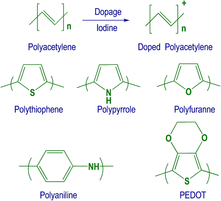 | ||
| Fig. 1 Conducting conjugated polymers and doping process of PA. | ||
Although the performances of these devices have slowly progressed over time, based on these primitive investigations into the electrical and optical characteristics of the organic components, they are still stuck in a suboptimal performance regime, at which the devices cannot deliver sufficient L and η, owing to the insufficient charge conduction and charge disposal properties. From flexible devices and information and communication technologies (ICT) to no-electronic, organic electronics has been an interdisciplinary field, connecting the chemists, physicists, and engineers. It is also burgeoning and updating.
3. Organic materials
Being carbon-based compounds, organic materials play a much more essential role than semiconductors in organic electronics, owing to their inherent properties. Their ductility, lightness, and versatility have contributed to considerable interest in the development of electronic, optical, and photovoltaic devices.24 We generally group organic materials into two major categories: conductive polymers and small organic molecules. Conducting polymers, like poly(3-hexylthiophene) (P3HT)25–28 and polyaniline,29–32 are easy to work with, quick materials that have a wide range of electrical and optical features and can be made cheaply using methods like printing or etching. Small organic molecules, such as fullerene and acene, have been used in the construction of organic photovoltaics because of their low cost of production as well as their increased functionality in some specific applications. The heterocyclic materials are inextricably tied to the scientific developments of the 1980s that enabled such semiconducting polymers.33,34 These advances formed the foundation for flexible electronics. This characteristic has been harnessed in the construction of devices including OLEDs, organic solar cells, and OFETs, systems that have revolutionized numerous fields from display technology to sustainable energy creation. At the same time, new projects utilizing additive techniques such as 3D printing have enabled the manufacture of sophisticated electronic circuits with unmatched precision.35 However, these materials face significant issues, primarily related to chemical stability and durability. Factors such as humidity and exposure to ultraviolet light do indeed affect the properties of organic materials, giving them a broader range in terms of extended applications. NWe will identify novel methods that focus on advanced formulation and structured forms of devices to enhance stability and durability while retaining their functionality. New discoveries in materials chemistry, and the latest way to create them, allows us to understand how electricity moves across organic material. Hence, these materials form a nexus of scientific hurdles and technological development, as the advance mentioned above is a big leap toward the future of electronics.3.1. Types of organic materials
Organic materials in general are divided into the following two categories: conductive polymers and organic semiconductors.Polyacetylene (Fig. 2) was identified in the 1970s, which was not only the exciting material taking a role in pure conducting organic materials.39 It has a chain of carbon atoms joined by alternating single and double bonds in such a way that adjacent pairs of carbon are also linked by a double bond, they are said to be part of the same or another conjugated system. Such a configuration provides an opportunity for electrons to travel through the chain, which is essential for conduction. But pure polyacetylene is, in fact, an insulator. It becomes conductive by adding other chemicals, like lithium chloride or iodine, which help create charge carriers (conduction electrons or holes). However, its low chemical stability confines the utilization of polyacetylene. In particular, upon contact with oxygen and moisture is readily decomposable, thereby rendering it less useful. However, polyacetylene opened the way for research on other stable and high-strength conductive polymers, and it still functions as an important standard material in studies on organic conductors.40 Its impact is still significant in the field of organic electronics, especially in making flexible and lightweight devices, although its stability limits it.
 | ||
| Fig. 2 Structure of polyacytelene (PA). | ||
Poly(3,4-ethylenedioxythiophene) (PEDOT) (Fig. 3) is probably the most frequently used and studied conducting polymer in the areas of electrochemistry and optoelectronics.41 As a member of the conjugated polymer family, the chemical structure of PEDOT is a carbon-based structure in which double and single bonds are alternating along the carbon chain of the main backbone; this structure in turn enables an electron density to exist along the chain, which makes it conductive. PEDOT is of particular interest thanks to its outstanding electric performance, chemical stability, and processability toward unlimited applications.42
 | ||
| Fig. 3 Synthesis of poly(3,4-ethylenedioxythiophene) (PEDOT). | ||
It was also well known that PEDOT was in many cases doped with other molecules, such as the sodium salt of polystyrene sulfonate (PSS), to increase its conductivity and perform its use in electronic applications.43 Through this blending, a flexible and stable conductor is formed, and the result can be used in a variety of applications, such as OLED displays, organic photovoltaic devices, and even supercapacitor electrodes. PEDOT can also be processed by straightforward fabrication methods, like deposition or imprinting, making it suitable for mass production using economic techniques. It has become much more stable, especially when compared to other conductive polymers like polyacetylene, even when exposed to oxygen and moisture, making it more appealing for long-term use. Cost-effective and remarkable electrical performance lead to PEDOT as a favorite material of flexible electronics as well as advanced technology in the energy and sensor sectors.44
Fullerenes (C60) (Fig. 4) are one of the well-known organic semiconductors.50 These tiny, soccer-ball-shaped carbon molecules are particularly effective at transforming light into electricity. In organic solar cells, fullerenes increase the efficiency of the charge-transport processes in the cell by absorbing the light and helping the electrons to move. Organic transistors also apply fullerenes to enhance the device performance of flexible electronics.51
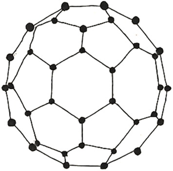 | ||
| Fig. 4 Schematic representation of fullerene (C60). | ||
Perylene diimide is also one of the important materials in this arena, due to its superior electronics properties, chemical robustness, and conductivity.52 These characteristics render it a material of choice for both advanced electrical applications and organic integrated circuits/energy storage devices (Fig. 5 & 6).
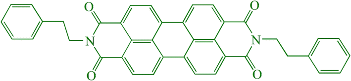 | ||
| Fig. 5 Perylene diimide. | ||
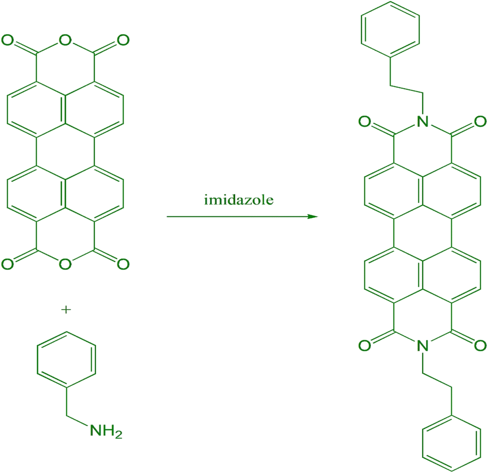 | ||
| Fig. 6 Synthesis of perylene diimide (PDEA). | ||
Perlyene diimide's (PDI) excellent chemical stability as well as long-term stability, where its performance has not degraded after many years, have made it an advantageous material for high reliability and more durable applications. These materials are enabling solutions that address today's challenging semiconductor designs, provide flexible pavement for continued innovation, and allow for the creation of new devices.53,54
4. Pioneering electronic devices
The introduction of the first electronic devices marked a significant milestone in the field of organic electronics, facilitating the transition from theory to practice. One of the earliest advances has been organic light-emitting diodes (OLEDs), which came in the 1980s (Fig. 7). They are used in displays, and have transformed the display industry because they generate light when an electric current is applied. These are usually prepared from organic materials placed as thin layers and the devices55,56 have the special characteristics that they are lighter (and in some case also more flexible) compared with the traditional technology (inorganic light emitting diodes (LEDs)). Organics are typically softer and lighter than the inorganic semiconductor silicon, so devices made with them can be thinner and more flexible. In addition, organic materials are being exploited in order to showcase their distinctive optical properties (e.g., highly effective light emitting ability) as well as create fresh prospects towards flexible displays, wearable devices and next-generation display technology.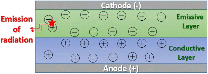 | ||
| Fig. 7 Schematic of a bilayer OLED. | ||
The polymer generally used in PLEDs is derivatives of poly(p-phenylene vinylene) or, more recently, certain polyfluorenes.57,58 These polymers are selected due to their good electroluminescent emission properties and their practical applications, particularly for large-area devices. Also, the choice of different side materials and the way the polymer is formed are very important for deciding the color of the light it emits, how it works, and how well it dissolves. In the course of developing such LEDs, an attempt was made to seek a substitute for the light emitting material. The color of the PEL emission can be vividly tuned by substituents, suggesting that such polymer could be an interesting emitter for the preparation of color tunable remote-controlled RGB OLED displays or lighting systems. Solubility is also a key factor in the fabrication of devices such as are the polymers that are amenable to processing by less costly printing or solution deposition. The non-substituted variants of PPV, for example PPV, are in general low soluble in their solvents. Soluble versions of PPV have been prepared for some similar soluble polymers and derivatives such as poly(vinyl naphthalene). These polymers can be prepared using ring-opening metathesis techniques and allow for easy precipitation, as they are polymerized in a stable cation and can be used in various milling and repulsion techniques. Although these materials are generally not used, various improvements can be considered in the field of hole injection, water-based derivative systems, and a blend of polymer.
5. Organic field-effect transistors
Another major development that repositioned organic electronics as an emerging field was the creation of organic field-effect transistors.59 The development marked the first case of using organic materials for the design of integrated circuits. Transistors increased energy efficiency in that they could be integrated into simple architectures and, thus, found enormous interest in a range of applications from sensors to storage devices. Besides enabling the prospect of more sustainable options, the finding has also fueled the development of lightweight, low-energy electronic devices based on organic materials. It is also worth mentioning that research is growing rapidly in the organic photovoltaic devices area. The systems show potential for achieving major improvements in access to renewable energy in off-grid and other localized communities, where established technologies are least deployed. These discoveries have opened new avenues for organic electronics and strengthened the momentum of research on the efficiency and sustainability of components. Thus, the trend has allowed for the extension of the limits of current devices, opening access to increasingly flexible electronic architectures.60 Overall, the groundbreaking discoveries in research have played a central role in the dynamics of redefinition, transforming electronic architectures into increasingly flexible and adaptable solutions. Thus, they pave the way for many other discoveries and possibilities for the future of electronics (Fig. 8).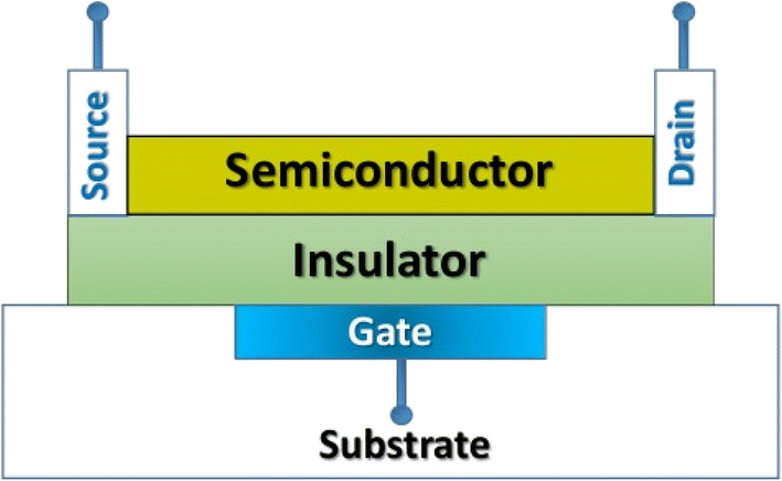 | ||
| Fig. 8 Schematic of an organic field effect transistor. | ||
Organic Field-Effect Transistors (OFETs) have been widely studied and reported in literature, using a large number of aromatic and conjugated materials as the active semiconductor layer. These include various polymers, which possess different electrical and mechanical properties to enhance OFETs' performance. Among these, polythiophenes, like poly(3-hexylthiophene) (P3HT), are some of the most researched because they have good qualities for moving charges and dissolving in solvents. Some other polymers used or proposed to be used for OFETs include polyfluorene, which has superior stability and optical characteristics, and polydiacetylene, having abnormal conduction properties.61,62 It should also be mentioned that p2T and p3T (both PPV-based as well as poly(2,5-thienylene vinylene)-based) are important as well in this context. They still feature an effective conjugation that is long enough and charge mobility that is high enough to make the OTFTs behave properly.
Those materials have also gone through extensive development, and in the past few years we have seen several excellent review articles summarizing at length the state of the art (focusing on the pros and cons of using it for organic electronics). These reviews provide important directions on the syntheses, properties, and device performance of these kinds of polymers, which drive research on these organic semiconductors.
6. Energy-related processes in organic electronics
The 1990s witnessed quite a lot of advancements associated with organic electronics, as it were, right energy research and developments. This period marked the emergence of organic materials for energy conversion and storage systems. The most interesting material proved to be conductive polymer, for example, poly(3-hexylthiophene) (P3HT), which is extensively utilized in efficient energy generation and storage. These materials are particularly appealing due to the inexpensive cost of their preparation, as well as their flexibility, and this renders them promising for several applications in devices such as photovoltaic cells and supercapacitors (for energy storage). The increasing efficiency of organic photovoltaic cells was one reason for this change. Cell efficiency has developed rapidly by optimizing the heterojunction structure and adopting the advances of cell production technology. New strategies such as introducing new nanomaterial and interface engineering have significantly improved the efficiency of converting light into electricity. These developments have created new opportunities, particularly in industries where the lightweight and flexible nature of the devices is essential, such as lightweight aviation, satellites, and portable electronic products.63 In the field of energy storage, organic batteries have gained particular interest due to the requirements for sustainable and environmentally friendly alternatives to classical heavy-metal-based batteries with environmental and sustainability concerns. Organic batteries are not only performing excellently, but they also hint at the ease of polluting the environment, therefore contributing to greener solutions.64 In addition to such studies, a vital research direction has been the use of organics for hybrid energy systems. Research is giving high strategic value to the combination of renewables (solar power technology) with organic-based storage energy devices. Serrano-Arévalo et al.65 integrate more hybrid system that would solve the problem of energy sustainability by minimizing the carbon print of energy generation and usage.7. The 2000s and the commercial industry
The 2000s introduced organic electronics to the world as a thriving commercial market. The decade saw a series of exciting new products for consumers, where the unique flexibility, light weight, and affordable production of organic materials played a big role in creating new electronic devices. Pioneering the way for a new technology standard, organic light-emitting diode (OLED) displays brought televisions, smartphones, and signage to market with image quality that was previously unimaginable. OLED displays have turned electronic devices not just good to look at but better for what you could do with them, for they can display richer blacks and more colors that are vibrant. Furthermore, technology created in that era had a fundamental impact on production techniques. Alternative manufacturing processes, such as printing organic circuits, were expected to cut down the production costs and to produce more complex and different designs. These new processes made new types of customizable product possible – form-factor defining “wearable” devices and flexible displays. In parallel, a large research and development effort produced new types of polymers and semiconductor materials that enabled organic electronic products to become more efficient and longer-lived.The increased collaboration between universities, companies and research institutions was key; it was instrumental to the invention and established crucial quality and performance benchmarks for the industrialization of such technologies. The ongoing exchange with these interlocutors further established organic electronics as an industry benchmark, and the technology finds itself as an essential part of the business strategy of leading companies within the tech sector. As such, the 2000s are not just a period of growth but a transformation in the development, manufacturing, and use of electronic technologies. The breakthroughs in new applications, innovations, and manufacturing technologies promoted organic electronics to take root at the centre of commercial affairs, setting a firm foundation for even deeper embedding in everyday life and strategic areas beyond this decade.
7.1. Consumer applications
Organic electronics have enabled new opportunities in consumer goods, with the incorporation of organic electronics in consumer products in the developed conglomerates. One key point of advancement is the invention of Organic Light Emitting Diode (OLED) displays, capable of providing even more saturated colors and increased contrast, coming into sight against other standard LED backlights.66 These types of displays, which are employed for modern televisions, smartphones, and computers, are flexible and lightweight and, thus, can be used for novel and aesthetically pleasing designs. For example, in recent years, OLED (organic light-emitting diode) TVs have gained increasing popularity due to the high quality of the display in response to the consumer's request for a more immersive visual.OLED lighting devices are increasingly being used in our homes. Due to the small form factor and moderate-to-high light efficiency, a variety of lighting scenarios, from accent lighting to effect lighting, can be realized with these luminaires. The integration of organic electronics in this regard fulfils not only aesthetic requirements but also is a step towards lower power consumption, which is increasingly emphasized in contemporary society. OLED lighting products are pervasive as a sustainable approach vis-à-vis conventional technologies, blending innovation and ecology.
Besides the displays and lighting, organic electronics have also been demonstrated in wearable components such as circuits and efficiency of power management, by which they can reduce the circuit's size and energy consumption. There are efforts to develop health-monitoring devices with organic sensors for noninvasive and real-time monitoring of human body data. Finally, the increasing integration of organic electronics into the consumer applications market is a testimony not only to the way that the technology can adapt to meet ever-changing consumer requirements but also to the potential it has to shape the way we interact with our technological surroundings.67,68
7.2. Technological innovations
The technological breakthroughs in organic electronics in the 2000s were tremendous, opening up avenues for many commercial applications. The main advancements that allowed for these applications are improving the performance of organic semiconductors to be closer to that of inorganic ones (Fig. 9) and creating tandems, thanks to significant improvements in the qualities of organic materials, which made them good alternatives to inorganic materials for better and more reliable devices.69–71 The outperformance of polyaniline and P3HT is probably due to the refinement of synthetic methodologies and a greater knowledge of their structure. That work laid the groundwork for OLED (organic light-emitting diode) displays, which, by replacing conventional LCD technologies,72 offer superior color depth, require less power, and can be bent.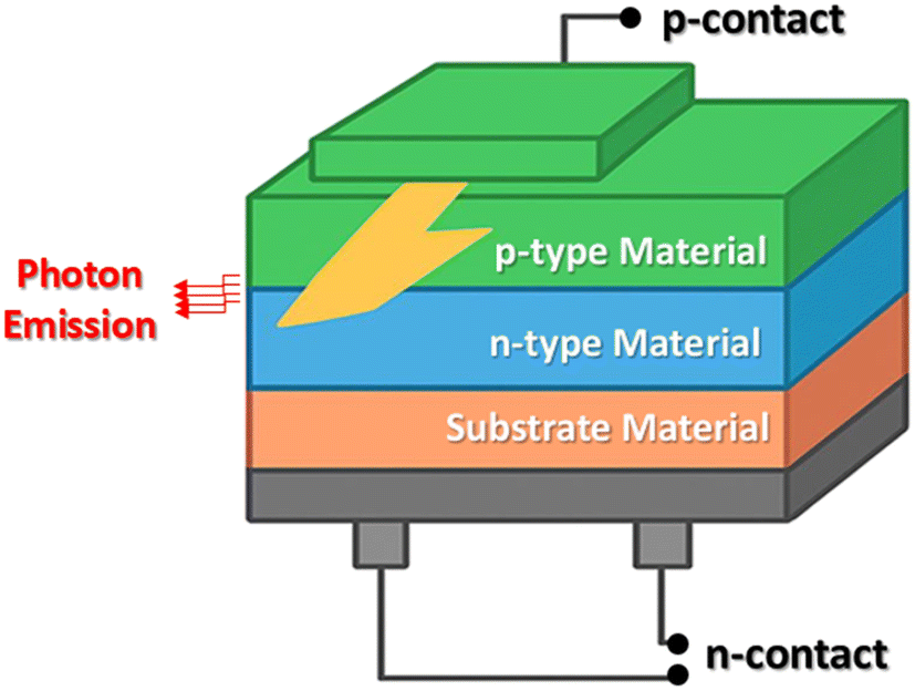 | ||
| Fig. 9 An inorganic LED (p-contact, p-type material, n-type material, substrate material, and n-contact). | ||
At the same time, new manufacturing methods like printing-based lithography and thin film deposition have made it cheaper to produce devices while also improving their size and clarity. These new production methods have, for example, allowed the making of organic printed circuits (the type of circuit you would want for a flexible surface you'd have in smart packaging or interactive clothing). Moreover, the development of the manipulation of structures at nanoscale gave birth to more compact, integrated devices, widening the horizon in which innovation can occur, such as in the fields of health or lighting, for example.
Finally, we wish to remark that interdisciplinarity was a key element in these breakthroughs, involving researchers in the areas of chemistry, physics, engineering, and materials science. Furthermore, cooperation among universities, research institutes, and private industries enables the flow of knowledge through the development of complementary skills and builds up the momentum for technological advancement. These developments are shaping not only the manufacturing industry but also the future of how technology is designed in general and turning organic electronics into the foundation of a sustainable, connected world.
8. Organic electronics in investigational studies
Organic electronics is a rapidly growing research area that leads to numerous technological applications because of its innovative materials and performance characteristics. At the core of this revolution, the central targets concern the design of new electronic devices, including organic field-effect transistors (OFETs), organic light-emitting diodes (OLEDs), and organic solar cells (OSCs). The devices have several attractive properties such as flexibility, and lightweight, low cost due to its printing process. The work in future aims at improving performance, longevity and scalability, overcoming the challenges that organic materials have to deal with (such as, performance and long-term stability). The collaboration with foreign companies is essential for the development of organic electronics. Multinational laboratories and commercial organizations are participating in multidisciplinary initiatives to disseminate knowledge and to accelerate technology development. For instance, European, Asian, and U.S. research groups have established consortia to investigate novel device architectures that include hybrid composites fabricated from organic and inorganic materials. These collaborations enhance not just the technical capabilities of current technology but also expand into new areas by exploring the potential use of organic electronics in new sectors, such as medicine, wherein the development of biological sensors or non-invasive diagnostics could change the face of many current standard practices. To sum up, directed research activities and international cooperation are enabling organic electronics to emerge as a major player in technological progress today. The integration of academic and industrial activities worldwide facilitates interactions among ideas, techniques, and material resources, pushing research toward attractive frontiers that may lead to a new paradigm for current electronics and broaden the practical uses of these materials.8.1. Key research projects
The development of organic electronics is based on some key research actions that have defined directions for its further growth as well as practical use. Among these projects, the PHOTONICS project funded by the European Union had greatly contributed to establishing the organic materials as materials for photonic devices. This ambitious initiative's aim was to develop revolutionary applications based on OLEDs and advanced photo-detection technologies that are both sustainable and energy-efficient. PHOTONICS convergence of researchers from multiple disciplines over the last few years, the convergence of researchers from differing scientific fields in PHOTONICS has pushed back the limits of what is technically feasible in achieving the best performing systems with the least environmental impact.73 This project was a turning point in that it demonstrated that existing equipment could not only be replaced by organic materials but also that the energy efficiency and flexibility could exceed that of the existing system.74 Another key project is the organic LED consortium, which has brought together major industry names like Philips, Panasonic, and other major players in electronics. This consortium has facilitated a dynamic exchange of knowledge between academia and industry while accelerating research on OLED production techniques. Due to the infusion of advanced technologies and the development of materials and manufacturing techniques, this project has made sustainable commercialization of high-performance OLED displays for televisions, smartphones and consumer electronics applications and has significantly affected the visual entertainment and consumer technology.75 At the same time, the OPV4ALL project, dedicated to organic solar panels (OPV-organic photovoltaics), opens new perspectives in the renewable energy sector. The work demonstrated the promise of low-cost and environment-friendly conductive polymers to replace noble metals in the fabrication of photovoltaic devices. Due to the organic PV cell technology and its professional material optimization variety of designs OPV4ALL project76 made significant steps ahead in performance as well as decrease of manufacturing costs and increasing of the energy harvest. These projects have contributed to the increasingly assertive role that organic electronics has taken in many fields, such as the display industry, renewable energies, and sensors. In this context, researchers and industry have become delicate, interdependent cooperation partners, sharing their resources to solve technology and environmental challenges. By enabling an intellectual exchange and fostering synergistic innovation, researchers and industry partners have expedited the development of flexible, business-oriented, and eco-friendly electronics. Organic electronics, through focused research efforts, are well poised to assume a significant role in the revitalization of tomorrow's technology and thus in providing crucial contributions to industry and society.778.2. The next generation of organic electronics
The prospects for organic electronics appear promising, as advancements have the potential to transform numerous industries. The rapid progress that has been made in the development of high-performance organic materials including conducting polymers, polyaromatics, and semiconductor-based molecules-is opening up novel applications. These materials could serve as a flexible, lightweight, and possibly cheaper alternative to traditional inorganic broadband reflectors. New trends, like incorporating organic electronics into wearable tech, flexible screens, and even intelligent fabric, are expecting a change in how people will interact with technology as part of their daily life. Investment in printing technology, for example, is lowering the barrier to entry of manufacturing OLED screens, which is having the dual effect of bringing them into consumer electronics use while meaning that they're more environmentally friendly due to lower energy production processes. At the same time, it seems prospects are excellent for organic electronics in the market. The sector is beginning to attract big investment because of increasing consumer demand for sustainable products and smart devices. Recently, practical applications of organic electronics for organic light-emitting diodes (OLEDs), organic photovoltaics (OPVs), etc., have been investigated by novel start-ups and large electronics companies. Meanwhile, market reports indicate the industry could be worth billions over the next ten years, thanks to growing use in automotive, aerospace, and healthcare applications, where intelligent “organic” sensors could transform the way data is collected and user interfaces. This expansion is not only in the industrial sector but also in eco-friendly alternatives forming part of the transition to a circular economy, with recycling and sustainability practices now sector-driven imperatives. Nanotechnology-organic synergy is also a promising direction that could open up new avenues for a newsworthy performance not seen in any other technology in the foreseeable future.8.3. Emerging trends
Organic electronics is a growing and dynamic field characterized by trends that indicate its future and the future of related technologies. One of the key trends is the growth of high-performance organic materials with enhanced electrical and optical properties, including conductive polymers and small molecules. Intensive work on chemical synthesis aims to improve the stability and performance of organic materials, accompanying such technological advancements. Consequently, the applications in display technology, photovoltaics, and lighting are increasing, leading to multi-products in marketing. Conversely, organic electronic devices are also miniaturized and flexible/integrable in nature. These can be customized to different forms, allowing innovations in smart clothing and wearable devices. Developments including organic printed circuits and flexible sensors are already transforming our relationship to technology in the real world. Furthermore, the growing application of artificial intelligence (AI) in the design and manufacturing of organic electronic devices enables better performance and lowers the cost of production, leading to more accessible technologies.78 Last but not least, sustainability is the new trend for the future development and applications of organic electronics. The development of environmentally friendly materials and methods for environmentally friendly manufacturing drives researchers to develop green preparation techniques, including the utilization of renewable resources and recyclable materials. These are efforts to guarantee that organic electronic technologies will be sustainable in the long-term perspective and be accepted by society. In conclusion, the emerging developments in this area depict a lively technology landscape that is going to revolutionize the way we interact with electronics, contributing not only to the challenges of sustainability and innovation but also to changing the overall socio-technical landscape.8.4. Market outlook
The market potential for organic electronics, a future-oriented technology that is considered a potential alternative compared to conventional technologies, is quite promising. Several elements of this market are starting to form as R&D progresses. Flexible displays, bendable sensors, and carbon-based storage equipment are currently driving industrial applications from wearable electronics to the Internet of Things (IoT). Novel design opportunities are emerging due to the potential to incorporate features into flexible substrates.79 In addition, scalability and sustainability also boost the market for organic electronics. “Organic materials” and the manufacturing processes used for them, which are frequently less energy-consuming than those for conventional components, accommodate a rising interest in green solutions. And promotional possibilities for cost savings in manufacturing with carbon-based materials are making these technologies friendlier to small pockets. Financial analysts80 predict a strong movement upwards in industry worth in the next decade (which is found to largely be spurred by growing investments in research-related infrastructure along with government measures that support sustainability). This upward trend is illustrated in Fig. 10, which shows a sharp increase in the organic electronics market size from 2024 to 2034. This momentum brings its set of challenges, not least in terms of dependability and efficiency.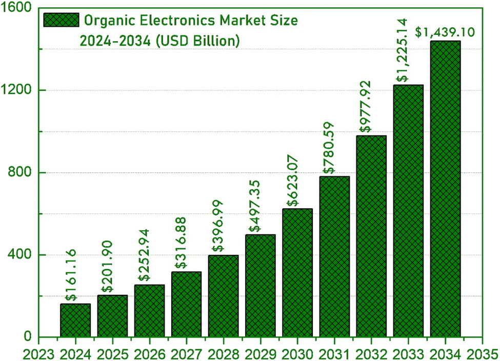 | ||
| Fig. 10 Organic electronics market size (USD billion) and forecast 2024 to 2034. | ||
Currently, effort is concentrated on improving organic materials to be more stable as well as to function to a higher degree under different environmental conditions. Therefore, there are emerging partnerships between industry players, researchers, and universities that are designing new materials and integration methods that are tailored to meet the harsh specifications of commercial applications. As the electronics industry continues to advance towards organic technologies, the global economy is poised for a significant shift in innovation and sustainability, with organic electronics likely to play a pivotal role in future technology discussions.
8.5. Biopolymeric and natural-derived materials for sustainable organic electronics
The development of soft and environmentally benign electronic technologies has accelerated interest in renewable biopolymers and natural macromolecules, which are valued not only for their ecological benefits but also for their favorable physicochemical and optoelectronic attributes (Fig. 11). Cellulose, available as thin films or as nanofibrils (CNF) and nanocrystals (CNC), serves as a transparent, smooth, and mechanically robust substrate or dielectric for paper-based and flexible electronic systems. It supports printed conductors, radio-frequency elements, sensors, and chiral photonic architectures.81 Chitosan, a chitin-derived polysaccharide, is processable in aqueous media and functions effectively as a high-capacitance dielectric and ionic gel in organic field-effect transistors (OFETs) and bioelectronic platforms, enabling low-voltage operation even on mechanically fragile substrates.82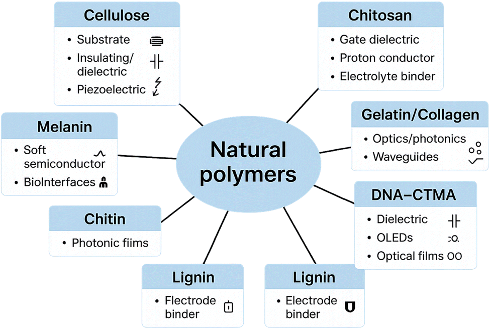 | ||
| Fig. 11 Natural polymers and typical roles in electronics/photonics. | ||
Silk fibroin, obtained from silkworm cocoons, produces ultra-smooth, transparent films suitable for optical and photonic structures such as waveguides, microcavities, and encapsulation coatings with high biocompatibility.83 DNA-CTMA (cetyltrimethylammonium) complexes form optically clear (n ≈ 1.5), low-loss interlayers employed as insulating or spacing layers and as host matrices in organic light-emitting diodes (OLEDs) and random-laser systems.84 Furthermore, melanin and its synthetic analogue, polydopamine, exemplify multifunctional organic semiconductors that enable simultaneous ionic, protonic, and electronic conduction, making them particularly suitable for neuromorphic and biointerface devices.85
Despite these advantages, the use of biopolymers demands precise control of environmental and processing parameters, such as humidity, oxygen exposure, pH, and drying conditions, to ensure stability and reproducibility. Collectively, cellulose, chitosan, silk fibroin, DNA-CTMA, and melanin constitute a mature and complementary class of renewable materials that can extend or even replace synthetic polymers in sustainable soft electronics, iontronic systems, and biocompatible photonic technologies.86
The integration of such biopolymers into organic electronic architectures represents a paradigm shift toward eco-efficient and transient technologies. Materials including cellulose (and its nanostructured derivatives), chitosan, silk fibroin, gelatin, starch-based polymers, and polylactic acid (PLA) offer intrinsic advantages such as renewability, biodegradability, biocompatibility, and mechanical compliance, making them promising substrates, dielectrics, encapsulants, and scaffold matrices for flexible and disposable devices (Fig. 12).87
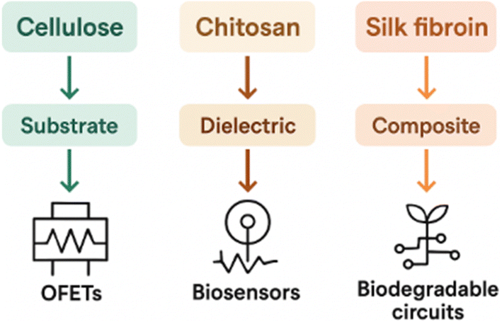 | ||
| Fig. 12 Biopolymer integration pathways in sustainable organic electronics. | ||
Cellulose nanofibers provide a unique combination of high transparency, low surface roughness, and mechanical strength, suitable for transparent substrates and thin semiconductor coatings.88 Chitosan's proton-conducting nature and chemical functionality enable efficient low-voltage gating and improved interfacial adhesion. Silk fibroin stands out for implantable electronics due to its favorable dielectric properties, mechanical stability, and controllable biodegradation rate. Composite formulations combining these polymers with conductive fillers such as PEDOT:PSS, graphene, carbon nanotubes, or metallic nanowires create percolative networks that enhance electrical performance while retaining environmental benefits.
Chemical modification and blending strategies allow fine-tuning of hydrophilicity, processability, and mechanical modulus, key factors for integrating biopolymers with conventional organic semiconductors and scalable printing methods. Nevertheless, challenges persist, including moisture sensitivity, limited thermal stability, and variability in raw material purity. Overcoming these issues requires targeted molecular engineering, surface functionalization, and the development of low-temperature, green processing routes.
Overall, biopolymeric systems such as cellulose, chitosan, silk fibroin, DNA-CTMA, and melanin represent a promising class of renewable materials capable of complementing or replacing synthetic polymers in soft, sustainable electronics, iontronics, and biophotonic technologies.89,90
8.6. End-of-life management and circular strategies in organic electronics
A credible sustainability narrative for organic electronics must extend beyond low-energy fabrication and renewable feedstocks to encompass end-of-life (EoL) management.91 Responsible EoL pathways include mechanical reuse, solvent- or catalyst-driven chemical recycling, controlled biodegradation for transient devices, and design for disassembly that facilitates material recovery. Each route has distinct technical and environmental trade-offs that must be considered in life-cycle assessments (LCAs).Chemical recycling, selective depolymerization of conjugated polymers into monomers or oligomers under mild catalytic or solvothermal conditions, offers a route to recover molecular building blocks for re-polymerization, thereby closing material loops. Solvent recovery systems integrated into solution-processing lines can markedly reduce volatile organic compound (VOC) emissions and solvent consumption; implementing solvent recycling is therefore a high-impact intervention for reducing the cradle-to-gate footprint of printed organic electronics. For single-use or implantable applications, eco-dissolvable or water-soluble encapsulation layers permit controlled device disintegration, simplifying disposal and minimizing persistent electronic waste (Fig. 13).
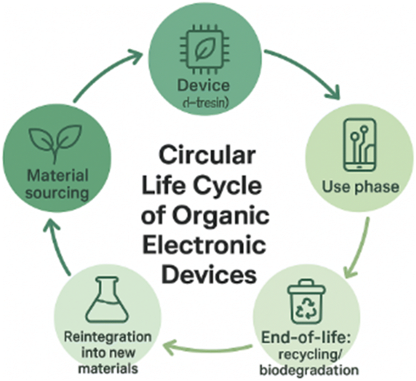 | ||
| Fig. 13 Circular life cycle of organic electronic devices. | ||
LCAs applied to printed organic devices consistently highlight hotspots such as solvent usage, electrode materials (e.g., rare metals or heavy-metal inks), and non-degradable encapsulants. Consequently, pragmatic priorities are: (i) substituting hazardous solvents with greener alternatives or adopting solvent-free deposition techniques (e.g., dry transfer, vapor deposition where appropriate); (ii) developing bio-derived or carbon-based electrode materials that avoid scarce or toxic constituents; (iii) engineering modular device architectures that enable selective recovery of high-value components; and (iv) incorporating EoL criteria into early materials and device design stages. Complementary policy measures, producer responsibility schemes, standardized EoL testing protocols, and incentives for recycling infrastructure, will be essential to realize circularity at scale. Integrating material innovation with process engineering and policy frameworks thus transforms sustainability from a marketing claim into an operational requirement for industrial deployment.
8.7. Organic, inorganic, and hybrid technologies: opportunities and challenges
A realistic appraisal of the technological landscape positions organic, inorganic and hybrid electronic technologies as complementary rather than mutually exclusive (Fig. 14). Inorganic semiconductors (silicon, III–V compounds, metal-oxides) dominate applications demanding high carrier mobility, thermal robustness and long operational lifetimes.92 Organic semiconductors, by contrast, excel where mechanical flexibility, low-cost solution processing and molecular tunability are decisive, for example, in large-area, wearable, or disposable electronics. Hybrid systems (e.g., organic–inorganic heterostructures, perovskite-polymer blends, or carbon-nanomaterial reinforced polymers) exploit synergistic advantages to improve electrical performance and environmental stability while retaining some degree of flexibility and manufacturability.93,94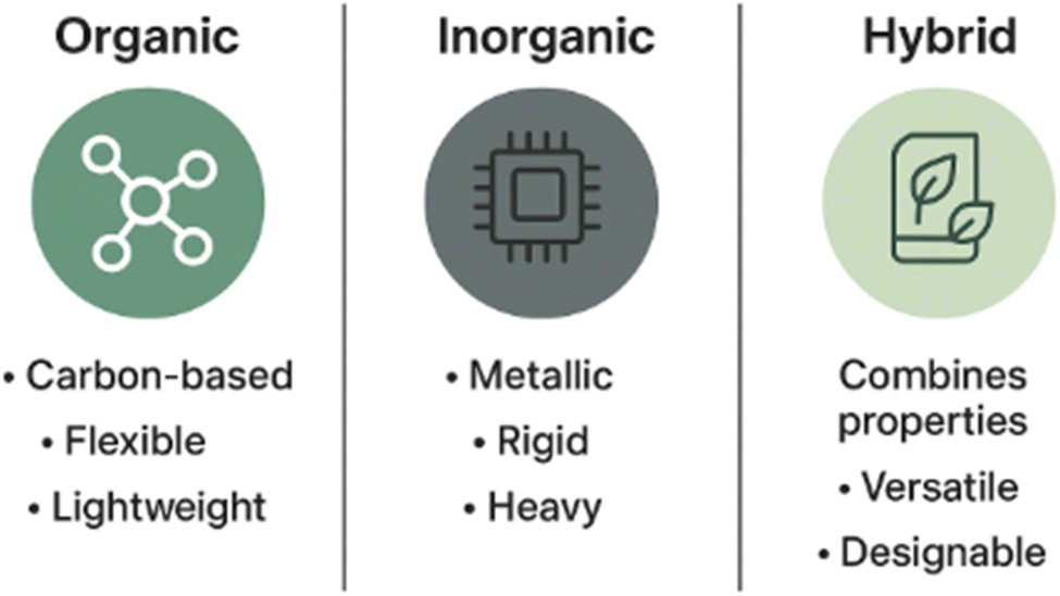 | ||
| Fig. 14 Comparison of organic, inorganic, and hybrid technologies. | ||
From an industrial perspective, the successful market adoption of organic technologies depends on meeting a set of pragmatic requirements: reproducible charge transport characteristics compatible with the target application (including sufficient mobility and on/off ratios for transistor operation), operational stability under relevant environmental stressors (humidity, temperature, mechanical cycling), long-term device lifetimes appropriate for the use case, and compatibility with scalable manufacturing (e.g., roll-to-roll printing, inkjet deposition) with acceptable yield and process control. Additional non-technical factors, material supply chains, standardization of test protocols, packaging and encapsulation solutions, and EoL infrastructure, are equally determinative for commercialization.
Hybrid approaches currently offer the most practical route to bridge the performance gap: inorganic nanostructures or metal oxides can provide high-mobility pathways or robust contacts, while organic matrices confer flexibility and low-temperature processability. Looking forward, continued progress in molecular design, interface engineering, and printable high-performance inks is expected to narrow performance differentials. Nevertheless, rather than supplanting traditional inorganic platforms, organic and hybrid technologies are likely to target niche and emerging markets-wearables, smart packaging, environmental sensors, and biomedical implants, where their unique value propositions (light weight, conformability, disposability, or biodegradability) are decisive. Strategic integration of technical performance targets with environmental and economic constraints will determine which applications are best served by organic, inorganic, or hybrid solutions.
8.8. Comparative performance metrics of representative organic electronic materials
The performance of organic electronic materials is governed by an intricate interplay between molecular structure, processing conditions, and device configuration. Achieving the optimal balance among mechanical robustness, electrical efficiency, and environmental sustainability remains a central challenge in the field. To provide a quantitative and integrative overview, Tables 1 and 2 present the key mechanical-structural and electrical–functional properties of representative material classes employed in contemporary flexible and sustainable electronics. Together, these data delineate the relationships between composition, morphology, and functionality, offering insights into how molecular design strategies influence macroscopic performance.| Material system | Representative example(s) | Tensile strength (MPa) | Elongation at break (%) | Young's modulus (GPa) | Mechanical domain insight |
|---|---|---|---|---|---|
| Conjugated polymer (p-type) | P3HT, DPP-based polymers | 30–50 | 10–30 | 0.4–1.2 | Moderate strength; brittle; improved via copolymerization or blending |
| Conducting polymer blend | PEDOT:PSS | 40–60 | 5–25 | 1.0–2.0 | Stiff but processable; mechanical limits under cyclic bending |
| Elastomeric conjugated copolymer | SEBS–P3HT, stretchable polythiophenes | 10–25 | 100–300 | 0.02–0.1 | Excellent elasticity; ideal for stretchable transistors |
| Biopolymer substrate/dielectric | Cellulose, silk fibroin, chitosan, PLA | 50–150 | 5–80 | 2–5 | High strength and flexibility; suitable for biodegradable supports |
| 3D-printable polymeric ink | PLA-based, polyurethane–PEDOT formulations | 20–60 | 50–200 | 0.1–1 | Tunable mechanical profile; depends on print parameters |
| Material system | Electrical conductivity (S cm−1) | Biodegradability/recyclability | Typical application | Functional domain insight |
|---|---|---|---|---|
| Conjugated polymer (p-type) | 10−5–10−2 | Limited; recyclable via solvent recovery | OFETs, OPVs | High charge transport; limited lifetime |
| Conducting polymer blend | 102–103 | Partially recyclable (aqueous medium) | Electrodes, sensors | Benchmark for conductivity; poor stretchability |
| Elastomeric conjugated copolymer | 10−3–1 | Non-biodegradable, recyclable | Wearable transistors | Balanced conductivity and flexibility |
| Biopolymer substrate/dielectric | 10−7–10−4 | Fully biodegradable | Flexible substrates, transient devices | Low charge mobility; high eco-compatibility |
| Biopolymer–conductor composite | 10−2–101 | Partially biodegradable | Biosensors, eco-electronics | Promising trade-off between performance and sustainability |
| Hybrid nanocomposite | 10–102 | Recyclable (depends on filler) | Flexible circuits | High stability; multi-functional integration |
| 3D-printable polymeric ink | 10−4–10 | Biodegradable or recyclable | Additive-manufactured devices | Adaptable for complex geometries |
Elastomeric conjugated copolymers, exemplified by SEBS-P3HT composites, achieve high extensibility (up to 300%) and low moduli, thus enabling skin-like mechanical compliance desirable for wearable and implantable devices. Conversely, biopolymeric matrices such as cellulose, chitosan, silk fibroin, and polylactic acid (PLA) combine high tensile strength (50–150 MPa) with moderate flexibility and excellent biodegradability, establishing them as sustainable substrates and dielectric components. The emergence of 3D-printable polymeric inks, often formulated from PLA or polyurethane-PEDOT systems, further introduces tunability of mechanical response through controlled printing parameters, offering a route toward structurally customized and mechanically adaptive organic devices.
Biopolymers, although inherently insulating (10−7 to 10−4 S cm−1), offer exceptional eco-compatibility and complete biodegradability, making them valuable for transient or resorbable devices. The formation of biopolymer-conductor composites, where conductive fillers such as carbon nanotubes, graphene, or PEDOT:PSS are embedded within cellulose or chitosan matrices, significantly enhances conductivity (10−2 to 10 S m−1) while maintaining partial biodegradability. These hybrid systems embody a promising compromise between environmental responsibility and electrical performance. Hybrid nanocomposites, incorporating inorganic nanostructures (e.g., metal oxides or carbon allotropes) into organic matrices, combine excellent electrical stability (up to 102 S cm−1) with recyclability and mechanical resilience, thereby representing a viable path toward next-generation, multifunctional flexible circuits.
Finally, 3D-printable inks bridge manufacturing scalability with sustainability, delivering moderate conductivity (10−4 to 10 S cm−1) and biodegradable compositions compatible with additive manufacturing.98 Their processability under mild conditions allows the fabrication of complex architectures for applications ranging from biosensors to soft robotics, where both flexibility and environmental safety are critical.
The comparative analysis in Tables 1 and 2 reveals a performance-sustainability continuum across material classes. Synthetic conjugated polymers dominate in electronic performance but exhibit limited environmental compatibility. Biopolymeric systems are exemplary for biodegradability and mechanical compliance yet lag in charge transport efficiency. Hybrid and composite systems occupy a pivotal middle ground, achieving synergy between performance and sustainability.
Future research should prioritize molecularly engineered hybrid frameworks that combine ordered π-conjugated domains for efficient transport with degradable or recyclable backbones. Parallel advances in interface engineering, solvent-free processing, and standardized characterization protocols will be essential to establish reproducible benchmarks and enable cross-laboratory comparability. Through these integrated strategies, organic electronics can transition from niche laboratory prototypes to scalable, circular, and environmentally responsible technologies that underpin the next generation of flexible and sustainable electronic systems.
8.9. Emergent manufacturing routes: nanocomposites and additive fabrication
The continuous drive toward sustainable, high-performance, and scalable production has catalyzed the integration of nanocomposite engineering with additive manufacturing (AM) techniques in organic electronics.99 These two approaches, acting synergistically, enable precise control over microstructure, morphology, and composition, while markedly reducing energy consumption and waste compared to conventional photolithographic or vacuum-based processing.Interfacial engineering is critical in this context: surface functionalization of nanoparticles with π-conjugated or polar moieties improves compatibility with the polymeric matrix and prevents agglomeration, ensuring homogeneous electronic pathways. Beyond electrical enhancement, nanocomposite architectures also impart thermal stability, optical tunability, and self-healing capability, making them ideal for flexible displays, thermally stable sensors, and energy-harvesting modules. The development of green synthesis routes, such as aqueous exfoliation or bio-based surfactant stabilization, further aligns nanocomposite fabrication with circular-economy principles.
Emergent 3D-printable inks based on biodegradable matrices (e.g., PLA, cellulose acetate, chitosan) doped with conductive nanofillers bridge electronic functionality with environmental compatibility. Such formulations allow fabrication of fully printed transistors, stretchable interconnects, OLEDs, and biosensors with hierarchical architectures and locally tunable mechanical compliance. Multi-material AM enables spatially graded structures where electronic, dielectric, and elastomeric regions coexist, mimicking biological tissue flexibility while maintaining robust electrical continuity.
The confluence of nanocomposite design and additive manufacturing heralds a new manufacturing paradigm for organic electronics, one highlighting programmable architectures, recyclability, and functional integration.102 Through digitally guided deposition and nanoscale structuring, devices can be fabricated with site-specific performance, self-healing behavior, and end-of-life biodegradability. Remaining challenges include ensuring long-term interfacial stability, mastering cross-scale modeling of structure–property–process relationships, and standardizing AM protocols for reproducible device performance.
Future directions will likely merge machine-learning-driven ink formulation, in situ diagnostics during printing, and closed-loop material recycling, establishing additive nanomanufacturing as the cornerstone of a sustainable organic-electronics industry. This emerging technological synergy thus not only advances device efficiency and mechanical adaptability but also redefines how electronic materials are conceived, processed, and reintegrated into the ecological cycle.
9. Nonlinear optical organic materials in electronic applications
Organic materials exhibiting nonlinear optical (NLO) behavior have garnered considerable attention due to their pivotal role in advanced photonic and optoelectronic technologies. These materials offer key advantages such as molecular design flexibility, ultrafast response times, and compatibility with solution-processable techniques, making them particularly attractive for applications in frequency doubling, electro-optic modulation, optical switching, and data storage.103–105 Their integration into electronic architectures complements the broader scope of organic electronics, reinforcing the multifunctionality and adaptability of carbon-based systems.The nonlinear response in organic molecules arises from the electronic polarization under intense electromagnetic fields, and is quantified by hyperpolarizabilities, first-order (β) for second-order NLO effects and second-order (γ) for third-order phenomena.106 High NLO activity is typically achieved in π-conjugated systems exhibiting strong intramolecular charge transfer (ICT), which is most effective in molecules with a donor–π–acceptor (D–π–A) configuration. This molecular architecture facilitates efficient delocalization of electrons, resulting in large dipole moment differences between the ground and excited states, an essential condition for enhancing optical nonlinearities.107
Notable classes of organic NLO materials include push–pull chromophores such as stilbenes, azobenzenes, chalcones, and Schiff bases,108,109 as well as conjugated polymers like poly(p-phenylenevinylene) (PPV), polythiophenes, and polyfluorenes.110 These systems benefit from planarity, extended conjugation, and structural modularity. Additionally, metal–organic hybrids, such as transition-metal-coordinated donor–acceptor complexes, offer enhanced photostability and broadened absorption spectra, contributing to improved NLO performance.111
Theoretical approaches, particularly those based on density functional theory (DFT) and time-dependent DFT (TD-DFT), have become instrumental in predicting and optimizing NLO properties.112–116 These computational methods enable the evaluation of frontier molecular orbitals, dipole moments, and hyperpolarizability tensors, facilitating rational design prior to synthesis. Experimental validation using techniques such as EFISH (electric-field-induced second harmonic) and Z-scan confirms the strong NLO responses of many candidate molecules.117,118
Despite these advances, translating high intrinsic NLO activity into functional devices remains challenging due to morphological instability, film-processing limitations, and photodegradation under continuous illumination.119 To address these issues, strategies such as incorporating NLO chromophores into polymer matrices, forming self-assembled monolayers, or embedding them in sol–gel hybrid systems have shown promise in improving orientation control, film-forming ability, and environmental robustness.120
The strategic incorporation of NLO-active organic materials into flexible and printable electronic platforms opens new avenues in integrated photonics, wearable optical sensors, and next-generation optical computing. Their synergy with organic electronic components such as OFETs and OLEDs strengthens the case for organic systems as a comprehensive platform for multifunctional, sustainable, and high-performance optoelectronics. Continued advancements in synthesis, molecular modeling, and device integration are expected to drive the development of tailored NLO materials, ultimately enabling compact, lightweight, and energy-efficient photonic technologies.
10. Conclusion
Organic electronics has matured into a pivotal interdisciplinary field bridging molecular chemistry, materials science, and device engineering, enabling the creation of lightweight, flexible, and energy-efficient systems that redefine the architecture and sustainability of modern technologies. Through advances in conjugated polymers, organic semiconductors, and hybrid nanocomposites, researchers have established a versatile materials platform capable of competing with, and complementing, conventional inorganic counterparts.The field has progressed from laboratory demonstrations to pre-industrial implementations, driven by improved understanding of structure–property–function correlations and the development of scalable processing techniques. The integration of biopolymeric and naturally derived materials, such as cellulose, chitosan, and polylactic acid, marks a paradigm shift toward environmentally responsible and biodegradable device architectures, aligning performance optimization with ecological imperatives. Complementarily, the incorporation of end-of-life management frameworks and life-cycle assessment (LCA) methodologies transforms sustainability into a measurable engineering parameter rather than a conceptual ideal.
The emergence of nanocomposite engineering and additive manufacturing (AM) has further revolutionized the fabrication of organic devices. By enabling digital, low-temperature, and solvent-efficient production, these approaches support circular manufacturing paradigms and the customization of device architectures with unprecedented precision. This technological convergence not only enhances charge transport, mechanical resilience, and optical tunability but also ensures compatibility with recyclable or biodegradable feedstocks.
Looking forward, the frontier of organic electronics lies in the rational coupling of molecular design, process optimization, and artificial-intelligence-driven materials discovery. The integration of nonlinear optical (NLO) organic systems into flexible photonic platforms and the deployment of hybrid organic-inorganic architectures will expand functional versatility and performance thresholds. Achieving long-term operational stability, establishing standardized characterization protocols, and developing closed-loop recycling infrastructures will be critical for the transition from proof-of-concept devices to sustainable commercial applications.
Ultimately, organic electronics embodies a transformative technological and societal endeavor: it not only redefines electronic materials in terms of flexibility and efficiency but also reshapes how technology interacts with the environment. The convergence of high-performance design and ecological stewardship positions this field as a cornerstone of next-generation, sustainable and circular electronic innovation.
Authors information regarding figures
All figures included in this manuscript were either independently redrawn by the authors or generated using artificial intelligence (AI) tools under the authors' direct supervision. No copyrighted material has been reproduced from previously published sources. Certain schematic representations were conceptually inspired by established scientific literature but have been fully entirely re-illustrated to ensure both originality and full compliance with copyright and publication ethics.Conflicts of interest
There are no conflicts to declare.Data availability
The data underlying this study are available in the published article.References
- Organic Electronics: Materials, Manufacturing and Applications, ed. H. Klauk, Wiley-VCH, Weinheim, 2006, ISBN 9783527312641 Search PubMed.
- P. Samori and F. Cacialli, Functional Supramolecular Architectures: for Organic Electronics and Nanotechnology, Wiley, 2010, ISBN 978-3-527-32611-2 Search PubMed.
- Electronique Organique, ed. T. Grasser, G. Meller and M. Baldo, Springer, Heidelberg, 2010, ISBN 978-3-642-04537-0 Search PubMed.
- H. S. Nalwa, Handbook of Organic Electronics and Photonics, American Scientific Publishers, 2008, vol. 3, ISBN 1-58883-095-0 Search PubMed.
- J. B. Kaushal, P. Raut and S. Kumar, Organic Electronics in Biosensing: A Promising Frontier for Medical and Environmental Applications, Biosensors, 2023, 13(11), 976, DOI:10.3390/bios13110976.
- J. Tarver, J. E. Yoo and Y.-L. Loo, Organic Electronic Devices with Water-Dispersible Conducting Polymers, in Comprehensive Nanoscience and Technology, 2011, vol. 4, pp. 413–446 Search PubMed.
- J. Wan, et al. Applications of organic solar cells in wearable electronics, Wearable Electron., 2024, 1, 26–40 CrossRef CAS.
- S. E. George, et al. Exploring the photophysical, electrochemical and excited state dynamics of 2, 8-disubstituted dibenzothiophene oligomers for organic electronics: Theoretical and experimental insights, J. Mol. Struct., 2025, 1326, 141116, DOI:10.1016/j.molstruc.2024.141116.
- W. Khelifi, et al. Recent developments in indacenodithiophene and indacenodithienothiophene-based donor-acceptor conjugated polymers: From design to device performance in Organic electronics, Prog. Polym. Sci., 2024, 151, 101804, DOI:10.1016/j.progpolymsci.2024.101804.
- V. Bhat, et al. Computational approaches for organic semiconductors: from chemical and physical understanding to predicting new materials, Chem. Rev., 2023, 123(12), 7498–7547, DOI:10.1021/acs.chemrev.2c00704.
- L. Ding, et al. Polymer Semiconductors: Synthesis, Processing, and Applications, Chem. Rev., 2023, 123(12), 7421–7497, DOI:10.1021/acs.chemrev.2c00696.
- F. H. Abd Nasir, et al. Charge carrier trapping in organic semiconductors: Origins, impact and strategies for mitigation, Synth. Met., 2024, 307, 117661, DOI:10.1016/j.synthmet.2024.117661.
- W. Zhao, S. Cao, H. Cai, Y. Wu, Q. Pan, H. Lin, J. Fang, Y. He, H. Deng and Z. Liu, Chitosan/silk fibroin biomimic scaffolds reinforced by cellulose acetate nanofibers for smooth muscle tissue engineering, Carbohydr. Polym., 2022, 298, 120056, DOI:10.1016/j.carbpol.2022.120056.
- S. Shaji, A. Anna, S. Kiran, A. Aboobaker, A. J. Varghese, P. Nancy, L. Ravindran and S. Thomas, Review on sustainable flexible electronics: exploring the potential of chitosan, cellulose starch, silk fibroin and gelatin, Discov. Polym., 2025, 2, 19, DOI:10.1007/s44347-025-00031-7.
- M. Maturi, V. Vetri Buratti, G. Casula, E. Locatelli, L. Sambri, A. Bonfiglio and M. Comes Franchini, Surface-Stabilization of Ultrathin Gold Nanowires for Capacitive Sensors in Flexible Electronics, ACS Appl. Nano Mater., 2021, 4(9), 8668–8673, DOI:10.1021/acsanm.1c01849.
- H. Shirakawa, E. J. Louis, A. G. MacDiarmid, C. K. Chiang and A. J. Heeger, Synthesis of electrically conducting organic polymers: Halogen derivatives of polyacetylene, (CH)x, J. Chem. Soc. Chem. Commun., 1977, 578, 10.1039/c39770000578 16.
- H. Shirakawa, The discovery of polyacetylene film, Synth. Met., 2001, 125, 3–10, DOI:10.1016/S0379-6779(01)00507-0.
- A. Heeger, Electrical Conductivity in Doped Polyacetylene, Phys. Rev. Lett., 1977, 39, 1098, DOI:10.1103/PhysRevLett.39.1098.
- H. Shirakawa, E. J. Louis, A. G. MacDiarmid, C. K. Chiang and A. J. Heeger, Synthesis of electrically conducting organic polymers: Halogen derivatives of polyacetylene, (CH)x, J. Chem. Soc. Chem. Commun., 1977, 578, 10.1039/C39770000578 16.
- K. T. Kamtekar, A. P. Monkman and M. R. Bryce, Recent Advances in White Organic Light-Emitting Materials and Devices (WOLEDs), Adv. Mater., 2010, 22(5), 572–582, DOI:10.1002/adma.200902148.
- A. Salleo, M. L. Chabinyc, M. S. Yang and R. A. Street, Polymer thin-film transistors with chemically modified dielectric interfaces, Appl. Phys. Lett., 2002, 81(23), 4383–4385, DOI:10.1063/1.1527691.
- J. Nelson, Polymer:fullerene bulk heterojunction solar cells, Mater. Today, 2011, 14(10), 462–470, DOI:10.1016/S1369-7021(11)70210-3.
- T. Xia, Y. Cai, H. Fu and Y. Sun, Optimal bulk-heterojunction morphology enabled by fibril network strategy for high-performance organic solar cells, Sci. China Chem., 2019, 62(6), 662–668, DOI:10.1007/s11426-019-9478-2.
- J. Nelson, Organic photovoltaic films, Mater. Today, 2002, 5(5), 20–27, DOI:10.1016/S1369-7021(02)05532-3.
- M. Urien, L. Bailly, L. Vignau, E. Cloutet, A. De Cuendias, G. Wantz, H. Cramail, L. Hirsch and J.-P. Parneix, Effect of the regioregularity of poly(3-hexylthiophene) on the performance of organic photovoltaic devices, Polym. Int., 2008, 57(5), 764–769, DOI:10.1002/pi.2407.
- M. Bouachrine and T. Lakhlifi, Optimization of the electrosynthesis of the poly3-n-hexylthiophene, J. Chim. Phys., 1998, 95(5), 987–1000, DOI:10.1051/jcp:1998226.
- S. M. Bouzzine, S. Bouzakraoui, M. Hamidi and M. Bouachrine, Impact of the torsion on the optoelectronic properties of poly(3-alkylthiophene): a spectroscopic and theoretical approach, Asian J. Chem., 2007, 19, 1651–1657 CAS.
- P. Vanlaeke, A. Swinnen, I. Haeldermans, G. Vanhoyland, T. Aernouts, D. Cheyns, C. Deibel, J. D'Haen, P. Heremans, J. Poortmans and J. V. Manca, P3HT/PCBM bulk heterojunction solar cells: Relation between morphology and electro-optical characteristics, Sol. Energy Mater. Sol. Cells, 2006, 90(14), 2150–2158, DOI:10.1016/j.solmat.2006.02.010.
- K. Bednarczyk, W. Matysiak, T. Tański, H. Janeczek, E. Schab-Balcerzak and M. Libera, Effect of polyaniline content and protonating dopants on electroconductive composites, Sci. Rep., 2021, 11, 7487, DOI:10.1038/s41598-021-86950-4.
- J. C. Chiang and A. G. MacDiarmid, 'Polyaniline': Protonic Acid Doping of the Emeraldine Form to the Metallic Regime, Synth. Met., 1986, 1(13), 193, DOI:10.1016/0379-6779(86)90070-6.
- A. G. MacDiarmid, S. K. Manohar, J. G. Masters, Y. Sun, H. Weiss and A. J. Epstein, Polyaniline: Synthesis and properties of pernigraniline base, Synth. Met., 1991, 41(1–2), 621–626, DOI:10.1016/0379-6779(91)91145-Z.
- Z. A. Boeva and V. G. Sergeyev, Polyaniline: Synthesis, properties, and application, Polym. Sci., Ser. C, 2014, 56(1), 144–153, DOI:10.1134/S1811238214010032.
- G. Mloston, Heterocycles in materials chemistry, Chem. Heterocycl. Compd., 2017, 53(1), 1–6, DOI:10.1007/s10593-017-2013-0.
- T. Torroba, O. A. Rakitin and C. W. Rees, New heterocyclic materials, in Proceedings of the 4th International Electronic Conference on Synthetic Organic Chemistry, MDPI, Basel, Switzerland, 2000, pp. 1–30, DOI:10.3390/ecsoc-4-01781.
- M. Maturi, L. Migliorini, S. M. Villa, T. Santaniello, F.-D. Natalia, S. Ignacio Molina, P. Milani, A. Sanz de León and M. Comes Franchini, 3D-Printing of Highly Piezoelectric Barium Titanate Polymer Nanocomposites with Surface-Modified Nanoparticles at Low Loadings, Adv. Funct. Mater., 2025, 35(1), 2407077, DOI:10.1002/adfm.202407077.
- G. Inzelt. Chapter 1: Introduction, in Conducting Polymers: A New Era in Electrochemistry. Monographs in Electrochemistry, ed. F. Scholz, Springer, 2008, pp. 1–6, ISBN 978-3-540-75929-4 Search PubMed.
- Conducting Polymers, ed. T. Fernandez Otero, Royal Society of Chemistry, Cambridge, 2016, 10.1039/9781782623748, https://pubs.rsc.org/en/content/ebook/978-1-78262-374-8.
- D. Vosgueritchian, M. Tee, J. A. Bolander and Z. Bao, Electronic Properties of Transparent Conductive Films of PEDOT: PSS on Stretchable Substrates, Chem. Mater., 2012, 24(2), 373–382, DOI:10.1021/cm203216m.
- C. I. Simionescu and V. Percec, Progress in polyacetylene chemistry, Prog. Polym. Sci., 1982, 8(1–2), 133–214, DOI:10.1016/0079-6700(82)90009-0.
- Y. Chen, Y. Xie, X. Yan, M. L. Cohen and S. Zhang, Topological carbon materials: A new perspective, Phys. Rep., 2020, 868, 1, DOI:10.1016/j.physrep.2020.05.003.
- L. Groenendaal, F. Jonas, D. Freitag, H. Pielartzik and J. R. Reynolds, Poly(3,4-ethylenedioxythiophene) and Its Derivatives: Past, Present, and Future, Adv. Mater., 2000, 12(7), 481–494, DOI:10.1002/(SICI)1521-4095.
- P. Sakunpongpitiporn, K. Phasuksom, N. Paradee and A. Sirivat, Facile synthesis of highly conductive PEDOT: PSS via surfactant templates, RSC Adv., 2019, 9(11), 6363–6378, 10.1039/C8RA08801B.
- J. Y. Kim, J. H. Jung, D. E. Lee and J. Joo, Enhancement of electrical conductivity of poly(3,4-ethylenedioxythiophene)/poly(4-styrenesulfonate) by a change of solvents, Synth. Met., 2002, 126(2–3), 311–316, DOI:10.1016/S0379-6779(01)00576-8.
- G. Cao, S. Cai, Y. Chen, D. Zhou, H. Zhang and Y. Tian, Facile synthesis of highly conductive and dispersible PEDOT particles, Polymer, 2022, 252, 124952, DOI:10.1016/j.polymer.2022.124952.
- H. Akamatu, K. Inokuchi and K. Matsunage, Organic Semiconductors with High Conductivity. 1. Complexes Between Polycyclic Aromatic Hydrocarbons and Halogens, Bull. Chem. Soc. Jpn., 1956, 29(2), 213, DOI:10.1246/bcsj.29.213.
- C. W. Tang and S. A. Van Slyke, Organic Luminescent Diodes, Appl. Phys. Lett., 1987, 51(12), 913, DOI:10.1063/1.98799.
- J. H. Burroughes, D. D. Bradley, A. R. Brown, R. N. Marks, K. Mackay and R. H. Friend, et al. Light-emitting diodes based on conjugated polymers, Nature, 1990, 348(6293), 539, DOI:10.1038/347539a0.
- B. Forrest, D. Bradley and J. Thompson, Measuring the efficiency of organic light-emitting devices, Adv. Mater., 2003, 15(13), 1043, DOI:10.1002/adma.200302151.
- K. Walzer, B. Maennig and A. Pfeifer, Highly efficient organic devices based on electrically doped transport layers, Chem. Rev., 2007, 107(4), 1233–1271, DOI:10.1021/cr050156n.
- E. W. Godly and R. Taylor, Nomenclature and Terminology of Fullerenes, Pure Appl. Chem., 1997, 69(7), 1411–1434, DOI:10.1351/pac199769071411.
- E. A. Katz, Fullerene Thin Films as Photovoltaic Material, in Nanostructured Materials for Solar Energy Conversion, ed. T. Sōga, Elsevier, 2006, pp. 372–381, ISBN 978-0-444-52844-5 Search PubMed.
- C. Huang, S. Barlow and S. Marder, Perylene-3,4,9,10-tetracarboxylic Acid Diimides: Synthesis, Physical Properties, and Use in Organic Electronics, J. Org. Chem., 2011, 76, 2386–2407, DOI:10.1021/jo2001963.
- B. A. Jones, M. J. Ahrens, M.-H. Yoon, A. Facchetti, T. J. Marks and M. R. Wasielewski, Electron transport: High-mobility air-stable n-type semiconductors with processing versatility: dicyanoperylene-3,4:9,10-bis(dicarboximides), Angew. Chem., Int. Ed., 2004, 43, 6363–6636, DOI:10.1002/ange.200461324.
- T. Khanna, S. Konwar, S. Saloni, S. N. F. Yusuf, P. K. Singh and G. Durga, Structural and optoelectronic analysis of a novel perylene diimide as a light-harvesting material for dye-sensitized solar cells, Curr. Appl. Phys., 2025, 73, 127–135, DOI:10.1016/j.cap.2025.03.006.
- M.-J. Kho, T. Javed, R. Mark, E. Maier and C. David, Final Report: OLED Solid State Lighting: Kodak European Research. MOTI (Management of Technology and Innovation) Project, Judge Business School of the University of Cambridge and Kodak European Research. Final Report presented on 4 March 2008 at Kodak European Research, Cambridge Science Park, Cambridge, UK, 2008.
- R. Konieczny, Own Work, CC BY-SA 3.0, 2006, available at: https://commons.wikimedia.org/w/index.php?curid=1951888 Search PubMed.
- T. Granier, E. L. Thomas, D. R. Gagnon, F. E. Karasz and R. W. Lenz, Structure investigation of poly(p-phenylene vinylene), J. Polym. Sci., Part B: Polym. Phys., 1986, 24(12), 2793–2804, DOI:10.1002/polb.1986.090241214.
- J. H. Burroughes, D. D. Bradley, A. R. Brown, R. N. Marks, K. Mackay and R. H. Friend, et al. Light-emitting diodes based on conjugated polymers, Nature, 1990, 347(6293), 539–541, DOI:10.1038/347539a0.
- A. Salleo, M. L. Chabinyc, M. S. Yang and R. A. Street, Polymer thin-film transistors with chemically modified dielectric interfaces, Appl. Phys. Lett., 2002, 81(23), 4383–4385, DOI:10.1063/1.1527691.
- A. Tsumura, H. Koezuka and T. Ando, Macromolecular electronic device: Field-effect transistor with a polythiophene thin film, Appl. Phys. Lett., 1986, 49(18), 1210–1212, DOI:10.1063/1.97417.
- Material scientist, Own Work, CC BY-SA 3.0, 2019, available at: https://commons.wikimedia.org/w/index.php?curid=9475642 Search PubMed.
- S. Tiwari, A. K. Singh, L. Joshi, P. Chakrabarti, W. Takashima, K. Kaneto and R. Prakash, Poly-3-hexylthiophene based organic field-effect transistor: Detection of low concentration of ammonia, Sens. Actuators, B, 2012, 171–172, 962–968, DOI:10.1016/j.snb.2012.06.010.
- E. K. Solak and E. Irmak, Advances in organic photovoltaic cells: a comprehensive review of materials, technologies, and performance, RSC Adv., 2023, 13, 12244–12269, 10.1039/D3RA01454A.
- H. Zhang, Y. Liu and M. Zhang, Organic Batteries: From Fundamental Principles to Practical Applications, J. Power Sources, 2018, 382, 115–126 CrossRef.
- T. I. Serrano-Arévalo, R. Ochoa-Barragán, C. Ramírez-Márquez, M. El-Halwagi, N. Abdel Jabbar and J. M. Ponce-Ortega, Energy Storage: From Fundamental Principles to Industrial Applications, Processes, 2025, 13(6), 1853, DOI:10.3390/pr13061853.
- K. T. Kamtekar, A. P. Monkman and M. R. Bryce, Recent Advances in White Organic Light-Emitting Materials and Devices (WOLEDs), Adv. Mater., 2010, 22(5), 572–582, DOI:10.1002/adma.200902148.
- B. W. D'Andrade and S. R. Forrest, White Organic Light-Emitting Devices for Solid-State Lighting, Adv. Mater., 2004, 16(18), 1585–1595, DOI:10.1002/adma.200400684.
- Y.-L. Chang and Z.-H. Lu, White Organic Light-Emitting Diodes for Solid-State Lighting, J. Disp. Technol., 2013, 9, 459, DOI:10.1109/JDT.2013.2248698.
- GoPhotonics, 2025, available at: https://www.gophotonics.com/.
- M. Crawford, LEDs for Solid-State Lighting: Performance Challenges and Recent Advances, IEEE J. Sel. Top. Quantum Electron., 2009, 15(4), 1028–1040, DOI:10.1109/jstqe.2009.2013476.
- P. F. Smet, A. B. Parmentier and D. Poelman, Selecting Conversion Phosphors for White Light-Emitting Diodes, J. Electrochem. Soc., 2011, 158(6), R37, DOI:10.1149/1.3568524.
- H.-S. Koo, M. Chen and P.-C. Pan, LCD-based color filter films fabricated by a pigment-based colorant photo resist inks and printing technology, Thin Solid Films, 2006, 515(3), 896–901, DOI:10.1016/j.tsf.2006.07.159.
- Université de Cambridge, PHOTONICS Project: Advancing Organic Materials in Photonics, Cambridge University Press, 2020 Search PubMed.
- S. Chang, J. H. Koo, J. Yoo, M. S. Kim, M. K. Choi, D. H. Kim and Y. M. Song, Flexible and stretchable light-emitting diodes and photodetectors for human-centric optoelectronics, Chem. Rev., 2024, 124(3), 768–859, DOI:10.1021/acs.chemrev.3c00548.
- Philips Research, Organic LED Consortium and its Impact on Commercialization of OLED Technology, Philips Electronics, 2021 Search PubMed.
- Renewable Energy Research Institute, OPV4ALL: Innovations in Organic Photovoltaics, Renew. Energy J., 2020, 34(4), 220–235 Search PubMed.
- Global Electronics Review, Trends and Innovations in Organic Electronics, 2022, vol. 15, pp. 56–72, 2 Search PubMed.
- G. Zhang, C. Xie, P. You and S. Li, Introduction to Organic Electronic Devices, 1st edn, 2022, ISBN 978-981-19-6091-8 Search PubMed.
- Markets and Markets, 2025, available at: https://www.marketsandmarkets.com/Market-Reports/organic-electronics-market-144113962.html.
- Precedence Research, 2025, available at: https://www.precedenceresearch.com/organic-electronics-market.
- S. Majumder, S. Moharana and K. H. Kim, Cellulose nano-papers: A comprehensive review of their synthesis methods, applications, and influence on the circular economy, J. Clean. Prod., 2024, 451, 142045, DOI:10.1016/j.jclepro.2024.142045.
- A. S. Sharova, P. Caironi and A. Campana, et al, Chitosan-gated organic transistors printed on ethyl cellulose as a versatile platform for edible electronics and bioelectronics, Nanoscale, 2023, 15(25), 10808–10819, 10.1039/D3NR01051A.
- M. Rodionova, A. Solomonov, A. Kozell and L. Chernyak, U.Shimanovich, Recent Advances in the Development and Use of Silk-Based Biomaterials, Annu. Rev. Mater. Res., 2025, 55, 307–331, DOI:10.1146/annurev-matsci-080423-114451.
- A. Petriş, P. Gheorghe and I. Rău, DNA-CTMA Matrix Influence on Rhodamine 610 Light Emission in Thin Films, Polymers, 2023, 15(14), 3105, DOI:10.3390/polym15143105.
- T. Eom, J. Kim, J. H. Park and S. H. Kim, et al, Multifunctional Natural and Synthetic Melanin for Bioelectronic Applications: A Review, Biomacromolecules, 2024, 25(9), 5489–5511, DOI:10.1021/acs.biomac.4c00494.
- W. Ying, C. Zhou, H. Sun and W. Huang, Paper-based flexible electronic devices: processing, integration, and applications, npj Flexible Electron., 2025, 9, 80, DOI:10.1038/s41528-025-00446-z.
- K. Ghosh, C. J. Singh, M. Srivastava, S. Behera, S. S. Kaushik, A. Samanta and H. Venkatesan, Chapter 5-Biopolymers in Portable Electronics Applications and Case Study Biopolymer-Based Composites for Energy Generation and Storage, 2026, pp. 141–194, DOI:10.1016/B978-0-443-31522-0.00002-6.
- B. Liu, J. Zeng, P. Li, M. Kui, J. Li and K. Chen, Development of flexible nanocellulose-based composites with enhanced hydrophobicity and improved haze for efficient light management in solar cells, Chem. Eng. J., 2024, 498, 155273, DOI:10.1016/j.cej.2024.155273.
- G. Kaur, K. Uisan, K. L. Ong and C. S. Ki Lin, Recent trends in green and sustainable chemistry & waste valorisation: rethinking plastics in a circular economy, Curr. Opin. Green Sustainable Chem., 2018, 9, 30–39, DOI:10.1016/j.cogsc.2017.11.003.
- C. Cecchini, Bioplastics made from upcycled food waste. Prospects for their use in the field of design, J. Des., 2017, 20(sup1), S1596–S1610, DOI:10.1080/14606925.2017.1352684.
- F. Assies, L. Messmann, A. Thorenz and A. Tuma, Life cycle sustainability assessment of substituting fossil based with biogenic materials: A German case study on drinking cups and insulation boxes, J. Ind. Ecol., 2025, 29(5), 1551–1567, DOI:10.1111/jiec.70067.
- S. Morab, M. M. Sundaram and A. Pivrikas, Review on Charge Carrier Transport in Inorganic and Organic Semiconductors, Coatings, 2023, 13(9), 1657, DOI:10.3390/coatings13091657.
- L. Liu, H. Xiao, K. Jin, Z. Xiao, X. Du, K. Yan, F. Hao, Q. Bao, C. Yi, F. Liu, W. Wang, C. Zuo and L. Ding, 4-Terminal Inorganic Perovskite/Organic Tandem Solar Cells Offer 22% Efficiency, Nano-Micro Lett., 2023, 15, 23, DOI:10.1007/s40820-022-00995-2.
- M. H. Mohammadi, M. Eskandari and D. Fathi, Improving the efficiency of perovskite solar cells via embedding random plasmonic nanoparticles: Optical-electrical study on device architectures, Sol. Energy, 2021, 221, 162–175, DOI:10.1016/j.solener.2021.04.038.
- S. E. Root, S. Savagatrup, A. D. Printz, D. Rodriquez and D. J. Lipomi, Mechanical Properties of Organic Semiconductors for Stretchable, Highly Flexible, and Mechanically Robust Electronics, Chem. Rev., 2017, 117(9), 6467–6499, DOI:10.1021/acs.chemrev.7b00003.
- J. Oswald, D. Beretta, M. Stiefel, R. Furrer, A. Romio, M. Daher Mansour, D. Vuillaume and M. Calame, Charge Transport Across Au-P3HT-Graphene van der Waals Vertical Heterostructures, ACS Appl. Mater. Interfaces, 2022, 14(42), 48240–48249, DOI:10.1021/acsami.2c13148.
- M. N. Gueye, A. Carella, F.-V. Jérôme, R. Demadrille and J.-P. Simonato, Progress in understanding structure and transport properties of PEDOT-based materials: A critical review, Prog. Mater. Sci., 2020, 108, 100616, DOI:10.1016/j.pmatsci.2019.100616.
- P. C. Chavan, G. R. Chate and V. R. Malik, Advances and challenges in conductive ink 3D printing for sustainable PCB fabrication: a comprehensive review aligned toward industry 5.0, Mater. Manuf. Processes, 2025, 1–49, DOI:10.1080/10426914.2025.2559616.
- L. Zhang, X. Huang, L. Liu, N. K. A. Nasar, X. Gu, T. P. Davis, X. Rayne Zheng, L. Wang and R. Qiao, Fabrication of Organic/Inorganic Nanocomposites: From Traditional Synthesis to Additive Manufacturing, Adv. Mater., 2025, 37, 2505504, DOI:10.1002/adma.202505504.
- I. Gamiño-Barocio, E. F. Vázquez-Vázquez, Y. M. Hernández-Rodríguez and O. E. Cigarroa-Mayorga, Tuning the Charge Transfer in MWCNTs via the Incorporation of ZnONPs and AgNPs: The Role of Carbon Binding with ZnO/Ag Heterostructures in Reactive Species Formation, Nanomaterials, 2024, 14(18), 1517, DOI:10.3390/nano14181517.
- A. Gohel, M. Gratuze, M. Ketabi and R. Izquierdo, Direct-Write Printing for Flexible and 3D Electronics: Aerosol Jet vs. Micro Dispensing, Micromachines, 2025, 16(8), 931, DOI:10.3390/mi16080931.
- L. Zhou, J. Miller, J. Vezza, M. Mayster, M. Raffay, Q. Justice, Z. Al Tamimi, G. Hansotte, L. Devi Sunkara and J. Bernat, Additive Manufacturing: A Comprehensive Review, Sensors, 2024, 24(9), 2668, DOI:10.3390/s24092668.
- M. Khalid, R. Hussain, A. Hussain, B. Ali, F. Jaleel, M. Imran, M. A. Assiri, M. U. Khan, S. Ahmed, S. Abid, S. Haq, K. Saleem, S. Majeed and C. J. Tariq, Electron Donor and Acceptor Influence on the Nonlinear Optical Response of Diacetylene-Functionalized Organic Materials (DFOMs): Density Functional Theory Calculations, Molecules, 2019, 24(11), 2096, DOI:10.3390/molecules24112096.
- L. K. Zaitri and S. M. Mekelleche, DFT and TD-DFT study on quadratic NLO response and optoelectronic activity in novel Y-shaped imidazole-based push-pull chromophores, J. Mol. Model., 2021, 27, 136, DOI:10.1007/s00894-021-04764-7.
- J. Deb, D. Paul and U. Sarkar, Density Functional Theory Investigation of Nonlinear Optical Properties of T-Graphene Quantum Dots, J. Phys. Chem. A, 2020, 124(7), 1312–1320, DOI:10.1021/acs.jpca.9b10241.
- E. Rtibi and B. Champagne, Density Functional Theory Study of Substitution Effects on the Second-Order Nonlinear Optical Properties of Lindquist-Type Organo-Imido Polyoxometalates, Symmetry, 2021, 13(9), 1636, DOI:10.3390/sym13091636.
- C. G. Liu and X. H. Guan, Redox and photoisomerization switching of the second-order optical nonlinearity of a tetrathiafulvalene derivative of spiropyran across five states: a DFT study, Phys. Chem. Chem. Phys., 2012, 14, 5297–5306, 10.1039/C2CP23293F.
- I. H. Nayyar, A. E. Masunov and S. Tretiak, Comparison of TD-DFT Methods for the Calculation of Two-Photon Absorption Spectra of Oligophenylvinylenes, J. Phys. Chem. C, 2013, 117(35), 18170–18189, DOI:10.1021/jp403981d.
- C. Liu, D. Zhang, M. Gao and S. Liu, DFT studies on second-order nonlinear optical properties of a series of axially substituted bis(salicylaldiminato) zinc(II) Schiff-base complexes, Chem. Res. Chin. Univ., 2015, 31, 597–602, DOI:10.1007/s40242-015-5004-7.
- P. V. Kolinsky, New materials and their characterization for photonic device applications, Opt. Eng., 1992, 31(8), 15–26, DOI:10.1117/12.58844.
- P. Matozzo, A. Colombo, C. Dragonetti, S. Righetto, D. Roberto, P. Biagini, S. Fantacci and D. Marinotto, A chiral bis(salicylaldiminato) zinc(II) complex with second order nonlinear optical and luminescent properties in solution, Inorganics, 2020, 8, 25, DOI:10.3390/inorganics8040025 4.
- P. Gong, L. An, J. Tong, X. Liu, Z. Liang and J. Li, Design of A-D-A-Type Organic Third-Order Nonlinear Optical Materials Based on Benzodithiophene: A DFT Study, Nanomaterials, 2022, 12(20), 3700, DOI:10.3390/nano12203700.
- A. Hedhli, A. Ghabi, H. Ayachi, S. Ayachi and T. Boubaker, Unlocking nonlinear correlations between Mayr's experimental electrophilicity E and DFT-reactivity descriptors: A study of para-X-substituted diethyl benzylidenemalonates, Chem. Eng. J., 2025, 164656, DOI:10.1016/j.cej.2025.164656.
- B. Abdelaziz, S. Bouazizi, B. Gassoumi, S. Patanè and S. Ayachi, DFT and molecular dynamics study of the optical and electronic properties of nitrobenzofurazan-based molecules for photovoltaic and nonlinear optical applications, Mater. Chem. Phys., 2025, 332, 130269, DOI:10.1016/j.matchemphys.2024.130269.
- T. Slama, Z. Mazouz, B. Abdelaziz, S. Bouazizi, I. Cherif, A. Ghabi, B. Gassoumi, H. Kaur, T. Boubaker and S. Ayachi, Multi-faceted spectroscopic, computational, and nonlinear optical characterization of 2-(pyrrolidin-1-yl)-3,5-dinitropyridine, J. Mol. Liq., 2025, 418, 126722, DOI:10.1016/j.molliq.2024.126722.
- B. Abdelaziz, Z. Mazouz, B. Gassoumi, N. E. I. Boukortt, S. Patanè and S. Ayachi, Molecular engineering of D-π-A-type structures based on nitrobenzofurazan (NBD) derivatives for both organic solar cells and nonlinear optical response, J. Mol. Liq., 2024, 395, 123934, DOI:10.1016/j.molliq.2023.123934.
- D. Rezzonico, S.-J. Kwon, H. Figi, O.-P. Kwon, M. Jazbinsek and P. Günter, Photochemical stability of nonlinear optical chromophores in polymeric and crystalline materials, J. Chem. Phys., 2008, 128, 124713, DOI:10.1063/1.2890964.
- Y. Ren, M. Szablewski and G. H. Cross, Waveguide photodegradation of nonlinear optical organic chromophores in polymeric films, Appl. Opt., 2000, 39(15), 2499–2506, DOI:10.1364/AO.39.002499.
- S. Pandey and S. B. Mishra, Sol-gel derived organic–inorganic hybrid materials: synthesis, characterizations and applications, J. Sol-Gel Sci. Technol., 2011, 59, 73–94, DOI:10.1007/s10971-011-2465-0.
- R. J. Twieg, D. M. Burland, M. Jurich, V. Y. Lee, R. Siemens, A. Skumanich, J. I. Thackara, T. Verbeist, W. Volksen, A. Knoesen, R. A. Hill and D. Yankelevich, Stability and performance issues for nonlinear optical chromophores, polymers and devices, MRS Proc., 2011, 392, 15–26, DOI:10.1557/PROC-392-15.
| This journal is © The Royal Society of Chemistry 2025 |