
 Open Access Article
 This Open Access Article is licensed under a Creative Commons Attribution-Non Commercial 3.0 Unported Licence
Zigzag antiferromagnetic property of two-dimensional NiPX3 (X = S/Se) monolayers in their pristine structure and Janus phase†
Juntao Yang *ab,
XuLi Zhanga,
Zecheng Qua,
Qing Mina,
Jian Xiaa,
Hao Shanga,
Shijun Luoa and
Chengrui Wu*a
*ab,
XuLi Zhanga,
Zecheng Qua,
Qing Mina,
Jian Xiaa,
Hao Shanga,
Shijun Luoa and
Chengrui Wu*a
aShiyan Key Laboratory of Quantum Information and Precision Optics, School of Optoelectronic Engineering, and Collaborative Innovation Center for Optoelectronic Technology, Hubei University of Automotive Technology (HUAT), 167 Checheng West Road, Shiyan City, Hubei, People's Republic of China. E-mail: jtyang@huat.edu.cn; crwu@huat.edu.cn
bHubei Key Laboratory of Optical Information and Pattern Recognition, Wuhan Institute of Technology (WIT), Wuhan, 430205, China
First published on 4th July 2025
Abstract
Transition metal phosphorous trichalcogenides TMPX3 (TM = transition metal, X = S/Se) with a variety of spin configurations serve as excellent platforms for studying the magnetic properties of two-dimensional systems. As an antiferromagnetic semiconductor, the coexistence of ferromagnetic and antiferromagnetic couplings between the nearest neighboring metal ions of NiPX3 remains a debatable topic. In this work, the electronic structures and magnetic properties of NiPX3 monolayers in their pristine structure and Janus phase were systemically investigated using first-principles calculations. It was found that the NiPX3 system possessed an indirect band gap in the zigzag antiferromagnetic ground state with a sizable Néel temperature, as estimated by Monte Carlo simulations. Electronic structures and crystal orbital Hamilton population analyses revealed that the zigzag antiferromagnetic ordering was primarily driven by superexchange interactions through p–d hybridization. Meanwhile, the coexistence of ferromagnetic and antiferromagnetic couplings was facilitated through a combination of antibonding and bonding states below the Fermi level. This work provides a new approach to explore the diverse and intriguing magnetic properties of two-dimensional materials.
1. Introduction
Inspired by the pioneer discovery of an intrinsic magnetic order observed in FePS3 monolayer,1,2 transition metal phosphorus trichalcogenides TMPX3 (TM = transition metals such as Cr, Mn, Fe, Co, and Ni; X = S/Se) have served as excellent platforms to explore two dimensional (2D) magnetism in recent years.3 Most TMPX3 crystals exhibit an antiferromagnetic (AFM) behavior, with a Néel temperature (TN) ranging from 82 K to 155 K (ref. 4 and 5); however, some of these crystals, such as MgPS3 and ZnPSe3 (ref. 6), exhibit a paramagnetic property owing to the presence of unfilled or fully filled d electrons in the metal ions. Bulk TMPX3 materials always exhibit a stacking sequence of “ABAB” in C2/m symmetry or “ABC” in R3 space group and are crystallized by van der Waals (vdW) forces with vdW distances ranging from 3.22 to 3.24 Å (ref. 7); therefore, TMPX3 monolayer can be mechanically exfoliated from the bulk phase owing to the weak cleavage energy, which is smaller than 0.36 J m−2 for graphite.8 The TMPX3 monolayer is characterized by a hexagonal honeycomb-like lattice framework formed by TM atoms. Each TM atom is coordinated with six S/Se atoms, which constitute the upper and lower chalcogen layers. These layers are interconnected via P–P pairs. Specifically, the S/Se atoms are sandwiched between P–P pairs both above and below the honeycomb lattice plane. The P–P dimer vertically bisects the center of the hexagonal unit cell, forming a bipyramid-structure of [PX3−]–[PX3].While 2D TMPX3 monolayers typically demonstrate an AFM behavior, the diverse electronic configurations of TM atoms result in diverse magnetic properties and electronic structures. MnPX3 monolayers exhibit a Néel AFM (nAFM, Fig. 1(b)) configuration as direct band gap semiconductors, while FePX3 monolayers usually exhibit a zigzag AFM (zAFM, Fig. 1(b)) ordering as indirect band gap semiconductors; moreover, CuPX3 system displays a paramagnetic metal character.9,10 In particular, multiple Dirac cones are predicated in paramagnetic NiPX3, PdPX3 and PtPX3 (ref. 11) besides ferromagnetic (FM) CrPSe3 monolayers.12 Some strong electron correlations have been experimentally detected, such as the Mott–Hubbard insulation in the NiPX3 (ref. 13) system and observation of a negative charge transfer in the NiPS3 monolayer.14 Magnetic anisotropy energy (MAE) of TMPX3 monolayers also strongly affects their spin dimensions in Ising, XY and Heisenberg models, which have been observed in FePS3, MnPS3 and CoPS3 monolayers,1,15,16 respectively. Currently, 2D TMPX3 systems have attracted considerable attention owing to their fascinating phenomena arising from strong coupling interactions between magnetism and other physical properties. Superconductivity can be driven into some 2D TMPX3, such as FePS3, MnPS3 and NiPSe3, via a pressure-driven spin-crossover.17–19 A giant optical linear dichroism has been observed in FePS3 and NiPSe3 monolayers using magneto-optical spectroscopy,20 while a second harmonic generation can be produced via polarization-resolved electric quadruple contribution in MnPSe3 monolayer.21 Furthermore, strong electron–phonon coupling in FePS3 (ref. 22) and magnon–phonon coupling23 and photon–matter coupling24 in NiPS3 have been directly determined using magneto-Raman spectroscopy, ultrafast spectroscopy and spectroscopic analysis in conjunction with a microscopic theory, respectively.
 | ||
| Fig. 1 (a) Crystal structure of Janus NiPS3/2Se3/2 from top and side views; (a)–(c) indicate the lattice vectors along [100], [010] and [001] directions, respectively. The dashed rhombus marks a primitive unit cell. (b) Four magnetic configurations in 2D hexagonal lattice; spin-up (UP) and spin-down (DOWN) magnetic moments are indicated by red and blue arrows, respectively. | ||
Despite extensive research into their unique magnetic properties, diverse electronic structures, and intriguing electromagnetic couplings of 2D TMPX3 systems, the origin of the zAFM order in some TMPX3 monolayers remains a subject of ongoing debate. Very recently, the magnetic ground states of NiPS3 and FePS3 monolayers have been demonstrated to exhibit a distinct zigzag antiferromagnetic (zAFM) ordering. Specifically, the zAFM state in NiPS3 is primarily determined by the nearest-neighbor (NN) biquadratic exchange interaction, while in FePS3, it results from the competition between ferromagnetic (FM) NN and antiferromagnetic (AFM) third-nearest-neighbor (3NN) exchange interactions.25 A small distortion between TM–TM distance has been predicted to result in an zAFM alignment in FePS3.9,26 To date, the reason for the co-existence of FM and AFM spin orderings between the NN TM atoms in zAFM systems is unclear. Hence a detailed investigation on the electronic structures is imperative to reveal the mechanism of zAFM spin-ordering, where the adjacent TM chains along the zigzag direction exhibit an opposite orientation in 2D TMPX3.
Since chalcogen-substituted NiPS3−xSex (0 ≤ x ≤ 1.3) crystal has been successfully synthesized recently,27 in this work, the magnetic properties of 2D NiPX3 in its pristine structure in conjunction with its Janus phase of NiPS3/2Se3/2 were systemically investigated using first-principles calculations and Monte Carlo (MC) simulations, including the magnetic exchange parameters (J), MAE and Néeel temperature (TN). In addition, the electronic structures combined with crystal orbital Hamilton populations (COHP) and crystal-field splitting were discussed in detail to reveal the magnetic mechanism of zAFM spin ordering.
2 Computational methods
Based on density functional theory (DFT),28 our spin-polarized first-principles calculations were carried out using the Vienna Ab initio simulation package (VASP).29 The ion–electron interactions were characterized using the Perdew–Burke–Ernzerhof (PBE) exchange–correlation potentials within generalized gradient approximation (GGA).30 The GGA+U model was employed to consider the strong electron correlations in 3d orbitals,31 where the effective Hubbard parameter Ueff = U − J encompasses both Coulomb repulsion U and Hund's rule-driven exchange interaction J. Electronic functions were described using the projector augmented wave method.32 Kinetic energy cut-off was set at 500 eV to expand the wave functions into a plane-wave basis. A 20 Å thickness vacuum space was set to avoid interlayer interactions caused by periodic boundary conditions. The convergence criteria were set to be 10−3 eV Å−1 for the force and 10−6 eV for the energy, respectively. The Brillouin zone (BZ) was sampled using the Monkhorst–Pack method with a Γ-centered 24 × 24 × 1 k-mesh.33 The COHP distributions were also employed to understand the chemical bonding using the lobster program based on DFT.34 Phonon dispersion was calculated using the finite displacement method with phonopy program,35 and Nosé–Hoover thermostat method was employed for ab initio molecular dynamics (AIMD) simulations.36,37 TN values were simulated using MC methods based on the Metropolis algorithm with boundary conditions.38,39 Some data related to the pre- and post-processing processes were obtained using the Vesta program40 and VASPKIT package,41 respectively.3. Results and discussion
3.1. Crystal structure and stability of 2D NiPX3 and NiPS3/2Se3/2
The crystal structure of Janus NiPS3/2Se3/2 monolayer with a 60° torsion angle between the upper S and lower Se layers (Fig. 1) has a primitive unit cell containing two formula units. Based on the distinct chalcogen atom arrangements in upper and lower sublayers, the intrinsic NiPX3monolayer belongs to the D3d space group, while the Janus NiPS3/2Se3/2 exhibits a P![[3 with combining macron]](https://www.rsc.org/images/entities/char_0033_0304.gif) 1m symmetry. Some lattice parameters of 2D NiPS3 and NiPSe3 monolayers in the zAFM state are presented in Table 1. The calculated lattice constant value of a was consistent with the corresponding experimental results.42,43 The lengths of P–P and P–X bonds indicated a covalent character in a [PS3]2−–[PSe3]2 anion pair. Owing to the larger atomic radius of Se than that of S, the lattice constant, monolayer thickness and bond length of NiPSe3 were larger than those of NiPS3. The structure of Janus NiPS3/2Se3/2 was also fully optimized, as shown in Table 1. The bond lengths of Ni–X, P–X and P–P were comparable to those of pristine NiPX3, indicating good structural stability of the Janus monolayer.
1m symmetry. Some lattice parameters of 2D NiPS3 and NiPSe3 monolayers in the zAFM state are presented in Table 1. The calculated lattice constant value of a was consistent with the corresponding experimental results.42,43 The lengths of P–P and P–X bonds indicated a covalent character in a [PS3]2−–[PSe3]2 anion pair. Owing to the larger atomic radius of Se than that of S, the lattice constant, monolayer thickness and bond length of NiPSe3 were larger than those of NiPS3. The structure of Janus NiPS3/2Se3/2 was also fully optimized, as shown in Table 1. The bond lengths of Ni–X, P–X and P–P were comparable to those of pristine NiPX3, indicating good structural stability of the Janus monolayer.
| a | h | lNi–S | lNi–Se | lP–P | lP–S | lP–Se | Eg | |
|---|---|---|---|---|---|---|---|---|
| NiPS3 | 5.83 | 3.12 | 2.47 | — | 2.18 | 2.04 | — | 1.72 |
| NiPSe3 | 6.17 | 3.25 | — | 2.58 | 2.20 | — | 2.22 | 1.45 |
| NiPS3/2Se3/2 | 6.00 | 3.18 | 2.48 | 2.58 | 2.19 | 2.05 | 2.21 | 1.42 |
As shown in Fig. 1, four different magnetic configurations, namely, FM, nAFM, zAFM and stripy AFM (sAFM), were considered to determine the magnetic ground state of the NiPX3 and NiPS3/2Se3/2 monolayers. The structures were fully relaxed, and total energy was calculated for each magnetic configuration. The calculated energies followed the sequence of EzAFM < EnAFM < EFM < EsAFM for different Ueff values, as listed in Table 2. Therefore, the pristine NiPX3 and Janus NiPS3/2Se3/2 monolayers were confirmed to be in the zAFM ground state. For the zAFM ordering, each adjacent Ni chain showed an opposite spin orientation along the zigzag direction, while a parallel spin arrangement perpendicular to this direction was displayed in the spin charge density map, as illustrated in Fig. S1.† Here, U = 4.0 eV was chosen for further discussions because at this energy, the calculated TN and band gap of NiPX3 monolayer were quantitatively close to the corresponding experimental values, which will be discussed in Section 3.2.
| Compound | Ueff | EFM | EnAFM | EzAFM | EsAFM | J1 | J2 | J3 | TN |
|---|---|---|---|---|---|---|---|---|---|
| NiPS3 | 1.0 | −98.12 | −98.48 | −98.51 | −98.06 | 7.25 | 0.89 | −49.13 | 384 |
| 2.0 | −96.07 | −96.34 | −94.36 | −96.02 | 5.55 | 0.72 | −32.02 | 299 | |
| 3.0 | −94.17 | −94.37 | −94.39 | −94.13 | 4.22 | 0.55 | −21.84 | 234 | |
| 4.0 | −92.41 | −92.57 | −92.58 | −92.38 | 3.14 | 0.42 | −15.17 | 186 | |
| 5.0 | −90.81 | −90.92 | −90.94 | −90.78 | 2.29 | 0.32 | −10.62 | 145 | |
| 6.0 | −89.35 | −89.43 | −89.44 | −89.32 | 1.60 | 0.24 | −7.40 | 114 | |
| NiPSe3 | 1.0 | −89.31 | −89.68 | −89.73 | −89.25 | 12.22 | 0.12 | −61.78 | 351 |
| 2.0 | −87.13 | −87.42 | −87.47 | −87.09 | 7.59 | −0.46 | −40.42 | 270 | |
| 3.0 | −85.12 | −85.34 | −85.38 | −85.08 | 5.74 | −0.16 | −27.06 | 210 | |
| 4.0 | −83.26 | −83.43 | −83.46 | −83.23 | 4.33 | −0.03 | −18.68 | 160 | |
| 5.0 | −81.56 | −81.69 | −81.71 | −81.53 | 3.21 | 0.04 | −12.94 | 125 | |
| 6.0 | −80.02 | −80.11 | −80.13 | −79.99 | 2.30 | 0.07 | −8.88 | 95 | |
| NiPS3/2Se3/2 | 1.0 | −93.49 | −93.86 | −93.92 | −93.45 | 9.28 | −0.59 | −55.83 | 371 |
| 2.0 | −91.38 | −91.66 | −91.71 | −91.34 | 6.81 | −0.44 | −36.87 | 291 | |
| 3.0 | −89.42 | −89.63 | −89.67 | −89.39 | 5.25 | −0.17 | −24.94 | 230 | |
| 4.0 | −87.61 | −87.77 | −87.81 | −87.58 | 4.00 | −0.03 | −17.30 | 180 | |
| 5.0 | −85.96 | −86.08 | −86.10 | −85.93 | 2.95 | 0.04 | −11.99 | 137 | |
| 6.0 | −84.45 | −84.54 | −84.56 | −84.43 | 2.14 | 0.07 | −8.35 | 110 |
The structural stability of pristine NiPX3 and Janus NiPS3/2Se3/2 monolayers were examined considering the elastic constants, phonon spectra and AIMD for assessing their mechanical, dynamical and thermal performances, respectively. For a hexagonal lattice, the elastic constants Cij (i, j = 1, 2, and 6) were calculated as C = [∂2E/∂ε2]/S, based on the energy-strain method,44 by applying a series of small in-plane strains ε to the monolayers,45 where E is the total energy variation with the lattice area S. As listed in Table 3, the elastic constants of C11 and C12, with C66 = (C11 − C12)/2, satisfy the formulas C11 > 0 and C11C12 − C212 > 0 of Born–Huang criterion,46 demonstrating that pristine NiPX3 and Janus NiPS3/2Se3/2 exhibit good mechanical stability. Young's modulus Y, shear modulus G and Poisson's ratio v were also calculated, as presented in Table 3; the values for NiPS3/2Se3/2 monolayers located between the corresponding values of NiPS3 and NiPSe3, respectively. All the Y values were much smaller than that of graphene as Y = 340 ± 40 N m−1. These results confirmed the mechanical flexibility of NiPX3 monolayers. The phonon spectra are shown in Fig. 2 along with the density of states for each element. All phonon frequencies were positive in the entire energy range for the three monolayers, revealing excellent dynamical stability.47,48 Clearly, Ni, S/Se and P atoms dominated the low-frequency, mid-frequency and high-frequency branches of the phonon spectra, respectively. During AIMD simulations at 300 K, the total energy curve showed small fluctuations in a narrow range for 10 ps. In addition, the 2D lattice remained in a planar structure after each relaxation for the three monolayers, as shown in Fig. 2.
| C11 | C12 | C66 | Y | G | v | |
|---|---|---|---|---|---|---|
| NiPS3 | 93.17 | 22.97 | 35.10 | 87.51 | 35.10 | 0.25 |
| NiPSe3 | 77.36 | 19.12 | 29.12 | 72.64 | 29.12 | 0.25 |
| NiPS3/2Se3/2 | 88.78 | 21.51 | 33.64 | 83.58 | 33.64 | 0.24 |
 | ||
| Fig. 2 Phonon spectra along with density of states and total energy oscillations with side views of the relaxed structures after AIMD simulations for (a) NiPS3, (b) NiPSe3 and (c) NiPS3/2Se3/2. | ||
As a consequence, 2D NiPX3 and NiPS3/2Se3/2 monolayers exhibited good thermal stability at room temperature.
3.2. Magnetic properties of 2D NiPX3 and NiPS3/2Se3/2
The MAE plays a crucial role in stabilizing the long-range magnetic order by preventing spontaneous spin flipping in 2D magnetic materials. Taking the spin–orbit coupling (SOC) effect into account, the MAE was calculated from the energy difference as EMAE = E(100) − E(001), with spin orientations in and out of the monolayer plane. The partial components of MAE from different atoms, i.e. EMAE (Ni) was also calculated. The MAE results of NiPX3 and NiPS3/2Se3/2 monolayers are listed in Table 4. As can be seen, the EMAE was lower for NiPS3, while it was higher for NiPSe3 and NiPS3/2Se3/2 in ab-plane (100) than in c-direction [001]. The calculated MAE results reveal distinct magnetic easy axes for the three monolayers: NiPS3 exhibits an in-plane (ab-plane) easy axis along the a-axis, while NiPSe3 and NiPS3/2Se3/2 show out-of-plane (c-axis) easy axes perpendicular to the ab-plane.27 Furthermore, the absolute EMAE value was larger in the b [010] direction than in the a [100] direction for the three monolayers owing to their zAFM spin configuration. From the partial component of the EMAE, the magnetic anisotropy of NiPS3 was mainly contributed by Ni atoms, whereas, Se atoms dominated the magnetic anisotropy of NiPSe3 and NiPS3/2Se3/2 monolayers.| Compound | Orientation | EMAE | EMAE (Ni) | EMAE (P) | EMAE (S) | EMAE (Se) | Easy axis |
|---|---|---|---|---|---|---|---|
| NiPS3 | (100) | −87 | −82.1 | 0.7 | 12.6 | ab-Plane | |
| (010) | −95 | −52.5 | 0.5 | 1.5 | |||
| NiPSe3 | (100) | 344 | −6.1 | 0.05 | — | 55.3 | (001) |
| (010) | 473 | −17.2 | 10.4 | 81.1 | |||
| NiPS3/2Se3/2 | (100) | 185 | −6.6 | 0.2 | 1.0 | 64.9 | (001) |
| (010) | 369 | −31.2 | 5.6 | −0.5 | 140.6 |
In order to describe the magnetic interactions between Ni2+ ions for these zAFM monolayers, the magnetic exchange parameters were evaluated using the Heisenberg Hamiltonian as follows:9,49
 | (1) |
The specific heat capacity is definded as  where E represents in ternal energy and kB is the Boltzmann constant; TN could be calculated from the second-order phase transition variable Cv curve. Using MC simulations, the critical transition temperature was evaluated in a 32 × 32 superlattice, with spin directions flipped randomly about 2 × 10⁹ steps per loop. The simulated Cv and E curves as a function of temperature are plotted in Fig. 3. Under the condition of Ueff = 4.0 eV, calculated TN values were in good agreement with the experimental results for each pristine NiPX3 monolayer. In particular, TN = 160 K was very close to the experimental value of 155 K (ref. 52) for NiPS3, while TN = 189 K was slightly lower than 212 K, when measured using temperature-dependent molar susceptibility53 for NiPSe3. Notably, the TN of NiPS3 was lower than that of NiPSe3, which is attributed to the stronger magnetic exchange interactions of NiPSe3 than that of NiPS3. Similarly, the TN of Janus NiPS3/2Se3/2 is predicted to be 180 K, which represents an enhancement compared to 160 K for NiPS3 but shows a decrease relative to 189 K for NiPSe3. This feature was consistent with the behavior predicated for Janus MnPS3/2Se3/2 monolayer, where the magnetic exchange interactions were dominated by transition metal elements.54 The TN values for a series of Ueff values were also calculated and are presented in Table 2 for each monolayer. As mentioned above, the TN was much larger than the corresponding experimental value when U > 4.0 eV but much smaller when U < 4.0 eV. These results further confirmed the rationality of selecting U = 4.0 eV for our calculations. Along with the near-room critical temperature, NiPSe3 and NiPS3/2Se3/2 monolayers, which exhibit an out-of-plane magnetization, are suitable for magnetic storage and low-power switching devices, e.g. spin-transfer torque for electrical switching, whereas the in-plane magnetized NiPS3 monolayer is suited for ultrafast spin information processing, e.g. spin-wave logic circuits.55,56
 | ||
| Fig. 3 Specific heat capacity Cv and total energy E with respect to temperature T for 2D (a) NiPS3, (b) NiPSe3 and (c) NiPS3/2Se3/2 calculated using Monte Carlo simulations. | ||
 | ||
| Fig. 4 Band structures of 2D (a) NiPS3, (b) NiPSe3 and (c) NiPS3/2Se3/2. Black arrow points from valence band maxima to conduction band minima. | ||
In order to investigate the electronic structures in detail, the total density of states (DOS) and orbital projected DOS (PDOS) for NiPX3 and NiPS3/2Se3/2 were plotted in Fig. 5(a)–(c). As the NiPX3 system existed in an AFM ground state, the spin-up channel was symmetrical to the corresponding spin-down channel for each DOS or PDOS. Close to the Fermi level, the uppermost four VBs were mainly contributed by the px, py, and pz states of chalcogen atoms, and Ni d orbitals also had some contributions for each zAFM monolayer. The VB maximum was mostly composed of chalcogen px and py orbitals; hence, NiPS3 monolayer exhibited a smaller band gap than the NiPSe3 monolayer as the electronegativity of the S atom was larger than that of the Se atom. It should be noted that just below the Fermi level, the Se px and py orbitals showed more concentrated contributions than those of the S atom, resulting in a flat band along the K–Γ path for NiPSe3, especially for NiPS3/2Se3/2.
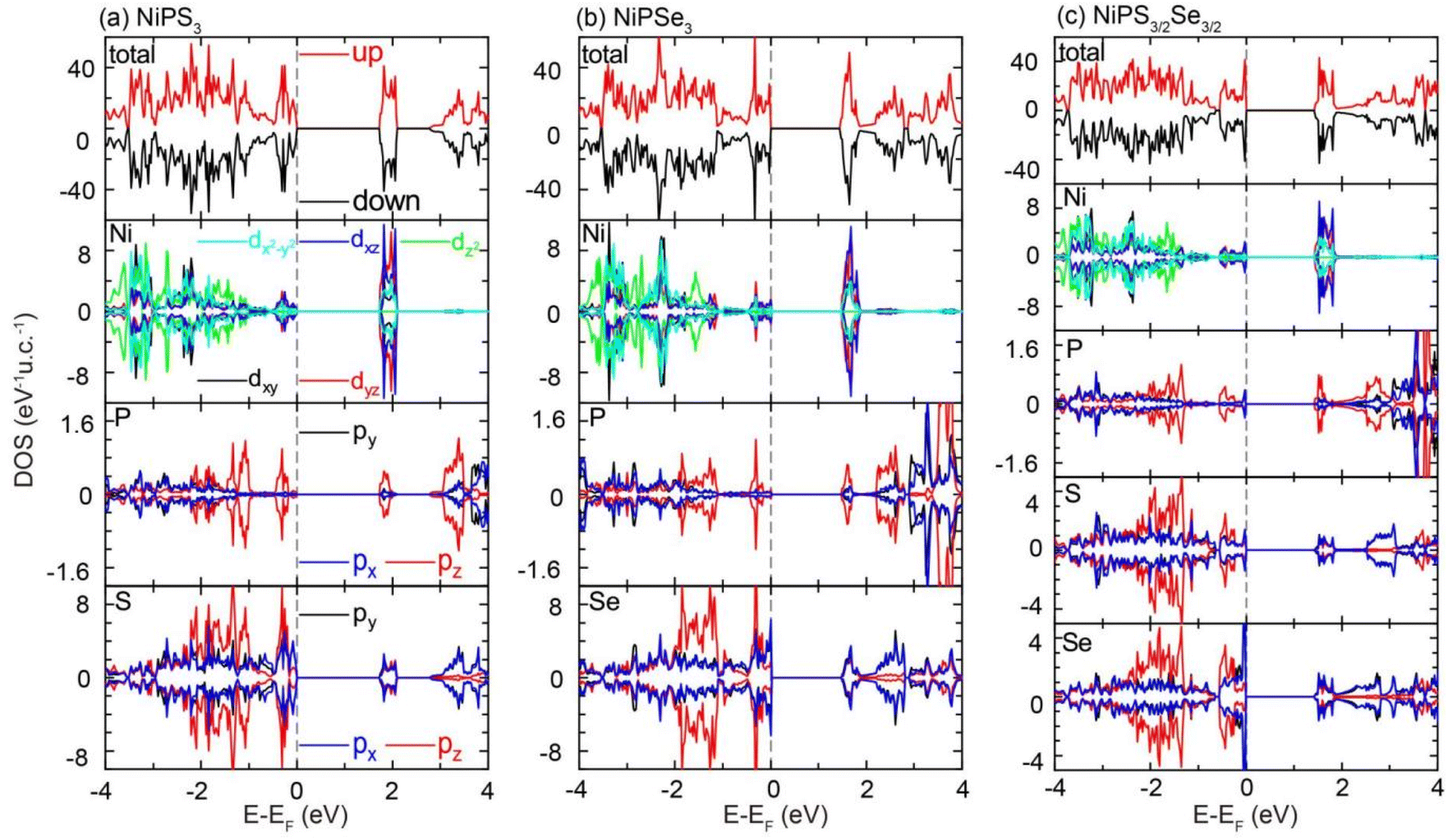 | ||
| Fig. 5 Total density of states (DOS) and orbital-projected DOS of 2D (a) NiPS3, (b) NiPSe3 and (c) NiPS3/2Se3/2. | ||
The electron numbers N were calculated by integrating the PDOS in the spin-up channel within the energy range from −0.50 eV to 0.0 eV by the formula of N = κ∫PDOSdE, where κ = 1/2 for pristine structures and κ = 1 for Janus phase, based on their respective molecular formulas. As listed in Table S1,† the electron numbers of the chalcogen elements in their p orbitals were calculated to be NS = 1.82 e for NiPSe3 and NSe = 1.96 e for NiPSe3, while NS = 0.94 e and NSe = 2.33 e for NiPS3/2Se3/2. These results clearly indicated that the Se element exhibited more influence on the electronic structures and magnetic properties than the S element for NiPS3/2Se3/2. As a consequence, the bandgap, MAE value and magnetic exchange parameters of Janus NiPS3/2Se3/2 were much closer to that of NiPSe3 than that of NiPS3. Here, Ni d electrons contributed more to the four undermost CBs than to the four uppermost VBs near the Fermi level. These contributions were primarily composed of the dxz and dyz states, with some contributions from the dxy and dx2−y2 orbitals. This feature deviated from that of some other AFM TMPX3, such as CrPSe3 and MnPS3, where d electrons contributed more to the uppermost VBs than to the undermost CBs.10,12 Throughout the energy range, P pz orbitals strongly hybridized with those of S/Se atoms, forming the [P2X6]4− octahedrons that provided excellent mechanical stability for each monolayer. Notably, the Ni d orbitals exhibited pronounced hybridization with the chalcogen px and py orbitals, facilitating an indirect p–d exchange interaction for Ni ions.
As illustrated in Fig. S1 and S2,† both the spin charge density maps and charge distributions of the Ni hexagonal slide could not provide enough information for the bonding behavior between Ni ions. Here, the electronic structures were further evaluated by extracting the chemical bonding data from COHP diagrams for NiPX3 and NiPS3/2Se3/2 monolayers. The negative diagrams of NN Ni–Ni couplings are plotted in Fig. 6(a)–(c), respectively. In these –COHP diagrams, the bonding and antibonding states were denoted by positive and negative values, respectively. It was evident that there were four negative peak-curves for –COHP below the Fermi level, where the plus/minus signs of –COHP peaks alternated from −6.0 eV to Fermi energy, which was set to 0.0 eV. In particular, the first main peak, situated just under Fermi level, exhibited negative values, which played a vital role in the zAFM configuration.
 | ||
| Fig. 6 –COHP distributions between NN Ni ions in 2D (a) NiPS3, (b) NiPSe3 and (c) NiPS3/2Se3/2. | ||
The coexistence of FM and AFM couplings between NN Ni ions was discussed by considering both the crystal field effect and electronic structure to clarify the mechanism of zAFM ordering. As shown in Fig. 7(a), each Ni atom was surrounded by six S/Se atoms, forming an octahedral structure with D3d symmetry.51,59 Owing to crystal field effect, Ni 3d orbitals could be divided into two parts: one group was named as t2g of the dxy, dx2−y2 and dz2 orbitals and the other one was denoted as eg of dxz and dyz orbitals. According to the orbital-projected DOS in Fig. 5, the energy of the t2g state was lower than that of the eg state in VBs; thus, the first negative –COHP peak under 0.0 eV was composed of eg states. Since Ni 3d electrons were in a configuration of 3d8 4s2, the t2g orbitals were fully occupied at the lower energy level, yielding no net magnetic moment. In contrast, the half-filled dxz/dyz orbitals had two electrons in the higher energy level with the same-direction spin alignment, resulting in a net magnetic moment with a calculated value about 1.40μB for each Ni ion. As illustrated in Fig. 7(b), the AFM exchange interactions could be attributed to the direct hopping between the half-filled eg orbitals for NN Ni ions, forming some bonding states. Comparatively, in Fig. 7(c), when NN Ni ions formed an FM arrangement, the FM exchange interactions could be realized by some antibonding states according to Hund's rule. As a consequence, the alternation of antibonding and bonding states led to the coexistence of AFM and FM couplings between NN Ni ions in NiPX3 and NiPS3/2Se3/2 monolayers.
 | ||
| Fig. 7 Schematic of (a) octahedral crystal field and 3d electron fillings and (b) AFM, and (c) FM exchange interactions between NN Ni ions. | ||
As discussed above, the first negative –COHP peak could be considered as a result of the FM coupling between eg orbitals in the antibonding states, resulting in positive J1 values. In other words, the FM indirect interactions between the NN Ni ions dominated the competition against the AFM direction exchange interactions, as illustrated in Fig. 1. However, the AFM ground states of NiPX3 and NiPS3/2Se3/2 were predominantly determined by the 3NN superexchange interactions mediated via p–d hybridization. Evidently, the absolute value J3 significantly exceeded J1, whereas the value of J2 was negligible. This huge difference between J2 and J3 originated from their distinct superexchange pathways. As shown in Fig. 1, the 2NN interactions were mediated by two S/Se atoms residing in different sublayers (one in the upper and the other in the lower), while the 3NN interactions were mediated by two S/Se atoms within the same sublayer. Here, the magnetic mechanism of Janus NiPS3/2Se3/2 was consistent with that of the pristine NiPX3 system; thus, the magnetic properties, including MAE, exchange parameters and TN values of NiPS3/2Se3/2 were similar to those of NiPX3 in the zAFM state. This stable magnetic feature was consistent with our previous findings on the MnPX3 system in the nAFM state.10
4. Conclusion
In summary, the electronic structures and magnetic properties of 2D pristine NiPX3 and Janus phase NiPS3/2Se3/2 were comprehensively investigated using the first-principles calculations. Despite the on-site Coulomb repulsion with a series of Ueff values, both pristine and Janus NiPX3 systems remained in a zAFM ground state and were characterized as indirect band gap semiconductors. The bandgaps of NiPS3 and NiPSe3 were 1.71 eV and 1.44 eV, respectively, while the value of NiPS3/2Se3/2 was 1.42 eV. Three 2D monolayers showed excellent structural stability as determined using the elastic coefficients satisfying the Born criterion, phonon spectra with no negative frequency and a planar structure after AIMD relaxation. Calculated MAE values showed that the magnetic easy-magnetization axis was in the z-axis direction for NiPSe3 and NiPS3/2Se3/2, while it was in the xy-plane for NiPS3. The magnetic exchange parameters for NiPS3 was J1 = 3.14 meV, J2 = 0.42 meV and J3 = −15.17 meV, for NiPSe3 was J1 = 4.33 meV, J2 = −0.03 meV and J3 = −18.68 meV and for NiPS3/2Se3/2 was J1 = 4.00 meV, J2 = −0.03 meV, and J3 = −17.30 meV. Néel temperatures predicted using Monte Carlo simulations were 160 K for NiPS3, 189 K for NiPSe3, and 180 K for NiPS3/2Se3/2. The magnetic properties of Janus NiPS3/2Se3/2 were more similar to those of pristine NiPSe3 because the Se p orbitals contributed more to the uppermost valence bands than the S p states for NiPS3/2Se3/2. The AFM ground state was determined by evaluating the large superexchange interactions mediated by p–d hybridization for 2D NiPX3 in both the pristine structure and Janus phase. Furthermore, the coexistence of antibonding and bonding states under the Fermi level led to FM couplings and AFM couplings between NN Ni ions, which could be clearly clarified by the crystal field effect and crystal orbital Hamilton populations.Data availability
The data supporting this article have been included as part of the ESI.†Conflicts of interest
There are no conflicts to declare.Acknowledgements
This work was supported by the programs of Innovation Team in Colleges for Science and Technology of Education Department of Hubei Province (No. T2021012), Doctoral Scientific Research Foundation of HUAT (BK202483, BK202208 and BK202302), Hubei key Laboratory of Energy Storage and Power Battery (No. QCCLSZK2021A06), Open Foundation Project of Hubei Key Laboratory of Optical Information and Pattern Recognition (No. 202403), WIT and College Students' Innovation and Entrepreneurship Training Program (DC2023074 and DC2024087).References
- X. Wang, K. Du, Y. Y. F. Liu, P. Hu, J. Zhang, Q. Zhang, M. H. S. Owen, X. Lu, C. K. Gan and P. Sengupta, et al., 2D Mater., 2016, 3, 1 CAS.
- J.-U. Lee, S. Lee, J. H. Ryoo, S. Kang, T. Y. Kim, P. Kim, C.-H. Park, J.-G. Park and H. Cheong, Nano Lett., 2016, 16, 7433 CrossRef CAS.
- P. Li, X. Li, J. Feng, J. Ni, Z.-X. Guo and H. Xiang, Phys. Rev. B, 2024, 109, 214418 CrossRef CAS.
- R. Brec, Solid State Ionics, 1986, 22, 3 CrossRef CAS.
- A. Wiedenmann, J. Rossat-Mignod, A. Louisy, R. Brec and J. Rouxel, Solid State Commun., 1981, 40, 1067 CrossRef CAS.
- W. Klingen, R. Ott and H. Hahn, Z. Anorg. Allg. Chem., 1973, 396, 271 CrossRef CAS.
- F. Wang, T. A. Shifa, P. Yu, P. He, Y. Liu, F. Wang, Z. Wang, X. Zhan, X. Lou and F. Xia, et al., Adv. Funct. Mater., 2018, 28, 1802151 CrossRef.
- K.-z. Du, X.-z. Wang, Y. Liu, P. Hu, M. I. B. Utama, C. K. Gan, Q. Xiong and C. Kloc, ACS Nano, 2016, 10, 1738 CrossRef CAS.
- B. L. Chittari, Y. Park, D. Lee, M. Han, A. H. MacDonald, E. Hwang and J. Jung, Phys. Rev. B, 2016, 94, 184428 CrossRef.
- J.-T. Yang, C.-J. Xu, H.-J. Wang, Q. Min, S.-J. Luo, Y.-C. Xiong, W. Ren and C. Jing, J. Phys.: Condens. Matter., 2023, 35, 395501 CrossRef CAS.
- Y. Sugita, T. Miyake and Y. Motome, Phys. Rev. B, 2018, 97, 035125 CrossRef CAS.
- J. Yang, Y. Zhou, Y. Dedkov and E. Voloshina, Adv. Theory Simul., 2020, 2000228 CrossRef CAS.
- Y. Jin, M. Yan, T. Kremer, E. Voloshina and Y. Dedkov, Sci. Rep., 2022, 12, 735 CrossRef CAS.
- S. Y. Kim, T. Y. Kim, L. J. Sandilands, S. Sinn, M.-C. Lee, J. Son, S. Lee, K.-Y. Choi, W. Kim and B.-G. Park, et al., Phys. Rev. Lett., 2018, 120, 136402 CrossRef CAS.
- S. Y. Lim, K. Kim, S. Lee, J.-G. Park and H. Cheong, Curr. Appl. Phys., 2021, 21(1) CrossRef.
- A. Wildes, B. Fåk, U. Hansen, M. Enderle, J. Stewart, L. Testa, H. Rønnow, C. Kim and J.-G. Park, Phys. Rev. B, 2023, 107, 054438 CrossRef CAS.
- Y. Wang, Z. Zhou, T. Wen, Y. Zhou, N. Li, F. Han, Y. Xiao, P. Chow, J. Sun and M. Pravica, et al., J. Am. Chem. Soc., 2016, 138, 15751 CrossRef CAS.
- Y. Wang, J. Ying, Z. Zhou, J. Sun, T. Wen, Y. Zhou, N. Li, Q. Zhang, F. Han and Y. Xiao, et al., Nat. Commun., 2018, 9, 1914 CrossRef.
- H. Sun, L. Qiu, Y. Han, E. Yi, J. Li, M. Huo, C. Huang, H. Liu, M. Li and W. Wang, et al., Mater. Today Phys., 2023, 36, 101188 CrossRef CAS.
- Q. Zhang, K. Hwangbo, C. Wang, Q. Jiang, J.-H. Chu, H. Wen, D. Xiao and X. Xu, Nano Lett., 2021, 21, 6938 CrossRef CAS.
- Z. Ni, A. Haglund, H. Wang, B. Xu, C. Bernhard, D. Mandrus, X. Qian, E. Mele, C. Kane and L. Wu, Nat. Nanotechnol., 2021, 16, 782 CrossRef CAS.
- A. Ghosh, M. Palit, S. Maity, V. Dwij, S. Rana and S. Datta, Phys. Rev. B, 2021, 103, 064431 CrossRef CAS.
- E. Ergęcen, B. Ilyas, D. Mao, H. C. Po, M. B. Yilmaz, J. Kim, J.-G. Park, T. Senthil and N. Gedik, Nat. Commun., 2022, 13, 98 CrossRef.
- F. Dirnberger, R. Bushati, B. Datta, A. Kumar, A. H. MacDonald, E. Baldini and V. M. Menon, Nat. Nanotechnol., 2022, 17, 1060 CrossRef CAS.
- P. Li, X. Li, J. Feng, J. Ni, Z.-X. Guo and H. Xiang, Phys. Rev. B, 2024, 109, 214418 CrossRef CAS.
- M. Amirabbasi and P. Kratzer, Phys. Rev. B, 2023, 107, 024401 CrossRef CAS.
- R. Basnet, K. M. Kotur, M. Rybak, C. Stephenson, S. Bishop, C. Autieri, M. Birowska and J. Hu, Phys. Rev. Res., 2022, 4, 023256 CrossRef CAS.
- J. Hafner, J. Comput. Chem., 2008, 29, 2044 CrossRef CAS.
- G. Kresse and J. Hafner, Phys. Rev. B: Condens. Matter Mater. Phys., 1993, 47, 558 CrossRef CAS.
- L. Matthes, O. Pulci and F. Bechstedt, J. Phys.: Condens. Matter, 2013, 25, 395305 CrossRef.
- B. Himmetoglu, A. Floris, S. De Gironcoli and M. Cococcioni, Int. J. Quant. Chem., 2014, 114, 14 CrossRef CAS.
- S. Maintz, V. L. Deringer, A. L. Tchougréeff, and R. Dronskowski, Lobster: A Tool to Extract Chemical Bonding from Plane-Wave based DFT, 2016 Search PubMed.
- H. J. Monkhorst and J. D. Pack, Phys. Rev. B: Condens. Matter Mater. Phys., 1976, 13, 5188 CrossRef.
- R. Dronskowski and P. E. Bloechl, J. Phys. Chem., 1993, 97, 8617 CrossRef CAS.
- A. Togo and I. Tanaka, Scr. Mater., 2015, 108, 1 CrossRef CAS.
- G. J. Martyna, M. L. Klein and M. Tuckerman, J. Chem. Phys., 1992, 97, 2635 CrossRef.
- C. Braga and K. P. Travis, J. Chem. Phys., 2005, 123, 134101 CrossRef.
- R. Blankenbecler, D. Scalapino and R. Sugar, Phys. Rev. D, 1981, 24, 2278 CrossRef CAS.
- H. Haario, E. Saksman and J. Tamminen, Bernoulli, 2001, 223–242 CrossRef.
- K. Momma and F. Izumi, J. Appl. Crystallogr., 2011, 44, 1272 CrossRef CAS.
- V. Wang, N. Xu, J.-C. Liu, G. Tang and W.-T. Geng, Comput. Phys. Commun., 2021, 267, 108033 CrossRef CAS.
- A. R. Wildes, V. Simonet, E. Ressouche, G. J. McIntyre, M. Avdeev, E. Suard, S. A. J. Kimber, D. Lançon, G. Pepe and B. Moubaraki, et al., Phys. Rev. B: Condens. Matter Mater. Phys., 2015, 92, 224408 CrossRef.
- G. Le Flem, R. Brec, G. Ouvard, A. Louisy and P. Segransan, J. Phys. Chem. Solids, 1982, 43, 455 CrossRef CAS.
- F. Knuth, C. Carbogno, V. Atalla, V. Blum and M. Scheffler, Comput. Phys. Commun., 2015, 190, 33 CrossRef CAS.
- E. Cadelano, P. L. Palla, S. Giordano and L. Colombo, Phys. Rev. B: Condens. Matter Mater. Phys., 2010, 82, 235414 CrossRef.
- R. C. Andrew, R. E. Mapasha, A. M. Ukpong and N. Chetty, Phys. Rev. B: Condens. Matter Mater. Phys., 2012, 85, 125428 CrossRef.
- A. Togo, J. Phys. Soc. Jpn., 2023, 92, 012001 CrossRef.
- P. Giannozzi, S. De Gironcoli, P. Pavone and S. Baroni, Phys. Rev. B, 1991, 43, 7231 CrossRef CAS.
- H. J. Xiang, E. J. Kan, S.-H. Wei, M.-H. Whangbo and X. G. Gong, Phys. Rev. B: Condens. Matter Mater. Phys., 2011, 84, 224429 CrossRef.
- S. Yan, Y. Du, X. Zhang, X. Wan and D. Wang, J. Phys.: Condens. Matter, 2023, 36, 065502 CrossRef.
- Y. Gu, Q. Zhang, C. Le, Y. Li, T. Xiang and J. Hu, Phys. Rev. B: Condens. Matter Mater. Phys., 2019, 100, 165405 CrossRef CAS.
- Y. Lee, C. Kim, S. Son, J. Cui, G. Park, K.-X. Zhang, S. Oh, H. Cheong, A. Kleibert and J.-G. Park, Nano Lett., 2024, 24, 6043 CrossRef CAS.
- R. Basnet, K. M. Kotur, M. Rybak, C. Stephenson, S. Bishop, C. Autieri, M. Birowska and J. Hu, Phys. Rev. Res., 2022, 4, 023256 CrossRef CAS.
- J.-T. Yang, C.-J. Xu, H.-J. Wang, Q. Min, S.-J. Luo, Y.-C. Xiong, W. Ren and C. Jing, J. Phys.: Condens. Matter, 2023, 35, 395501 CrossRef CAS.
- Q. H. Wang, A. Bedoya-Pinto, M. Blei and A. H. Dismukes, et al., ACS Nano, 2022, 16, 6960 CrossRef CAS.
- S. Toyoda, J. Kruppe, K. Yamakawa, J. Analytis and J. Orenstein, Phys. Rev. B, 2024, 109, 064408 CrossRef CAS.
- V. Popescu and A. Zunger, Phys. Rev. Lett., 2010, 104, 236403 CrossRef.
- P. Foot, J. Suradi and P. Lee, Mater. Res. Bull., 1980, 15, 189 CrossRef CAS.
- C. Autieri, G. Cuono, C. Noce, M. Rybak, K. M. Kotur, C. E. Agrapidis, K. Wohlfeld and M. Birowska, J. Phys. Chem. C, 2022, 126, 6791 CrossRef CAS.
Footnote |
| † Electronic supplementary information (ESI) available. See DOI: https://doi.org/10.1039/d5ra02861b |
| This journal is © The Royal Society of Chemistry 2025 |