
 Open Access Article
 This Open Access Article is licensed under a Creative Commons Attribution-Non Commercial 3.0 Unported Licence
DFT analysis of the physical properties of direct band gap semiconducting double perovskites A2BIrCl6 (A = Cs, Rb; B = Na, K) for solar cells and optoelectronic applications†
Md. Tarekuzzaman a,
Nazmul Shahadatha,
Mufrat Montasira,
O. Alsalmib,
M. H. Miacd,
Hmoud Al-Dmoure,
Md. Rasheduzzamana and
Md. Zahid Hasan*a
a,
Nazmul Shahadatha,
Mufrat Montasira,
O. Alsalmib,
M. H. Miacd,
Hmoud Al-Dmoure,
Md. Rasheduzzamana and
Md. Zahid Hasan*a
aMaterials Research and Simulation Lab, Department of Electrical and Electronic Engineering, International Islamic University Chittagong, Kumira, Chittagong, 4318, Bangladesh. E-mail: zahidhasan.02@gmail.com
bDepartment of Physics, College of Science, Umm Al-Qura University, Makkah 21955, Saudi Arabia
cDepartment of Textile Engineering, Northern University Bangladesh, Uttara, Dhaka, Bangladesh
dDepartment of Computer and Communication Engineering, International Islamic University Chittagong, Kumira, Chattogram-4318, Bangladesh
eDepartment of Physics, Faculty of Science, Mutah University, karak 61710, Jordan
First published on 28th April 2025
Abstract
Double perovskite-based optoelectronic devices are gaining attention due to their unique characteristics, including a simple and stable crystal structure. This study employs density functional theory (DFT) with the full-potential linearized augmented plane-wave (FP-LAPW) method to investigate the structural, electronic, optical, mechanical, and thermodynamic properties of A2BIrCl6 (A = Cs, Rb; B = Na, K) double perovskite halides. The primary aim is to assess their potential applicability in optoelectronic devices and renewable energy technologies. The cubic stability of the predicted compounds was confirmed through the Goldsmith tolerance factor, octahedral factor, and a new tolerance factor. Additionally, to confirm their thermodynamic stability, we assessed the formation energy, binding energy, and phonon dispersion curves. We used the TB-mBJ potential to accurately predict the optoelectronic properties. The calculations of the electronic band structure indicated that the examined double perovskites exhibit a direct band gap semiconducting nature, with the following band gap values: 1.927 eV for Cs2NaIrCl6 1.991 eV for Cs2KIrCl6, 2.025 eV for Rb2NaIrCl6, and 2.102 eV for Rb2KIrCl6. The A2BIrCl6 (A = Cs, Rb; B = Na, K) compounds demonstrate impressive optical properties, including low reflectivity and high light absorption coefficients (104 cm−1) in the visible spectrum. Their spectral response extends from the visible to the UV range, making them ideal candidates for applications in solar cells and optoelectronic devices. The mechanical stability of the titled compounds was confirmed through the Born–Huang stability conditions based on their stiffness constants. The brittle nature of all the examined perovskites is confirmed by Pugh's ratio, Cauchy pressure, and Poisson's ratio. Finally, the Helmholtz free energy (F), internal energy (E), entropy (S), and specific heat capacity (Cv) are calculated based on the phonon density of states.
1. Introduction
The global energy crisis is intensifying daily because of increasing demand. For many years, burning fossil fuels like coal, oil (petroleum), and natural gas has released carbon dioxide and other pollutants into the atmosphere, which has led to environmental issues including air pollution and climate change. As a result, governments have had to look for alternative energy sources to replace coal, gasoline, oil, and other fossil fuels, which has been highlighted by the quick growth of technical developments and the escalating environmental concerns. Renewable energy can be a good option to lessen these effects on the environment. Renewable energy can be produced by decomposing organic waste, allowing for the capture and use of emitted gases for power production via generators. Moreover, solar and thermal energy conversion materials offer a sustainable alternative to environmentally harmful materials, particularly carbon-based fuels.1,2 The two primary sources of renewable energy are solar energy and waste heat, which can be applicable in photovoltaic and thermoelectric procedures. Renewable energy sources like photovoltaics, thermoelectrics, and devices are great for the economy and technology since they are credible, affordable, and constantly functional. The capacity to execute thermal and photoelectric functions is contingent upon the selection of materials. The industry places great priority on the development of new solar cell technologies and materials with high inbuilt stability, high efficiency, and lower production costs. For the aforementioned procedures, perovskite halide materials are very promising. In the area of materials research, perovskite halides represent a fundamental change, as they provide a versatile substrate for a diverse array of usages, with solar power at the vanguard.Halide perovskite materials have demonstrated remarkable capabilities as semiconductors, showcasing outstanding performance in applications like solar cells and lasers.3,4 Hybrid perovskites, both organic and inorganic, have emerged as a prominent category of optoelectronic materials, showcasing record solar efficiencies alongside encouraging demonstrations of LEDs and transistors.5–8 Innovative classes of perovskites, including double or complex halide perovskites have received significant attention for their exceptional efficiency and eco-friendliness.9–11 Double perovskites are typically represented by the formula A2BB′X6, in which the A and B sites suggest the presence of a variety of elements.12 Halide double perovskite photovoltaic cells have been stabilized through partial or complete substitution of the A-site/B-site cation and X-site anion.13 The characteristics of halide double perovskites make them valuable in several fields, including photo-catalysis, storage gadgets, X-ray sensors, indoor photovoltaics, LEDs, and plenty more.14–17 Furthermore, a single perovskite is limited to accommodating only the 2+ cationic configuration in B-sites, while a double perovskite is capable of handling an even wider range, ranging from 1 to 4+.18 Because of this, the double perovskite provides better functionality, tunability, stability, lower defect density, band gap engineering flexibility, and continual usage advantages.
As a consequence, extensive investigations are underway to assess the viability of these materials for power generating applications. Perovskite materials, CH3NH3PbI3, are composed of a hybrid organic–inorganic mixture and includes lead. The performance of these compounds in optoelectronic devices and solar cells has shown significant improvements, leading to enhanced efficiency.19,20 The meticulous analysis carried out has led to a remarkable enhancement in efficiency, showing a substantial rise from 3.8% in 2009 to 25.2% in 2020. On top of that, improvements in this area have also raised efficiency which is now 29.1%.21 They exhibit a direct energy band gap, a noticeable absorption in the visible spectrum, and stable electron–hole masses.22,23 A combination of toxicity, environmental pollution, and health hazards makes Pb-based compounds less reliable. The radioactive instability of lead and its negative impacts on the environment make the substitution with other elements imperative. Consequently, there is an increasing need for nontoxic lead-free PSCs, prompting the development of various lead-free perovskite materials. In the pursuit of alternatives to lead-based perovskites, Pb2+ is being substituted with a range of nontoxic components, such as bivalent Sn2+ and Ge2+.24
Nonetheless, replacing lead with Ge or Sn, which belong to the same group, is viewed as more advantageous; yet, this change results in a 10% decrease in efficiency.25,26 A further layer of difficulty has been added due to the fact that Sn and Ge both exhibit variable valence electrons (+4, +2), which impacts their long-term endurance.27 Additionally, Pb2+ has also been substituted with heterovalent M3+, like Bi3+, which is non-toxic, isoelectronic with Pb2+, and exhibits stability in semiconducting halides.28 Because their inherent trap densities and defect density are smaller, bismuth-based PSCs have longer charge carrier diffusion durations.19 However, adding a highly charged Bi3+ ion to the lead-based perovskite also resulted in worse optoelectronic properties.21,22 In addition, lead can be substituted with a complex mixture of monovalent and trivalent cations, whose structural formula is A2B′B′′Z6. Here, “A” denotes a large cation (Rb + or Cs+), B′ and B′′ denote trivalent or monovalent cations, and “Z” denotes oxygen or halogens. Recently, the halide perovskite Cs2InAgCl6, which is silver based, has been successfully synthesized and characterized.29 Nevertheless, a large number of these perovskite materials show a deficient optical profile or a wide bandgap, which suggests they are only useful for limited functions in the industry of solar energy.
Additionally, scientific investigation has shown that the perovskite compound referred to as Cs2AgInCl6 features a direct bandgap and demonstrates significant stability. Regardless, adding more halides appears to make the perovskite structure less stable. The observed instability in perovskite materials could be associated with the presence of trapped states and structural defects, as indicated by the analysis of charge carrier relaxation and photoluminescence (PL).30,31 In addition, the perovskite materials Rb2AgInCl6 and Cs2AgInCl6 have been shown to have substantial direct band gaps, which is very important when looking for compounds with outstanding solar capabilities.32 Reports have been highlighted that the wide band gap In-based perovskites X2CuInCl6 (where X= Rb, K, or Cs) and Rb2InSbX6 (where X = Cl, Br) have remarkable optical absorption and thermoelectric characteristics.33,34 Recent reports indicate that the wide band gap Na-based and K-based perovskite Rb2Na/KInX6 (where X = Br and I) are promising candidates for thermoelectric and solar energy uses.35 A similar stable molecule, Cs2NaTIBr6, based on sodium, has been the subject of a recent theoretical investigation. With a straight bandgap of 1.82 eV, it now has a great chance of being used in photovoltaic applications.36 Similarly, another study reported that Rb2NaTlZ6 (Z = Cl, Br, and I) have a direct band gap values of 3.4, 2.6, and 2.1 eV and he light absorption coefficients exhibited absorption in the visible and ultraviolet regions of the spectrum. Within these specific energy regions, there was very little loss of optical energy which suggests that these materials will be a promising candidate for optoelectronic and photovoltaic devices.37 Furthermore, Cs2InAsF6, Cs = RbIrF6, and Cs2NaRhF6 exhibit a direct band gap and values of 2.76 eV, 3.78 eV and 3.6 eV, respectively and they exhibit absorption in the ultraviolet (UV) region, indicating that they might be used as solar energy devices, laser and UV-shield components.38
The growing demand for optoelectronic devices underscores the importance of exploring and discovering additional members of the double perovskite family, despite the considerable research that has recently been conducted on various Cs and Rb based double perovskites. Here in our investigation, we also examined another group of double perovskites, A2BIrCl6 (A = Cs, Rb; B = Na, K). Therefore, this study has examined the structural stability, optoelectronic characteristics, and thermoelectric characteristics of the A2BIrCl6 (A = Cs, Rb; B = Na, K) double perovskites. We believe that our research will provide crucial direction for forecasting lead-free DP materials that might be used in next solar cells and thermoelectric devices. The thermo-mechanical properties of the materials under study were also covered in this article as a standard evaluation.
2. Methodology
In this study, we utilized first-principles computations to explore the structural, dynamical, electronic, optical, mechanical, and thermophysical properties of the double perovskite A2BIrCl6 (A = Cs, Rb; B = Na, K). Through the density functional theory (DFT) approach,39,40 the analysis was conducted using the Wien2k software, which is based on the FP-LAPW (Full-Potential Linearized Augmented Plane Wave) method and employs electronic wave functions.41 In this process, the Generalized Gradient Approximation (GGA) with the Perdew–Burke–Ernzerhof (PBE)42 approach is first employed to compute the ground state variables. Structural optimization is subsequently performed using the FP-LAPW method, guided by the third-order Birch–Murnaghan equation of state.43 The plane wave cutoff parameter, denoted as RMT × kmax was selected to be 8.0. Here, RMT refers to the radius of the smallest atomic muffin-tin sphere, while kmax is the maximum wave vector in the plane wave basis. Within the muffin tin sphere, a maximum partial wave component of lmax = 10 was defined. The radii of the atomic muffin-tin spheres were set individually as follows: RMT(Cs) = 2.50 a.u., RMT(K) = 2.13 a.u., RMT(Ir) = 2.18 a.u., and RMT(X) = 1.88 a.u. To precisely represent the potential and charge density, we utilized a Fourier series incorporating wave vectors up to Gmax = 14 (Ry1/2). To ensure computational precision, a dense k-point mesh consisting of 1000 (10 × 10 × 10) points was utilized within the first Brillouin zone (BZ). During SCF calculations, the criteria for energy convergence (ec) and charge convergence (cc) are defined as 10−5 Ry and 0.001e, respectively. The TB-mBJ (Trans Blaha modified Becke–Johnson)44 methodology was applied to assess optoelectronic characteristics, balancing precision and computational efficiency for inorganic compounds. We used the same k-mesh of 1000 points (10 × 10 × 10) for both the structure optimizations and the Trans Blaha-modified Becke–Johnson methodology. VESTA software was used to visualize the crystal structure.45 Additionally, using the Cambridge Serial Total Energy Package (CASTEP) code,46 the materials phonon dynamic stability was verified. To calculate phonons, a 1 × 1 × 1 supercell model of the unit cell structure was used. To assess the lattice dynamics, including phonon dispersion and thermodynamic properties, we utilized the supercell method with finite displacement. A cut-off energy of 500 eV is set for the plane-wave basis set. The convergence criteria are defined as 5 × 10⁻⁶ eV per atom for total energy, 5 × 10⁻⁴ Å for maximum displacement, 0.01 eV Å−1 for maximum force, and 0.02 GPa for maximum stress. To ensure accurate sampling of the reciprocal space, the Brillouin zone is integrated using a 2 × 2 × 2 k-point grid, following the Monkhorst–Pack scheme.3. Result and discussion
3.1 Structural properties and stability
Structural property analysis is fundamental for assessing various material characteristics, including the bandgap of semiconductors.47 In addition, the structural characteristics offer a clear understanding of the basic atomic configuration and the volume of the unit cell. The chemical formula A2BIrCl6 (where A represents Cs or Rb, and B represents Na or K) is composed of four distinct elements (A, B, Ir, and Cl) in a ratio of 2![[thin space (1/6-em)]](https://www.rsc.org/images/entities/char_2009.gif) :1:1:6. Double perovskites possess unique structural features and stability due to the combination of a large A-site cation and two distinct B-site cations. The typical crystal configuration of inorganic double halide perovskites A2BIrCl6 (A = Cs, Rb; B = Na, K) is depicted in Fig. 1. The double halide perovskites A2BIrCl6 (A = Cs, Rb; B = Na, K) crystallize in a cubic double-perovskite structure with an Fm
:1:1:6. Double perovskites possess unique structural features and stability due to the combination of a large A-site cation and two distinct B-site cations. The typical crystal configuration of inorganic double halide perovskites A2BIrCl6 (A = Cs, Rb; B = Na, K) is depicted in Fig. 1. The double halide perovskites A2BIrCl6 (A = Cs, Rb; B = Na, K) crystallize in a cubic double-perovskite structure with an Fm![[3 with combining macron]](https://www.rsc.org/images/entities/char_0033_0304.gif) m space group. The unit cell of A2BIrCl6 (where A = Cs, Rb; B = Na, K) contains a total of 10 atoms, including 2 atoms of A, 1 atom of B, 1 atom of Ir, and 6 atoms of Cl. In the unit cell, Cs/Rb atoms are positioned at 4a (0, 0, 0), Na/K are at 4b (0.5, 0, 0), Ir occupies 8c (0.25, 0.25, 0.75), and Cl is located at 24e (0.2513, 0, 0). The lattice parameters for Cs2NaIrCl6, Cs2KIrCl6, Rb2NaIrCl6, and Rb2KIrCl6 have been determined as 10.146 Å, 10.461 Å, 10.022 Å, and 10.359 Å, respectively. The estimated lattice parameter for the double perovskite (DP) A2BIrCl6 (A = Cs, Rb; B = Na, K) are tabulated in Table 1.
m space group. The unit cell of A2BIrCl6 (where A = Cs, Rb; B = Na, K) contains a total of 10 atoms, including 2 atoms of A, 1 atom of B, 1 atom of Ir, and 6 atoms of Cl. In the unit cell, Cs/Rb atoms are positioned at 4a (0, 0, 0), Na/K are at 4b (0.5, 0, 0), Ir occupies 8c (0.25, 0.25, 0.75), and Cl is located at 24e (0.2513, 0, 0). The lattice parameters for Cs2NaIrCl6, Cs2KIrCl6, Rb2NaIrCl6, and Rb2KIrCl6 have been determined as 10.146 Å, 10.461 Å, 10.022 Å, and 10.359 Å, respectively. The estimated lattice parameter for the double perovskite (DP) A2BIrCl6 (A = Cs, Rb; B = Na, K) are tabulated in Table 1.
 | ||
| Fig. 1 Conventional crystal structures of A2BIrCl6 (A = Cs, Rb; B = Na, K). | ||
 , total energy Etot (Ry), formation energy Ef (eV per atom), and binding energy EB (eV per atom) for double perovskite (DP) A2BIrCl6 (A = Cs, Rb; B = Na, K)
| DP | a0 (Å) | B0 (GPa) |
|
Etot (Ry) | Ef (eV per atom) | Eb (eV per atom) | References |
|---|---|---|---|---|---|---|---|
| Cs2NaIrCl6 | 10.146 | 38.20 | 5.00 | −72741.20 |
−2.37 | −4.39 | This |
| Cs2KIrCl6 | 10.461 | 33.77 | 2.38 | −73620.50 |
−2.40 | −4.37 | This |
| Rb2NaIrCl6 | 10.022 | 39.83 | 4.93 | −53505.98 |
−2.33 | −4.38 | This |
| Rb2KIrCl6 | 10.359 | 33.12 | 2.80 | −54385.27 |
−2.34 | −4.34 | This |

Additionally, the stability of double halide perovskites A2BIrCl6 (A = Cs, Rb; B = Na, K) can be evaluated through their formation energy and binding energy, derived from the given formulas.48
 | (1) |
| Eb=EA2BIrCl6−nA×μA−nB×μb−nIr×μIr−nCl×μCl | (2) |
 | ||
| Fig. 2 Birch–Murnaghan total energy vs. volume fitting curve for the A2BIrCl6 (A = Cs, Rb; B = Na, K). | ||
To evaluate the stability of a double perovskite material, parameters such as the tolerance factor (τ1), the physically derived new tolerance factor (τ2), and the octahedral factor (μ) are used. Their values are determined from the formulas shown below:49–51
 | (3) |
 | (4) |
 | (5) |
According to the eqn (3)–(5), RA (Cs, Rb), RB (Na, K), RIr, and RCl indicate the ionic radii of A (A = Cs, Rb), B (Na, K), Ir, and Cl, while nA denotes the oxidation state of A (Cs, Rb). For a compound to exhibit cubic stability, its tolerance factor (τ1), should range from 0.813 to 1.107,49 while the octahedral factor (μ) must fall within 0.41 to 0.89.51 The newly derived tolerance factor in our research demonstrates greater precision in forecasting structural stability than other approaches. Cubic stability in perovskites is expected when (τ2), remains under 4.18.50 We evaluated these parameters using Shannon's ionic radii. Table 2 illustrates that every compound analyzed maintains cubic structural stability.
| DP | Ionic radius of cations (Å) | Ionic radius of anion (Å) | Tolerance factor (τ1) | Octahedral factor (μ) | New tolerance factor (τ2) | |
|---|---|---|---|---|---|---|
| Cs2NaIrCl6 | rCs |  |
rCl | 0.98 | 0.47 | 3.54 |
| 1.88 | 0.85 | 1.81 | ||||
| Cs2KIrCl6 | rCs |  |
rCl | 0.92 | 0.57 | 3.80 |
| 1.88 | 1.03 | 1.81 | ||||
| Rb2NaIrCl6 | rRb |  |
rCl | 0.94 | 0.47 | 3.99 |
| 1.72 | 0.85 | 1.81 | ||||
| Rb2KIrCl6 | rRb |  |
rCl | 0.88 | 0.57 | 3.97 |
| 1.72 | 1.03 | 1.81 | ||||
Dynamic stability is crucial for ensuring durability and reliable performance of structures and materials under changing or fluctuating forces. Material stability is commonly analyzed through its phonon dispersion curve and phonon density of states (PHDOS). Phonons are crucial for understanding the dynamic behavior and thermal characteristics, which are key areas in materials science.52 The dynamic stability of the A2BIrCl6 (A = Cs, Rb; B = Na, K) compound was evaluated by calculating the PDC and PHDOS at high symmetry K points (W-L-Γ-X-W-K) in the BZ, as shown in Fig. 3(a–d). The absence of imaginary frequencies across the Brillouin zone (BZ) signifies the dynamic stability of crystalline materials. In opposition, the presence of an imaginary component denotes dynamic instability. The absence of negative frequencies in the phonon dispersion curve (PDC) of A2BIrCl6 (A = Cs, Rb; B = Na, K) suggests its dynamic stability. In a compound with N atoms, the primitive cell contains 3N (3 × 10) vibrational modes. The A2BIrCl6 (A = Cs, Rb; B = Na, K) compound, with 10 atoms, exhibits 30 vibrational modes in total, including 27 optical modes and 3 acoustic modes. As illustrated in Fig. 3, the acoustic modes at the Γ-point are observed to be zero. For a better understanding of the compound's properties, its phonon DOS (PHDOS) is displayed next to the dispersion curve. The figure demonstrates that fluctuations in the PDC are depicted as smaller peaks, whereas flat dispersion in the PDC corresponds to prominent peaks in the PHDOS. The PHDOS analysis reveals that the interaction between Cs/Rb and Cl atoms predominantly influences the lower-frequency phonon modes, while the Ir–Cl interaction produces the high-frequency phonon modes in all figures. Furthermore, the Na and K atoms significantly contribute to the middle-frequency phonon modes.
 | ||
| Fig. 3 Phonon dispersion curve along with phonon DOS of A2BIrCl6 (A = Cs, Rb; B = Na, K) compounds. | ||
3.2 Electronic properties
To deepen our understanding of how the physical attributes of double perovskites (DPs) adapt with structural variations, it is essential to analyze their electronic properties, particularly their band structures and partial density of states (PDOS). The calculated electronic band structures for A2BIrCl6 (A = Cs, Rb; B = Na, K) compounds, determined using GGA-PBE and the more advanced TB-mBJ functionals, are summarized in Table 3 and illustrated in Fig. 4 and 5. The Fermi level (EF) is indicated by a horizontal green dashed line positioned at 0 eV for reference. Our computational findings reveal that the conduction band minimum (CBM) and valence band maximum (VBM) are both located at the X point in the Brillouin zone, irrespective of the functional used. This confirms that A2BIrCl6 (A = Cs, Rb; B = Na, K) compounds possess a direct bandgap, a highly desirable feature for semiconductors due to the superior efficiency of optical transitions it enables. Such a direct alignment is particularly advantageous for optoelectronic applications, including solar cells and light-emitting devices (LEDs), where high photon absorption and emission efficiencies are critical.| Compounds | Band gap (eV) | Band gap nature |
|
|
|||
|---|---|---|---|---|---|---|---|
| GGA + PBE | TB-mBJ | GGA + PBE | TB-mBJ | GGA + PBE | TB-mBJ | ||
| Cs2NaIrCl6 | 0.917 | 1.927 | Direct | 0.21me | 0.30me | 1.33me | 1.69me |
| Cs2KIrCl6 | 1.048 | 1.991 | Direct | 0.23me | 0.32me | 1.51me | 1.98me |
| Rb2NaIrCl6 | 0.971 | 2.025 | Direct | 0.20me | 0.29me | 1.10me | 1.41me |
| Rb2KIrCl6 | 1.121 | 2.102 | Direct | 0.23me | 0.32me | 1.24me | 1.63me |


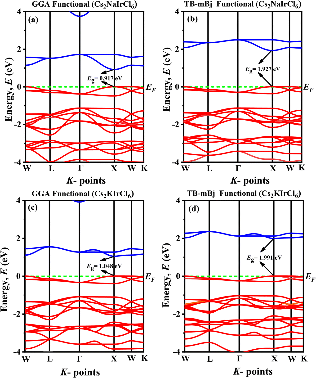 | ||
| Fig. 4 Band diagram of (a) Cs2NaIrCl6 (GGA), (b) Cs2NaIrCl6 (TB-mBj), (c) Cs2KIrCl6 (GGA), (d) Cs2KIrCl6 (TB-mBj). | ||
 | ||
| Fig. 5 Band diagram of (a) Rb2NaIrCl6 (GGA), (b) Rb2NaIrCl6 (TB-mBj), (c) Rb2KIrCl6 (GGA), (d) Rb2KIrCl6 (TB-mBj). | ||
The bandgap values for the studied compounds range from 0.917 eV to 1.121 eV (GGA + PBE) and 1.927 eV to 2.102 eV (TB-mBJ), as seen in Table 3. The broader bandgap range calculated using TB-mBJ, renowned for its accuracy in bandgap estimation, reflects a more reliable prediction of the electronic structure.44 These bandgaps indicate the semiconducting nature of the materials and their suitability for visible-to-near-infrared (NIR) optoelectronic applications. Moreover, the substitution of smaller cations (e.g., Rb instead of Cs or K instead of Na) systematically increases the bandgap. This trend suggests a shift in optical absorption towards shorter wavelengths and enhanced insulating properties. These findings highlight the critical role of cation substitutions and lattice distortions in fine-tuning the electronic properties of these materials.
To further elucidate the band structures, the partial density of states (PDOS) and total density of states (TDOS) of the double perovskite compounds A2BIrCl6 (A = Cs, Rb; B = Na, K) were analyzed, as depicted in Fig. 6. The vertical dashed line at 0 eV represents the Fermi energy (EF). A clear bandgap (Eg) is observed in the TDOS diagrams of all compounds, confirming their semiconducting nature. In the case of A2BIrCl6 (A = Cs, Rb; B = Na, K), the valence band is primarily derived from the Ir-5d and Cl-3p orbitals, while the conduction band is dominated by the Ir-5d orbitals with notable contributions from Cl-3p. The hybridization between Ir-5d and Cl-3p states plays a pivotal role in determining the electronic structure. Substitution of smaller cations (Rb instead of Cs or K instead of Na) enhances this hybridization, which increases the bandgap slightly and shifts the absorption toward shorter wavelengths. The negligible contributions of A-site and B-site cations to both the valence and conduction bands indicate that their role is primarily structural stabilization rather than active participation in electronic transitions. The Ir 5d orbitals are pivotal in defining the electronic structure, making Ir the principal determinant of the semiconducting and optoelectronic properties of these compounds.
 | ||
| Fig. 6 Total DOS and partial DOS of (a) Cs2NaIrCl6, (b) Cs2KIrCl6, (c) Rb2NaIrCl6, (d) Rb2KIrCl6. | ||
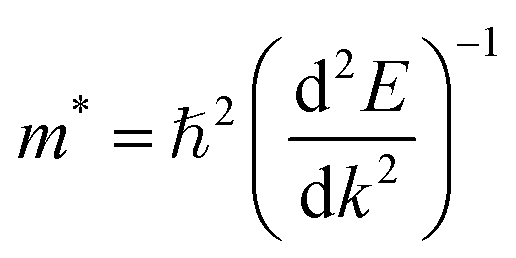
The effective mass (m*) is a key parameter that describes how electrons  and holes
  respond to external forces, such as electric fields, within a semiconductor. A smaller effective mass for electrons or holes indicates higher mobility, leading to enhanced charge transport, which is crucial for optoelectronic device performance. The effective mass (m*) of A2BIrCl6 (A = Cs, Rb; B = Na, K) is calculated by fitting the actual E–k curve around the conduction band minimum (CBM) and the valence band maximum (VBM) at the X-point. This calculation uses the equation:53
 | (6) |
 and holes
  in A2BIrCl6 (A = Cs, Rb; B = Na, K) vary among the four compounds, reflecting differences in their electronic structures. Electron effective masses
  are relatively low, ranging from 0.20–0.23m0 (GGA + PBE) to 0.29–0.32m0 (TB-mBJ), whereas hole effective masses
  are higher, spanning 1.10–1.51m0 (GGA + PBE) to 1.41–1.98m0 (TB-mBJ). Among these, Rb2NaIrCl6 exhibits the lowest
  and
and  , making it the most promising material for enhanced charge carrier mobility. Lower effective masses, as seen in Rb2NaIrCl6, enable higher carrier mobility, crucial for efficient charge transport in optoelectronic applications. In contrast, Cs2KIrCl6 has the highest
  , indicating reduced hole mobility, which may hinder its performance in applications requiring balanced charge transport, such as solar cells and light-emitting devices. The variations in effective mass stem from structural and orbital factors. Smaller cations like Rb (vs. Cs) and Na (vs. K) introduce lattice distortions, enhancing orbital overlap and reducing effective mass. Additionally, strong Ir 5d–Cl 3p hybridization broadens the bands, lowering effective mass. Compounds with higher effective masses experience weaker hybridization and narrower bands.
3.3 Nature of bonding
Charge density mapping offers a method to study electron density in materials, giving clues about their bonding and electronic structures. This method identifies areas of high and low electron density in the crystal structure, providing insights into the nature of bonding, whether ionic, covalent, or metallic. Charge density mapping for A2BIrCl6 (A = Cs, Rb; B = Na, K) provides key insights into the bonding interactions among the constituent atoms. As a part of the double perovskite family, A2BIrCl6 (A = Cs, Rb; B = Na, K) exhibits captivating characteristics due to its exceptional bonding and crystal framework. The cubic crystal structure of these materials, classified under space group Fmm, reflects the significant contributions of cations (Cs+/Rb+) and the lattice to their properties. In this configuration, the Cl ions are centrally located in the octahedra, while Na and K ions occupy the corners, sharing the octahedral spaces. The spaces between the Cs+/Rb+ ions create interstitial regions. This arrangement forms a network of octahedra connected at the corners, influencing the compound's electronic and bonding properties. Fig. 7 presents the charge density contour map for these compounds. The A ions (Cs/Rb) are more electronegative than B ions (Na, K), leading to ionic bonding with the nearby Cl ions. This leads to the formation of A–Cl bonds with a strong ionic character. The B (Na, K)–Ir–Cl octahedral structure is characterized by covalent bonding between the metal ions (B and Ir) and the halogen ions (Cl). The creation of polar covalent bonds within the octahedral structure is attributed to the difference in electronegativity between the metal ions and Cl ions, as seen in prior studies.54 The B–Ir bonding in the octahedral structure could also display metallic properties due to the overlap of their atomic orbitals. The distribution of charge density in materials is influenced by a combination of ionic, covalent, and metallic bonding interactions. The A ions generate a localized positive charge density, while the Cl ions create a localized negative charge due to their greater electronegativity. The unique bonding in A2BIrCl6 (A = Cs, Rb; B = Na, K), driven by covalent, ionic, and metallic interactions, is key to its excellent photovoltaic performance.
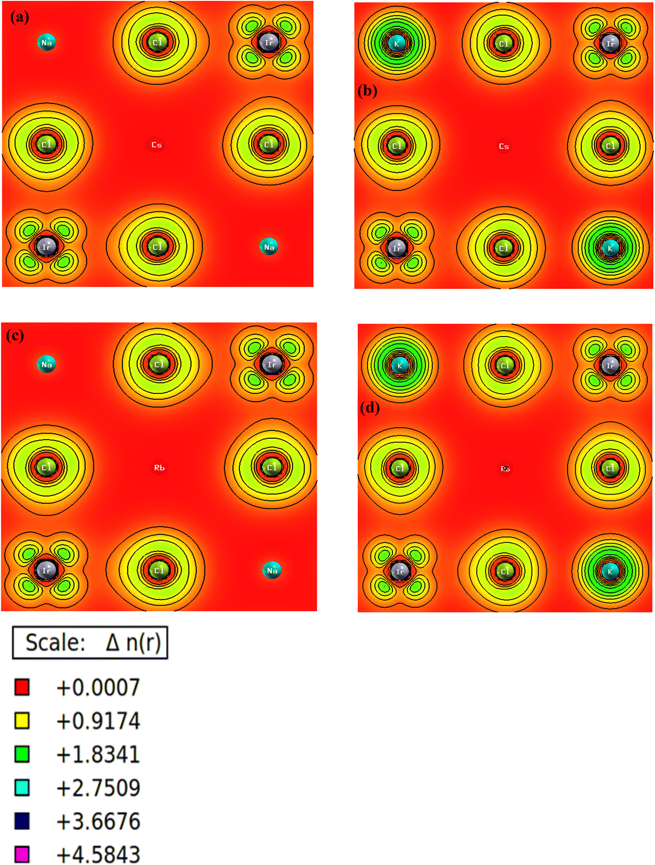 | ||
| Fig. 7 Contour plot of charge density of (a) Cs2NaIrCl6, (b) Cs2KIrCl6, (c) Rb2NaIrCl6, and (d) Rb2KIrCl6. | ||
3.4 Optical properties
The exceptional optical properties of lead-free (non-toxic) double perovskites, such as A2BIrCl6 (A = Cs, Rb; B = Na, K), and their potential applications in photovoltaic and optoelectronic devices have attracted significant attention. To evaluate the optical behaviour of these compounds, the dielectric function, ε(ω), is computed. It is expressed as ε(ω) = ε1(ω) + iε2(ω), where ε1(ω) and ε2(ω) represent the real and imaginary parts of the dielectric function, respectively.55–57 The real part ε1(ω) is calculated using the Kramers–Kronig relation:
 | (7) |
The imaginary part ε2(ω) is determined from the momentum matrix elements of the occupied and unoccupied wave functions: 58,59
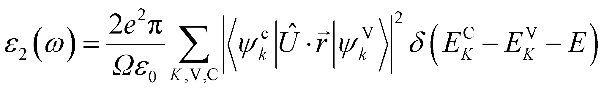 | (8) |
In this equation, ω is the photon frequency, ψck and ψVk are the wave functions of conduction and valence bands at wave vector k, e is the electronic charge, Ω is the unit cell volume, and Û is the unit vector along the electric field polarization. The delta function δ ensures energy and momentum conservation during transitions between electronic states. The energies ECK and EVK correspond to the conduction and valence band states at k, respectively.
The dielectric function is a crucial parameter that influences the charge-carrier recombination rate,60 providing a clear understanding of the efficiency of optoelectronic devices.61 Materials with higher static dielectric constants generally exhibit lower recombination rates, which enhances device performance. The real (ε1(ω)) and imaginary (ε2(ω)) components of the dielectric constant of A2BIrCl6 (A = Cs, Rb; B = Na, K) are depicted in Fig. 8a and b, respectively. The static dielectric function, ε1(0), for the investigated double perovskites is summarized as follows: ε1(0) = 2.78 for Cs2NaIrCl6, ε1(0) = 2.77 for Cs2KIrCl6, ε1(0) = 2.65 for Rb2NaIrCl6, and ε1(0) = 2.68 for Rb2KIrCl6. The relatively high ε1(0) values correspond to the materials' smaller band gaps, which are advantageous for reducing carrier recombination rates and enhancing optoelectronic device performance.62 As photon energy increases, ε1(ω) reaches its maximum value and then begins to decline, eventually attaining negative values. This signifies a transition from dielectric to metallic-like behavior. The crossover to negative ε1(ω) values occurs at higher photon energies, indicating the energy threshold beyond which the materials lose their dielectric properties. This behavior demonstrates that A2BIrCl6 (A = Cs, Rb; B = Na, K) acts as a dielectric material up to the specified energy limits, making it suitable for optoelectronic applications within this energy range.
 | ||
| Fig. 8 (a) ε1(ω): the real part of the dielectric constant, (b) ε2(ω): imaginary part of the dielectric constant, (c) n(ω): refractive index and (d) k(ω): extinction coefficient, (e) I(ω): absorption coefficient, (f) σ(ω): real optical conductivity, (g) R(ω): optical reflectivity, and (h) L(ω): loss function for studied compounds. | ||
The imaginary part of the dielectric function, ε2(ω), provides valuable insight into the electronic transitions between the valence and conduction bands. By examining ε2(ω), one can relate these transitions to the band structure of A2BIrCl6 (A = Cs, Rb; B = Na, K). As depicted in Fig. 8(b), the values of ε2(ω) remain negligible until reaching the band gap energy of each compound. At this point, significant peaks emerge, corresponding to the allowed transitions across the band gap. For Cs2NaIrCl6, Cs2KIrCl6, Rb2NaIrCl6, and Rb2KIrCl6, the notable peaks in ε2(ω) arise as the photon energy surpasses the band gap, reflecting strong optical transitions. The peaks' locations correspond to prominent transitions involving Ir 5d and Cl 3p orbitals, which dominate the conduction and valence band states. The precise energy positions of these peaks highlight the interplay between the electronic structure and optical properties of the double perovskites, confirming the direct band gap nature of these compounds.
Fig. 8(c) displays the fluctuations of refractive index n(ω). The refractive index n(ω), which is directly related to ε1(0) as  , 63 is shown in Fig. 8(c). The behaviour of ε1(ω) and n(ω) as functions of photon energy provides further insight into the dielectric properties of these materials. The static dielectric constants (ε1(0)) and refractive indices (n(0)) indicate that Cs2NaIrCl6 and Cs2KIrCl6 exhibit slightly higher dielectric and refractive properties compared to their Rb-based counterparts, consistent with their lower band gaps. For A2BIrCl6 (A = Cs, Rb; B = Na, K), the n(0) values range between 1.63 and 1.67, while the maximum n(ω) reaches approximately 2.4. These values indicate the dielectric behaviour of these materials and suggest their suitability for photovoltaic applications. The moderate n(0) values (between 1 and 2) and the maximum n(ω) values observed further confirm their potential for efficient light energy dispersion and absorption, essential characteristics for optoelectronic and energy-harvesting devices. The extinction coefficient, k(ω), quantifies the attenuation of electromagnetic radiation as it passes through a material. As shown in Fig. 8(d), the computed k(ω) values for A2BIrCl6 (A = Cs, Rb; B = Na, K) follow a trend similar to the imaginary part of the dielectric function, ε2(ω). This correlation highlights the direct relationship between optical absorption and k(ω), as ε2(ω) represents the material's ability to absorb energy from incident photons.
The Fig. 8(e) presents the absorption coefficient (α) as a function of photon energy (E) for A2BIrCl6 (A = Cs, Rb; B = Na, K) compounds. The absorption coefficient is a measure of how strongly a material absorbs light at a given energy. The absence of an electronic transition across the valence band to the conduction band was seen at incoming energy levels below the bandgap energy.
The optical conductivity σ(ω) for A2BIrCl6 (A = Cs, Rb; B = Na, K) is depicted in Fig. 8(f). As seen, the optical conductivity does not initiate at zero photon energy, a characteristic typical of semiconducting materials. Instead, the conductivity begins at specific photon energy thresholds, reflecting the materials' electronic band structures. For the compounds Cs2NaIrCl6, Cs2KIrCl6, Rb2NaIrCl6, and Rb2KIrCl6, the optical conductivity demonstrates distinct trends across the photon energy range. The conductivity increases with photon energy, exhibiting peaks that align well with the electronic transitions predicted by band structure calculations. These peaks correspond to photon-induced excitations from the valence band to the conduction band.
The reflectivity (R) spectra for A2BIrCl6 (A = Cs, Rb; B = Na, K) are shown in Fig. 8(g), highlighting the optical response of these semiconducting compounds. At zero photon energy, the calculated static reflectivity values R(0) is consistent across all compounds, as summarized in Table 4. Specifically, the values for R(0) are 6% for all compounds.
| DP | ε1(0) | n(0) | R(0) |
|---|---|---|---|
| Cs2NaIrCl6 | 2.78 | 1.67 | 0.06 |
| Cs2KIrCl6 | 2.77 | 1.66 | 0.06 |
| Rb2NaIrCl6 | 2.65 | 1.63 | 0.06 |
| Rb2KIrCl6 | 2.68 | 1.64 | 0.06 |
The Fig. 8(f) depicts the loss function, L(ω), as a function of photon energy for A2BIrCl6 (A = Cs, Rb; B = Na, K). The loss function represents the energy loss of a fast electron traversing the material, and its peaks correspond to the plasmon resonance frequencies, which are indicative of collective oscillations of the electron density. The most notable peaks for all compounds are observed between 4.5 eV and 6 eV. These peaks signify the plasmon resonance frequencies and correspond to the materials' characteristic energy loss due to plasmon excitation. Among the compounds, Rb2NaIrCl6 exhibits a slightly higher loss peak compared to the others. At photon energies below 4 eV, L(ω) remains low, suggesting minimal energy loss due to electronic interactions in this range. This property makes these materials promising candidates for photovoltaic applications, where efficient light harvesting is crucial.64 After the prominent peaks, L(ω) gradually decreases with increasing photon energy, indicating reduced plasmonic activity at higher photon energies. The compounds with higher ε1(0) (static dielectric constant) and lower band gaps tend to exhibit stronger and sharper plasmon peaks. This relationship correlates with the higher electron density contributing to the plasmon resonance.
3.5 Mechanical properties
Elastic constants are vital for understanding the mechanical behavior, stiffness, and stability of materials. For cubic systems like A2BIrCl6 (A = Cs, Rb; B = Na, K), only three independent elastic constants, C11, C12, and C44, are relevant. These constants are crucial in evaluating material properties like brittleness, malleability, and anisotropy. Using finite strain theory,65 the mechanical properties of A2BIrCl6 (A = Cs, Rb; B = Na, K) have been analyzed, providing insights into the compound's stability and response under applied forces, essential for potential engineering applications.The mechanical stability of Cs2NaIrCl6, Cs2KIrCl6, Rb2NaIrCl6, and Rb2KIrCl6 is confirmed by meeting the Born stability criteria66 as shown in Table 5. The calculated elastic constants indicate mechanical robustness, with Cs2NaIrCl6 and Rb2NaIrCl6 showing higher values of C11 − C12, indicating greater stiffness. Similarly, the high C11 + 2C12 values for these compounds suggest strong resistance to deformation. The lower C44 for Rb2KIrCl6 indicates relatively reduced shear resistance compared to the others. The Cauchy pressure (CP = C12 − C44) is a key indicator of material brittleness and ductility. A positive CP suggests ductility, while a negative CP indicates brittleness. The calculated CP values for A2BIrCl6 (A = Cs, Rb; B = Na, K) compounds are all negative are enlisted in Table 5. These results confirm their brittle nature, with Cs2KIrCl6 being the most brittle.
| Parameters | Cs2NaIrCl6 | Cs2KIrCl6 | Rb2NaIrCl6 | Rb2KIrCl6 | |
|---|---|---|---|---|---|
| Born stability | C11 (GPa) | 86.02 | 75.72 | 89.73 | 79.74 |
| C12 (GPa) | 15.40 | 9.49 | 13.58 | 8.17 | |
| C44 (GPa) | 19.44 | 14.97 | 17.17 | 9.64 | |
| C11 − C12 (GPa) | 70.62 | 66.23 | 76.15 | 71.57 | |
| C11 + 2C12 (GPa) | 116.82 | 94.70 | 116.89 | 96.08 | |
| Cauchy pressure, CP (GPa) | −4.04 | −5.48 | −3.59 | −1.47 | |
| Bulk modulus, B (GPa) | 38.94 | 31.57 | 38.96 | 32.03 | |
| Shear modulus, G (GPa) | 24.74 | 20.70 | 23.77 | 20.10 | |
| Young modulus, Y (GPa) | 61.26 | 50.96 | 59.26 | 43.04 | |
| Poisson's ratio, ν | 0.24 | 0.23 | 0.25 | 0.24 | |
| Pugh's ratio, B/G | 1.57 | 1.53 | 1.64 | 1.59 | |
| Zener anisotropy index, AZ | 0.55 | 0.45 | 0.45 | 0.27 | |
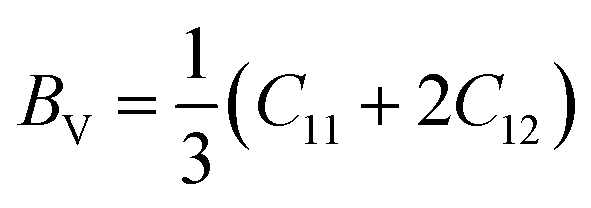
The mechanical properties of A2BIrCl6 (A = Cs, Rb; B = Na, K) are evaluated using estimated elastic constants, summarized in Table 5. The bulk modulus (B) measures the material's resistance to compression and is calculated using the formula:67
 | (9) |
The shear modulus (G), Young's modulus (E), Poisson's ratio (ν), and other properties are computed using the Voigt–Reuss approach. The Voigt and Reuss methods for determining the moduli are given by:68,69
 | (10) |
 | (11) |
 | (12) |
 | (13) |
The final values of B and G are obtained by averaging the Voigt and Reuss results:
 | (14) |
 | (15) |
Subsequently, Young's modulus (E) and Poisson's ratio (ν) are determined by the expressions:70,71
 | (16) |
 | (17) |
The estimated bulk moduli of A2BIrCl6 (A = Cs, Rb; B = Na, K) compounds, shown in Table 5, indicate that these materials are soft. Comparing the bulk modulus (B) with the shear modulus (G) reveals that for all compounds, B > G, suggesting that the mechanical strength is more influenced by shearing strain than volume strain. The bulk modulus is closely related to a material's atomic bond strength, as it inversely correlates with the unit cell volume and is linked to the cohesive or binding energy.72,73 From Table 5, it is evident that Cs2KIrCl6 exhibits the highest atomic bonding strength, surpassing the other compounds in terms of its bulk modulus value (31.57 GPa), implying stronger atomic interactions in this compound compared to the others. The stiffness of a material is described by its Young's modulus (E), where a higher value indicates greater stiffness. In Table 5, Cs2NaIrCl6 has the highest Young's modulus (61.26 GPa), making it the stiffest among the compounds, while Rb2KIrCl6 has the lowest E value (43.04 GPa), indicating it is more flexible. The Young's modulus is critical for analyzing thermal shock resistance (R), as the critical R value is inversely proportional to E.74 Thus, materials with a low E value, such as Rb2KIrCl6, exhibit higher thermal shock resistance compared to those with a higher E value like Cs2NaIrCl6.
Pugh's ratio (B/G) and Poisson's ratio (ν) are important indicators of a material's ductility or brittleness. For the compounds in Table 5, the Poisson's ratio values range from 0.23 to 0.25, while the Pugh's ratio ranges from 1.53 to 1.64. According to Pugh's criterion, a material is considered ductile if both ν > 0.26 and B/G > 1.75.67,75 Based on these criteria, all the titled compounds are classified as brittle.
The Zener anisotropy index (AZ) is a key parameter used to understand the isotropy and anisotropy of a material. It is calculated using the equation:75
 | (18) |
3.6 Thermodynamic properties
The thermodynamic properties of A2BIrCl6 (A = Cs, Rb; B = Na, K) perovskites, including density (ρ), sound velocities (vl, vt, vm), Debye temperature (θD), melting temperature (Tm), minimum thermal conductivity (kmin), and lattice thermal conductivity (KL) are presented in Table 6. The methodology for these calculations is detailed in ref. 73 and 78. The Debye temperature, θD, represents the highest normal mode of vibration in a crystal and correlates with material hardness and thermal conductivity. For most crystals, the Debye temperature (θD) typically ranges between 200–400 K.79 The estimated θD values for A2BIrCl6 (A = Cs, Rb; B = Na, K), as shown in Table 6, fall within this range. The values of θD range from 234.49 K (Rb2KIrCl6) to 276.67 K (Rb2NaIrCl6), indicating that all compounds are soft with low thermal conductivity. Rb2NaIrCl6 exhibits the highest θD, suggesting stronger bonding and greater hardness compared to others. Density (ρ) varies from 3.67 kg m−3 (Rb2KIrCl6) to 4.41 kg m−3 (Cs2NaIrCl6), while sound velocities (vl, vt, vm) are consistent with the calculated Debye temperatures. These findings provide valuable insights into the thermal and mechanical behaviour of these compounds for further research.| Parameters | Cs2NaIrCl6 | Cs2KIrCl6 | Rb2NaIrCl6 | Rb2KIrCl6 |
|---|---|---|---|---|
| ρ × 103 (kg m−3) | 4.41 | 4.12 | 3.95 | 3.67 |
| vl (m s−1) | 4037.75 | 3794.49 | 4235.57 | 3851.50 |
| vt (m s−1) | 2368.22 | 2244.38 | 2456.71 | 2142.20 |
| vm (m s−1) | 2625.46 | 2486.22 | 2726.31 | 2385.66 |
| θD (K) | 263.48 | 241.82 | 276.67 | 234.49 |
| Tm ± 300 (K) | 1061.35 | 1000.50 | 1083.31 | 1024.29 |
| M (kg mole−1) | 0.69 | 0.71 | 0.60 | 0.61 |
| Kmin (W m−1 K−1) | 0.41 | 0.37 | 0.44 | 0.36 |
| γ | 1.45 | 1.41 | 1.50 | 1.65 |
| KL (W m−1 K−1) | 1.64 | 1.43 | 1.51 | 0.78 |
The melting temperature (Tm) and minimum thermal conductivity (kmin) of A2BIrCl6 (A = Cs, Rb; B = Na, K) are shown in Table 6. The phonon mean free path has a strong influence on the lattice thermal conductivity. The lowest possible thermal conductivity may be attained if the phonon mean free path is like the interatomic distance. The calculated Tm values range from 1000.50 K (Cs2KIrCl6) to 1083.31 K (Rb2NaIrCl6), with Rb2NaIrCl6 having the highest melting point, suggesting stronger atomic interactions. The kmin values vary from 0.36 W m−1 K−1 (Rb2KIrCl6) to 0.44 W m−1 K−1 (Rb2NaIrCl6), indicating poor thermal conductivity across all compounds. The molar mass (M) ranges from 0.60 kg mole−1 (Rb2NaIrCl6) to 0.71 kg mole−1 (Cs2KIrCl6), aligning with the observed thermal properties. These findings highlight the compounds' low thermal conductivity and melting temperatures.
The lattice thermal conductivity (KL) is crucial for evaluating thermoelectric properties and the efficiency of energy conversion in thermoelectric materials, especially under high-temperature applications. Low KL is a prerequisite for materials intended for thermal insulation and thermoelectric devices.80,81 Weak chemical bonding leads to strong lattice anharmonicity, which is closely linked to the Grüneisen parameter (γ) and affects thermal transport by enhancing phonon scattering. At elevated temperatures, increased anharmonicity reduces phonon contribution to thermal conductivity. The parameters for A2BIrCl6 (A = Cs, Rb; B = Na, K) perovskites, shown in Table 6, indicate that KL ranges from 0.78 W m−1 K−1 (Rb2KIrCl6) to 1.64 W m−1 K−1 (Cs2NaIrCl6). The Grüneisen parameter (γ) varies from 1.41 (Cs2KIrCl6) to 1.65 (Rb2KIrCl6), highlighting significant anharmonicity.
The thermodynamic potential of a system provides an in-depth view of its optimal behavior. By applying the quasiharmonic method 82 and the computed phonon density of states, we calculate the thermodynamic potential for A2BIrCl6 (A = Cs, Rb; B = Na, K). The parameters considered include entropy (S), internal energy (E), Helmholtz free energy (F), and specific heat (Cv), which are calculated using the following equations.83
 | (19) |
 | (20) |
 | (21) |
 | (22) |
In these equations, kB refers to the Boltzmann constant, N stands for Avogadro's number, n indicates the number of atoms in each unit cell, w denotes the phonon frequency, wmax is the maximum phonon frequency, and g(w) is the normalized density of states for phonons. With,
 | (23) |
Fig. 9 and 10 display the computed values of F, E, S, and Cv across a temperature range from 0 K to 1000 K. The Helmholtz free energy (F) of A2BIrCl6 (A = Cs, Rb; B = Na, K) is shown in Fig. 10, displaying a steady decrease with increasing temperature. The reduction in free energy is a natural phenomenon, where it becomes more negative as the process progresses. The data indicates that enthalpy, entropy, and heat capacity increase as temperature rises.
 | ||
| Fig. 9 The temperature-dependent variations of the computed thermodynamic parameters enthalpy (E), free energy (F), and entropy (S) for A2BIrCl6 (A = Cs, Rb; B = Na, K) at zero pressure. | ||
 | ||
| Fig. 10 The temperature-dependent variations of the computed thermodynamic parameters heat capacity and Debye temperature for A2BIrCl6 (A = Cs, Rb; B = Na, K) at zero pressure. | ||
The thermodynamic behavior of solids can be understood by analyzing their specific heat, which indicates their heat retention ability. Our findings reveal that the heat capacity of the material increases more prominently compared to its enthalpy and entropy, indicating that the A2BIrCl6 (A = Cs, Rb; B = Na, K) systems are highly responsive to temperature changes. As the temperature rises, the heat capacity gradually increases, eventually stabilizing at approximately 58 (Cs2NaIrCl6), 57 (Cs2KIrCl6), 58 (Rb2NaIrCl6), and 57 (Rb2KIrCl6) cal per cell K. This value is frequently identified as the Dulong–Petit limit.84 The Debye temperature (θD) serves as a vital parameter in numerous thermophysical properties. Higher (θD) values usually correlate with more robust atomic bonding and a greater phonon role in heat conduction. For all the compounds examined, the Debye temperature grows with increasing temperature. The maximum Debye temperature for all studied compounds is around 450 K at 1000 K.
4. Conclusion
This study presents the first exploration of four novel double halide perovskites, A2BIrCl6 (A = Cs, Rb; B = Na, K), and investigates their structural, electronic, optical, mechanical, and thermo-physical properties, providing essential insights into their potential applications. The stability of the cubic phase structure is validated through several criteria, including tolerance factors between 0.88 and 0.98, as well as octahedral factors ranging from 0.47 to 0.57. The assessment of their thermodynamic stability and dynamic equilibrium was based on their positive phonon dispersion, along with negative formation and binding energies. These materials exhibit semiconducting properties, with a direct band gap identified at the X–X symmetry k-points. The energy band gaps calculated for Cs2NaIrCl6, Cs2KIrCl6, Rb2NaIrCl6, and Rb2KIrCl6 are 1.927 eV, 1.991 eV, 2.025 eV, and 2.102 eV, respectively, making them highly suitable for use in solar cell and optoelectronics applications. Additionally, the investigation of their optical properties highlighted significant visible light absorption (up to 104 cm−1) and minimal reflectivity, pointing to their potential as highly effective absorber layers in solar cell applications. The elastic constants Poisson's ratio, Pugh's ratio, and Cauchy pressure obtained from the study suggest that the perovskites analyzed exhibit mechanical stability, though they demonstrate brittle characteristics. The thermodynamic characteristics of A2BIrCl6 (A = Cs, Rb; B = Na, K), including specific heat, Helmholtz free energy, internal energy, entropy, Debye temperature, melting point, minimum thermal conductivity, lattice thermal conductivity, and the Grüneisen parameter, indicate their thermodynamic stability. These findings indicate that the titled double perovskite materials are potential candidates for optoelectronic and photovoltaic applications.Data availability
The data supporting this study's findings are available from the corresponding author upon reasonable request.Author contributions
Investigation was led by Md. Tarekuzzaman, who also contributed to methodology development, data curation, conceptualization, and drafting of the original manuscript. Nazmul Shahadath participated in formal analysis, methodology development, data curation, and manuscript review and editing. Formal analysis was conducted by Mufrat Montasir, who also provided software support, contributed to conceptualization, and participated in manuscript review and editing. O. Alsalmi provided validation and conducted formal analysis. M. H. Mia engaged in formal analysis, contributed to methodology development, data curation, and manuscript review and editing. Hmoud Al-Dmour provided validation and conducted formal analysis. Md. Rasheduzzaman conducted formal analysis, provided validation, and participated in manuscript review and editing. Md. Zahid Hasan conducted formal analysis, provided validation, supervised the study, and participated in manuscript review and editing.Conflicts of interest
There is no conflict to declare.Acknowledgements
The authors extend their appreciation to Umm Al-Qura University, Saudi Arabia for funding this research work through grant number: 25UQU4300099GSSR01. Funding statement: this research work was funded by Umm Al-Qura University, Saudi Arabia under grant number: 25UQU4300099GSSR01.References
- W.-J. Yin, B. Weng, J. Ge, Q. Sun, Z. Li and Y. Yan, Oxide Perovskites, Double Perovskites and Derivatives for Electrocatalysis, Photocatalysis, and Photovoltaics, Energy Environ. Sci., 2019, 12(2), 442–462 RSC.
- C. Bogmans, et al., Energy, Efficiency Gains and Economic Development: When Will Global Energy Demand Saturate?, 2020 Search PubMed.
- W.-J. Yin, J.-H. Yang, J. Kang, Y. Yan and S.-H. Wei, Halide Perovskite Materials for Solar Cells: A Theoretical Review, J. Mater. Chem. A, 2015, 3(17), 8926–8942 RSC.
- J. Song, J. Li, X. Li, L. Xu, Y. Dong and H. Zeng, Quantum Dot Light-Emitting Diodes Based on Inorganic Perovskite Cesium Lead Halides (CsPbX3), Adv. Mater., 2015, 27(44), 7162–7167 CrossRef CAS PubMed.
- S. A. Veldhuis, P. P. Boix, N. Yantara, M. Li, T. C. Sum, N. Mathews and S. G. Mhaisalkar, Perovskite Materials for Light-Emitting Diodes and Lasers, Adv. Mater., 2016, 28(32), 6804–6834 CrossRef CAS PubMed.
- S. M. H. Qaid, Q. ul Ain, H. M. Ghaithan, I. Mursaleen, A. Ahmed Ali Ahmed and J. Munir, First-Principles Investigations on the Structural, Optoelectronic, Mechanical and Transport Properties of New Stable Lead-Free Double Perovskites Cs2BB′I6 (B = Ag/Rb, B′ = Bi/Ga) Halides, Mater. Sci. Eng. B, 2024, 301, 117176 CrossRef CAS.
- H. Murtaza, Q. ul Ain, J. Munir, H. M. Ghaithan, A. A. A. Ahmed and S. M. H. Qaid, Exploring the Optoelectronic Attributes, Thermoelectric and Photocatalytic Potential of Double Perovskites Cs2BB’H6 (B = Al, Na and B’=Tl, In): A DFT Study, Mater. Sci. Eng. B, 2024, 301, 117171 CrossRef CAS.
- H. Murtaza, J. Munir, H. M. Ghaithan, Q. ul Ain, A. A. A. Ahmed and S. M. H. Qaid, Scrutinize the Physical Attributes of Thermodynamically and Elastically Stable Double Perovskite Oxides Ba2CdXO6 (X = Mo, U) for Optoelectronics, Photocatalytic and Green Technology, Comput. Mater. Sci., 2024, 232, 112674 CrossRef CAS.
- Q. Mahmood, G. M. Mustafa, M. Morsi, H. Albalawi, T. H. Flemban, M. Hassan, H. Althib, M. I. Khan and T. Ghrib, Theoretical Investigations of Optoelectronic and Thermoelectric Properties of Halide Based Double Perovskite Halides: K2TeX6, Phys. Scr., 2021, 96(7), 075703 CrossRef CAS.
- L. Mao, S. M. L. Teicher, C. C. Stoumpos, R. M. Kennard, R. A. DeCrescent, G. Wu, J. A. Schuller, M. L. Chabinyc, A. K. Cheetham and R. Seshadri, Chemical and Structural Diversity of Hybrid Layered Double Perovskite Halides, J. Am. Chem. Soc., 2019, 141(48), 19099–19109 CrossRef CAS PubMed.
- S. M. H. Qaid, M. Jamil, J. Munir, H. M. Ghaithan, A. A. A. Ahmed and Q. ul. Ain, A Computational Insight into Rb2ASbX6 (A=Tl, Cu & X=I, Cl) Double Perovskites for Energy Storage and Optoelectronic Applications, Phys. Scr., 2023, 98(10), 105910 CrossRef CAS.
- M. T. Anderson, K. B. Greenwood, G. A. Taylor and K. R. Poeppelmeier, B-Cation Arrangements in Double Perovskites, Prog. Solid State Chem., 1993, 22(3), 197–233 CrossRef CAS.
- R. D. Nelson, K. Santra, Y. Wang, A. Hadi, J. W. Petrich and M. G. Panthani, Synthesis and Optical Properties of Ordered-Vacancy Perovskite Cesium Bismuth Halide Nanocrystals, Chem. Commun., 2018, 54(29), 3640–3643 RSC.
- L. A. Muscarella and E. M. Hutter, Halide Double-Perovskite Semiconductors beyond Photovoltaics, ACS Energy Lett., 2022, 7(6), 2128–2135 CrossRef CAS PubMed.
- N. J. Jeon, J. H. Noh, W. S. Yang, Y. C. Kim, S. Ryu, J. Seo and S. I. Seok, Compositional Engineering of Perovskite Materials for High-Performance Solar Cells, Nature, 2015, 517(7535), 476–480 CrossRef CAS PubMed.
- J. Munir, M. K. Iftikhar, M. I. Jamil, M. U. Din, T. Alshahrani, H. I. Elsaeedy and Q. Ain, Physical Properties of Elastically and Thermodynamically Stable Magnetic AcXO3 (X = Cr, Fe) Perovskite Oxides: A DFT Investigation, Phys. Scr., 2023, 98(6), 065513 CrossRef CAS.
- J. Munir, M. Mustafa, H. Naeem, M. Yousaf, E. F. El-Shamy and Q. Ain, Electronic Structure, Optical and Thermal Response of Lead-Free RbAuBr3 and RbAuBr4 Perovskites for Renewable Energy Applications, ECS J. Solid State Sci. Technol., 2022, 11(12), 123003 CrossRef CAS.
- S. A. Dar and B. Want, Direct Band Gap Double Perovskite Halide Cs2ScInCl6 for Optoelectronic Applications—A First Principle Study, Comput. Condens. Matter., 2022, 33, e00736 CrossRef.
- H. Zhou, Q. Chen, G. Li, S. Luo, T. Song, H.-S. Duan, Z. Hong, J. You, Y. Liu and Y. Yang, Interface Engineering of Highly Efficient Perovskite Solar Cells, Science, 2014, 345(6196), 542–546 CrossRef CAS PubMed.
- M. Saliba, T. Matsui, K. Domanski, J.-Y. Seo, A. Ummadisingu, S. M. Zakeeruddin, J.-P. Correa-Baena, W. R. Tress, A. Abate, A. Hagfeldt and M. Grätzel, Incorporation of Rubidium Cations into Perovskite Solar Cells Improves Photovoltaic Performance, Science, 2016, 354(6309), 206–209 CrossRef CAS PubMed.
- A. Al-Ashouri, E. Köhnen, B. Li, A. Magomedov, H. Hempel, P. Caprioglio, J. A. Márquez, A. B. Morales Vilches, E. Kasparavicius, J. A. Smith, N. Phung, D. Menzel, M. Grischek, L. Kegelmann, D. Skroblin, C. Gollwitzer, T. Malinauskas, M. Jošt, G. Matič, B. Rech, R. Schlatmann, M. Topič, L. Korte, A. Abate, B. Stannowski, D. Neher, M. Stolterfoht, T. Unold, V. Getautis and S. Albrecht, Monolithic Perovskite/Silicon Tandem Solar Cell with >29% Efficiency by Enhanced Hole Extraction, Science, 2020, 370(6522), 1300–1309 CrossRef CAS PubMed.
- S. De Wolf, J. Holovsky, S.-J. Moon, P. Löper, B. Niesen, M. Ledinsky, F.-J. Haug, J.-H. Yum and C. Ballif, Organometallic Halide Perovskites: Sharp Optical Absorption Edge and Its Relation to Photovoltaic Performance, J. Phys. Chem. Lett., 2014, 5(6), 1035–1039 CrossRef CAS PubMed.
- C. C. Stoumpos, C. D. Malliakas and M. G. Kanatzidis, Semiconducting Tin and Lead Iodide Perovskites with Organic Cations: Phase Transitions, High Mobilities, and Near-Infrared Photoluminescent Properties, Inorg. Chem., 2013, 52(15), 9019–9038 CrossRef CAS PubMed.
- O. A. Lozhkina, A. A. Murashkina, M. S. Elizarov, V. V. Shilovskikh, A. A. Zolotarev, Yu. V. Kapitonov, R. Kevorkyants, A. V. Emeline and T. Miyasaka, Microstructural Analysis and Optical Properties of the Halide Double Perovskite Cs2BiAgBr6 Single Crystals, Chem. Phys. Lett., 2018, 694, 18–22 CrossRef CAS.
- X.-G. Zhao, J.-H. Yang, Y. Fu, D. Yang, Q. Xu, L. Yu, S.-H. Wei and L. Zhang, Design of Lead-Free Inorganic Halide Perovskites for Solar Cells via Cation-Transmutation, J. Am. Chem. Soc., 2017, 139(7), 2630–2638 CrossRef CAS PubMed.
- E. T. McClure, M. R. Ball, W. Windl and P. M. Woodward, Cs2AgBiX6 (X = Br, Cl): New Visible Light Absorbing, Lead-Free Halide Perovskite Semiconductors, Chem. Mater., 2016, 28(5), 1348–1354 CrossRef CAS.
- A. J. Kale, R. Chaurasiya and A. Dixit, Inorganic Lead-Free Cs2AuBiCl6 Perovskite Absorber and Cu2O Hole Transport Material Based Single-Junction Solar Cells with 22.18% Power Conversion Efficiency, Adv. Theory Simul., 2021, 4(3), 2000224 CrossRef CAS.
- R. E. Brandt, R. C. Kurchin, R. L. Z. Hoye, J. R. Poindexter, M. W. B. Wilson, S. Sulekar, F. Lenahan, P. X. T. Yen, V. Stevanović, J. C. Nino, M. G. Bawendi and T. Buonassisi, Investigation of Bismuth Triiodide (BiI3) for Photovoltaic Applications, J. Phys. Chem. Lett., 2015, 6(21), 4297–4302 CrossRef CAS PubMed.
- G. Volonakis, A. A. Haghighirad, R. L. Milot, W. H. Sio, M. R. Filip, B. Wenger, M. B. Johnston, L. M. Herz, H. J. Snaith and F. Giustino, Cs2InAgCl6: A New Lead-Free Halide Double Perovskite with Direct Band Gap, J. Phys. Chem. Lett., 2017, 8(4), 772–778 CrossRef CAS PubMed.
- B. Nath, B. Pradhan and S. K. Panda, Optical Tunability of Lead Free Double Perovskite Cs2AgInCl6via Composition Variation, New J. Chem., 2020, 44(43), 18656–18661 RSC.
- B. Yang and K. Han, Charge-Carrier Dynamics of Lead-Free Halide Perovskite Nanocrystals, Acc. Chem. Res., 2019, 52(11), 3188–3198 CrossRef CAS PubMed.
- J. C. Dahl, W. T. Osowiecki, Y. Cai, J. K. Swabeck, Y. Bekenstein, M. Asta, E. M. Chan and A. P. Alivisatos, Probing the Stability and Band Gaps of Cs2AgInCl6 and Cs2AgSbCl6 Lead-Free Double Perovskite Nanocrystals, Chem. Mater., 2019, 31(9), 3134–3143 CrossRef CAS.
- M. G. B. Ashiq, Q. Mahmood, T. Zelai, O. Hakami, N. A. Kattan, H. Albalawi, A. I. Aljameel, S. Bouzgarrou, T. Ghrib and K. I. Hussein, The Narrow Band Bap Double Perovskites X2CuInCl6 (X = K, Rb, Cs) for Optoelectronics, and Thermoelectric Applications, Mater. Sci. Eng. B, 2023, 296, 116690 CrossRef CAS.
- D. Behera, B. Mohammed, S. Taieb, B. Mokhtar, S. Al-Qaisi and S. K. Mukherjee, First-Principle Investigations on Optoelectronics and Thermoelectric Properties of Lead-Free Rb2InSbX6 (X = Cl, Br) Double Perovskites: For Renewable Energy Applications, Eur. Phys. J. Plus, 2023, 138(6), 520 CrossRef CAS.
- A. Ayyaz, G. Murtaza, M. Shafiq, M. Qasim Shah, N. Sfina and S. Ali, Exploring Structural, Thermodynamic, Elastic, Electro-Optic, and Thermoelectric Characteristics of Double Perovskites Rb2XInBr6 (X = Na, K) for Photovoltaic Applications: A DFT Approach, Sol. Energy, 2023, 265, 112131 CrossRef CAS.
- M. Zia ur Rehman, S. A. M. Abdelmohsen, E. A. Mahmoud, M. U. Saeed, M. Idress, M. Shafiq, B. Amin and Y. Saeed, First Principles Study of Structural, Electronic, Elastic and Optical Properties of Cs2LiTlBr6 and Cs2NaTlBr6, Mater. Sci. Semicond. Process., 2022, 151, 106993 CrossRef CAS.
- S. H. Shah, P. song, T. Huang, S. Shakeel, S. Khan, M. W. Ashraf and G. Murtaza, Comprehensive Study of Structural, Elastic, Electronic, Optical, and Thermoelectric Properties of Rb2NaTlZ6 (Z = Cl, Br, and I) by DFT, Mater. Sci. Semicond. Process., 2024, 178, 108400 CrossRef CAS.
- H. Murtaza, Q. Ain, J. Munir, H. M. Ghaithan, M. Ali, A. A. Ali Ahmed, H. Qaid and S. M. H. Qaid, Tuning the Thermoelectric and Optoelectronic Attributes of Lead-Free Novel Fluoroperovskites Cs2BB’F6 (B = Rb, In, Na and B’=Ir, As, Rh): A First-Principles Investigation, J. Phys. Chem. Solids, 2024, 190, 111934 CrossRef CAS.
- P. Hohenberg and W. Kohn, Inhomogeneous Electron Gas, Phys. Rev., 1964, 136(3B), B864–B871 CrossRef.
- W. Kohn and L. J. Sham, Self-Consistent Equations Including Exchange and Correlation Effects, Phys. Rev., 1965, 140(4A), A1133–A1138 CrossRef.
- K. Schwarz, DFT Calculations of Solids with LAPW and WIEN2k, J. Solid State Chem., 2003, 176(2), 319–328 CrossRef CAS.
- J. P. Perdew, K. Burke and M. Ernzerhof, Generalized Gradient Approximation Made Simple, Phys. Rev. Lett., 1996, 77(18), 3865–3868 CrossRef CAS PubMed.
- F. D. Murnaghan, The Compressibility of Media under Extreme Pressures, Proc. Natl. Acad. Sci. U. S. A., 1944, 30(9), 244–247 CrossRef CAS PubMed.
- F. Tran and P. Blaha, Accurate Band Gaps of Semiconductors and Insulators with a Semilocal Exchange-Correlation Potential, Phys. Rev. Lett., 2009, 102(22), 226401 CrossRef PubMed.
- K. Momma and F. Izumi, VESTA 3 for Three-Dimensional Visualization of Crystal, Volumetric and Morphology Data, J. Appl. Crystallogr., 2011, 44(6), 1272–1276 CrossRef CAS.
- M. D. Segall, P. J. D. Lindan, M. J. Probert, C. J. Pickard, P. J. Hasnip, S. J. Clark and M. C. Payne, First-Principles Simulation: Ideas, Illustrations and the CASTEP Code, J. Phys.:Condens. Matter, 2002, 14(11), 2717 CrossRef CAS.
- I. Borriello, G. Cantele and D. Ninno, Ab Initio Investigation of Hybrid Organic-Inorganic Perovskites Based on Tin Halides, Phys. Rev. B:Condens. Matter Mater. Phys., 2008, 77(23), 235214 CrossRef.
- X. Du, D. He, H. Mei, Y. Zhong and N. Cheng, Insights on Electronic Structures, Elastic Features and Optical Properties of Mixed-Valence Double Perovskites Cs2Au2X6 (X=F, Cl, Br, I), Phys. Lett. A, 2020, 384(8), 126169 CrossRef CAS.
- V. M. Goldschmidt, Die Gesetze der Krystallochemie, Naturwissenschaften, 1926, 14(21), 477–485 CrossRef CAS.
- C. J. Bartel, C. Sutton, B. R. Goldsmith, R. Ouyang, C. B. Musgrave, L. M. Ghiringhelli and M. Scheffler, New Tolerance Factor to Predict the Stability of Perovskite Oxides and Halides, Sci. Adv., 2019, 5(2), eaav0693 CrossRef CAS PubMed.
- C. Li, X. Lu, W. Ding, L. Feng, Y. Gao and Z. Guo, Formability of ABX3 (X = F, Cl, Br, I) Halide Perovskites, Acta Crystallogr., Sect. B, 2008, 64(6), 702–707 CrossRef CAS.
- A. Togo and I. Tanaka, First Principles Phonon Calculations in Materials Science, Scr. Mater., 2015, 108, 1–5 CrossRef CAS.
- C. Kittel and P. McEuen, Introduction to Solid State Physics, John Wiley & Sons, 2018 Search PubMed.
- M. Wuttig, et al., Halide perovskites: Advanced photovoltaic materials empowered by a unique bonding mechanism, Adv. Funct. Mater., 2022, 32(2), 2110166 CrossRef CAS.
- A. A. Mubarak, The First-Principle Study of the Electronic, Optical and Thermoelectric Properties of XTiO3 (X = Ca, Sr and Ba) Compounds, Int. J. Mod. Phys. B, 2016, 30(20), 1650141 CrossRef CAS.
- K. E. Babu, et al., First-principles study of electronic structure and optical properties of cubic perovskite CsCaF3, Chin. Phys. Lett., 2012, 29(11), 117102 CrossRef.
- M. A. Green, Y. Jiang, A. M. Soufiani and A. Ho-Baillie, Optical Properties of Photovoltaic Organic–Inorganic Lead Halide Perovskites, J. Phys. Chem. Lett., 2015, 6(23), 4774–4785 CrossRef CAS PubMed.
- C. Ambrosch-Draxl and J. O. Sofo, Linear Optical Properties of Solids within the Full-Potential Linearized Augmented Planewave Method, Comput. Phys. Commun., 2006, 175(1), 1–14 CrossRef CAS.
- N. V. Smith, Photoelectron Energy Spectra and the Band Structures of the Noble Metals, Phys. Rev. B, 1971, 3(6), 1862–1878 CrossRef.
- X. Liu, B. Xie, C. Duan, Z. Wang, B. Fan, K. Zhang, B. Lin, F. J. M. Colberts, W. Ma, R. A. J. Janssen, F. Huang and Y. Cao, A High Dielectric Constant Non-Fullerene Acceptor for Efficient Bulk-Heterojunction Organic Solar Cells, J. Mater. Chem. A, 2018, 6(2), 395–403 RSC.
- S. Saha, T. P. Sinha and A. Mookerjee, Electronic Structure, Chemical Bonding, and Optical Properties of Paraelectric ${\mathrm{BaTiO}}_{3, Phys. Rev. B:Condens. Matter Mater. Phys., 2000, 62(13), 8828–8834 CrossRef CAS.
- S. Zuhair Abbas Shah, S. Niaz, T. Nasir and S. M. Ramay, Exploring the Structural, Phononic, Electronic, Magnetic, Optical, and Thermoelectric Properties of Pb-Free Vanadium-Based Double Perovskites Using the First-Principles Approach for Optoelectronic and Thermoelectric Applications, Sol. Energy, 2022, 240, 27–37 CrossRef CAS.
- G. Murtaza, A. A. AlObaid, T. I. Al-Muhimeed, S. Al-Qaisi, A. Rehman, H. H. Hegazy, G. Nazir, M. Morsi and Q. Mahmood, Tailoring of Band Gap to Tune the Optical and Thermoelectric Properties of Sr1-xBaxSnO3 Stannates for Clean Energy; Probed by DFT, Chem. Phys., 2021, 551, 111322 CrossRef.
- S. Z. A. Shah, A. Afzal, F. Khan, S. Zafar, J. Sifuna, A. A. Nassani, S. U. Asif and Z. Abbas, Small Band Gap Pb-Free Double Perovskites X2NaSbBr6 (X=Na, Li): A Study of the Stabilities, Opto-Electronic and Thermoelectric Aspects from the First-Principles Approach, Comput. Condens. Matter., 2025, 42, e01001 CrossRef.
- F. D. Murnaghan, Finite Deformations of an Elastic Solid, Am. J. Math., 1937, 59(2), 235–260 CrossRef.
- M. Born, On the Stability of Crystal Lattices. I, Math. Proc. Camb. Philos. Soc., 1940, 36(2), 160–172 CrossRef CAS.
- I. N. Frantsevich, Elastic Constants and Elastic Moduli of Metals and Insulators, 1982 Search PubMed.
- A. Reuss, Berechnung Der Fließgrenze von Mischkristallen Auf Grund Der Plastizitätsbedingung Für Einkristalle, J. Appl. Math. Mech., 1929, 9(1), 49–58 CAS.
- R. Hill, The Elastic Behaviour of a Crystalline Aggregate, Proc. Phys. Soc. Sect. A, 1952, 65(5), 349 CrossRef.
- M. Al-Fahdi, A. Rodriguez, T. Ouyang and M. Hu, High-Throughput Computation of New Carbon Allotropes with Diverse Hybridization and Ultrahigh Hardness, Crystals, 2021, 11(7), 783 CrossRef CAS.
- G. Vaitheeswaran, V. Kanchana, A. Svane and A. Delin, Elastic Properties of MgCNi3—a Superconducting Perovskite, J. Phys.:Condens. Matter, 2007, 19(32), 326214 CrossRef.
- D. G. Clerc and H. M. Ledbetter, Mechanical Hardness: A Semiempirical Theory Based on Screened Electrostatics and Elastic Shear, J. Phys. Chem. Solids, 1998, 59(6), 1071–1095 CrossRef CAS.
- M. A. Khatun, M. H. Mia, M. A. Hossain, F. Parvin and A. K. M. A. Islam, Optical and Thermoelectric Properties of Layer Structured Ba2XS4 (X = Zr, Hf) for Energy Harvesting Applications, J. Phys. Chem. Solids, 2025, 196, 112381 CrossRef CAS.
- X. Wang, H. Xiang, X. Sun, J. Liu, F. Hou and Y. Zhou, Mechanical Properties and Damage Tolerance of Bulk Yb3Al5O12 Ceramic, J. Mater. Sci. Technol., 2015, 31(4), 369–374 CrossRef CAS.
- S. F. Pugh, XCII. Relations between the Elastic Moduli and the Plastic Properties of Polycrystalline Pure Metals, Lond. Edinb. Dublin Philos. Mag. J. Sci., 1954, 45(367), 823–843 CrossRef CAS.
- H. Ledbetter and A. Migliori, A General Elastic-Anisotropy Measure, J. Appl. Phys., 2006, 100(6), 063516 CrossRef.
- S. I. Ranganathan and M. Ostoja-Starzewski, Universal Elastic Anisotropy Index, Phys. Rev. Lett., 2008, 101(5), 055504 CrossRef.
- M. H. K. Rubel, M. A. Hossain, M. K. Hossain, K. M. Hossain, A. A. Khatun, M. M. Rahaman, Md. Ferdous Rahman, M. M. Hossain and J. Hossain, First-Principles Calculations to Investigate Structural, Elastic, Electronic, Thermodynamic, and Thermoelectric Properties of CaPd3B4O12 (B = Ti, V) Perovskites, Results Phys., 2022, 42, 105977 CrossRef.
- O. L. Anderson, A Simplified Method for Calculating the Debye Temperature from Elastic Constants, J. Phys. Chem. Solids, 1963, 24(7), 909–917 CrossRef CAS.
- W. Lee, H. Li, A. B. Wong, D. Zhang, M. Lai, Y. Yu, Q. Kong, E. Lin, J. J. Urban, J. C. Grossman and P. Yang, Ultralow Thermal Conductivity in All-Inorganic Halide Perovskites, Proc. Natl. Acad. Sci. U. S. A., 2017, 114(33), 8693–8697 CrossRef CAS PubMed.
- Q. Yan and M. G. Kanatzidis, High-Performance Thermoelectrics and Challenges for Practical Devices, Nat. Mater., 2022, 21(5), 503–513 CrossRef CAS PubMed.
- C. Lee and X. Gonze, Ab Initio Calculation of the Thermodynamic Properties and Atomic Temperature Factors of ${\mathrm{SiO}}_{2}$ \ensuremath{\alpha}-Quartz and Stishovite, Phys. Rev. B:Condens. Matter Mater. Phys., 1995, 51(13), 8610–8613 CrossRef CAS PubMed.
- S. Baroni, S. de Gironcoli, A. Dal Corso and P. Giannozzi, Phonons and Related Crystal Properties from Density-Functional Perturbation Theory, Rev. Mod. Phys., 2001, 73(2), 515–562 CrossRef CAS.
- D. Wu, S. Huang, D. Feng, B. Li, Y. Chen, J. Zhang and J. He, Revisiting AgCrSe2 as a Promising Thermoelectric Material, Phys. Chem. Chem. Phys., 2016, 18(34), 23872–23878 RSC.
Footnote |
| † Electronic supplementary information (ESI) available. See DOI: https://doi.org/10.1039/d5ra01748c |
| This journal is © The Royal Society of Chemistry 2025 |