
 Open Access Article
 This Open Access Article is licensed under a
 Creative Commons Attribution 3.0 Unported Licence
Tailoring morphological and electrical properties of nanoplate-ZnO varistors via sintering temperature†
Huy Nguyen Trungab,
Trang Nguyen Vana,
Kieu Anh Vo Thia,
Hong Cao Thia,
Xuyen Nguyen Thia,
Tuan Anh Nguyenb,
Tuan Anh Nguyena,
Lam Tran Daia,
Chinh Tran Vanc,
Duy Lai Vand,
Duong La Duc *c and
Tham Do Quang*ab
*c and
Tham Do Quang*ab
aInstitute for Tropical Technology, Vietnam Academy of Science and Technology, 18 Hoang Quoc Viet Street, Cau Giay District, Hanoi City, Vietnam. E-mail: dqtham@itt.vast.vn
bGraduate University of Science and Technology (GUST), Vietnam Academy of Science and Technology, 18 Hoang Quoc Viet Street, Cau Giay, Hanoi, Vietnam
cInstitute of Chemistry and Materials, 17 Hoang Sam, Nghia Do, Cau Giay, Hanoi, Vietnam. E-mail: duc.duong.la@gmail.com
dInstitute of Materials Science, Vietnam Academy of Science and Technology, 18 Hoang Quoc Viet Street, Cau Giay District, Hanoi City, Vietnam
First published on 12th June 2025
Abstract
In this study, ZnO nanoplates (crystallite size: 100 nm, thickness: 15 nm) were synthesized via a hydrothermal route. Varistors were then fabricated using these ZnO nanoplates incorporated with five oxide dopants (Bi2O3, Sb2O3, MnO2, Co3O4, and Cr2O3) and sintered at 1000, 1100, and 1200 °C. A control varistor sample using micro-sized ZnO was also prepared. The effects of sintering temperature on the structural, mechanical, and electrical properties of ZnO-based varistors were systematically studied. Increasing the sintering temperature from 1000 °C to 1200 °C enlarged the grain size (1.7–6.8 μm), enhanced hardness (200–280 HV), and resulted in 17–19% shrinkage. At 1100 °C, the varistor achieved a balance of high nonlinearity (α = 48.5), low leakage current (JL = 9.7 μA cm−2), and high breakdown threshold (Eb = 689 V mm−1). Impedance analysis showed a resistive–capacitive transition at higher frequencies, while grain boundary resistivity at low frequencies (106.5–108 Ω m) aligned with DC resistivity at the low applied electric fields. These results highlight the advantages of ZnO nanoplates in enhancing the electrical performance of varistors, making them promising for high-voltage applications.
Introduction
Varistors, or voltage-dependent resistors, are widely used in both low-power electronic devices and high-power electrical distribution systems to protect circuits from transient voltage surges through their nonlinear current–voltage (I–V) characteristics.1–5 Various materials such as SiC, TiO2, SnO2, WO3, and SrTiO3 have been explored as base materials for varistors with nonlinear voltage–current (V–I) characteristics. SiC varistors were among the earliest used but have low nonlinearity coefficient (α < 10), and require internal spark gaps due to high leakage current. TiO2-based varistors offer high dielectric constant and surge absorption capacity, but suffer from low breakdown voltage and nonlinearity, limiting them in low-voltage surge protection applications. WO3-based varistors also operate at low-voltage applications due to their very low breakdown voltage (6–10 V mm−1). They are suitable for ceramic capacitor. SrTiO3 offers advantages for low-voltage varistor-capacitor dual function, owing to its high dielectric constant and nonlinear behavior. SnO2-based varistors offer good thermal stability and nonlinearity but still exhibit a higher residual voltage ratio. However, they exhibit relative higher residual voltage ratio (>2) than ZnO-based varistors (∼1.7) (residual voltage ratio is defined as the ratio of the residual voltage under high impulse current and the voltage under the 1 mA DC current). Currently, SnO2 based varistors are in the developing stage. Meanwhile, ZnO-based varistors dominate commercial applications due to their high nonlinear coefficient (α > 30), excellent energy-handling capability, and cost-effective mass production.3The breakdown voltage of a ZnO-based varistor is primarily influenced by the average ZnO grain size. For high-voltage applications, a small average grain size (<10 μm) is required, whereas for low-voltage applications, a larger grain size (>30 μm) is preferred.6 The key electrical characteristics of varistors include the nonlinear coefficient and the breakdown voltage. The nonlinear properties of ZnO-based varistors depend not only on the material composition and processing methods but also on the microstructural uniformity of the sintered body. Microstructural inhomogeneities in the sintered varistor can lead to dielectric breakdown and failure. Under high-energy pulses, localized thermal runaway may cause puncturing or even melting.7
Numerous studies have shown that reducing the particle size of raw materials enhances microstructure uniformity and improves electrical properties, including a higher nonlinear coefficient and lower leakage current. Chemical methods, including sol–gel synthesis, co-precipitation, and wet chemical precipitation, have been widely explored for the preparation of ZnO-based nanopowders. These techniques allow for precise control over particle morphology and facilitate homogeneous additive distribution, which is critical for achieving stable electrical performance in varistors. For instance, the sol–gel method has been used to produce low-voltage ZnO-based varistors with refined grain structures, resulting in optimized breakdown voltage characteristics. Similarly, ZnO nanopowders synthesized via co-precipitation demonstrate superior aging resistance compared to conventional micro-sized ZnO powders.8–12
Compared to chemical method, mechanical milling is simpler and more cost-effective approach for homogenizing fine particles in varistor ceramics.13 J. Zhu et al.14 demonstrated that intensive milling effectively reduced ZnO powder inhomogeneity, yielding an optimal average grain size of 5.1 μm, and enhancing varistor performance. More recently, Li et al.15 reported a breakthrough in milling efficiency by combining ball milling with sand milling, achieving a grinding rate 6.68 times faster than traditional methods, and significantly increasing the nonlinear coefficient from 29.1 to 47.
Boumezoued et al.16 investigated the synthesis and characterization of ZnO-based nanopowders, with a focus on how sintering temperature affects the performance of ZnO–Bi2O3 varistors. In this study, the authors examined a simplified varistor system composed solely of nano-ZnO and Bi2O3 as the primary additive. Their preliminary results highlighted the influence of sintering conditions on microstructure development, densification behavior, and electrical properties. This study offered valuable insights into the role of Bi2O3 in grain growth and varistor performance, laying the groundwork for further research on additional dopants to improve electrical characteristics.
P. K. Roy aimed to enhance the electrical properties of ZnO-based varistors by utilizing ultra-fine ZnO powders (3–10 nm). ZnO-based varistors were fabricated with Bi2O3, Sb2O3, CoO, MnO2, Cr2O3, and SiO2 as dopants and sintered at temperatures ranging from 850 °C to 1150 °C. The sintered varistors had a density of ∼99% (relative to the theoretical value), a grain size of ∼5–7 μm, and a maximum breakdown voltage of 292 V mm−1.8
S. Anas synthesized nano-platelet ZnO particles with an average size of 50 nm via the sol–gel technique and used them to fabricate nano-ZnO varistors. The SEM images of the calcined ZnO varistor powders were shown that the crystalline ZnO was only partially formed, with platelet like morphology. The results showed that raising the sintering temperatures in the range of 850, 950, 1050, and 1150 °C increased the grain size of ZnO from 2 to 8 μm, while the breakdown voltage decreased from 557 V to 323 V, and the highest nonlinearity (α = 36) was observed at a sintering temperature of 1050 °C. Compared to conventional spray-dried varistors, the nano-frame varistors exhibited higher breakdown voltage and nonlinearity.17
Pillai et al.18 prepared nano ZnO using mixed precursor method (MPR) and nanoZnO based varistor. A comparison was made between a commercial varistor and the one made from the nano ZnO powder sintered at 1050 °C for 2 hours. The results showed that the varistor made form nano ZnO exhibited higher linear coefficient (α = 33 ± 3) and breakdown voltage (E = 941 V mm−1) compared to the commercial varistor (α = 28 ± 3; E = 507 V mm−1).
Liu et al.19 studied the preparation and characterization of ZnO varistor ceramics using nano-sized ZnO powders via the solid-state reaction method. The study demonstrated significant improvements in the voltage gradient (803 V mm−1) and energy absorption capability (400 J cm−3) compared to conventional varistors. These enhancements were attributed to changes in micromorphology, as SEM results revealed a reduction in average grain size from 17.33 μm to 3.63 μm.
These findings underscore the growing potential of nano-ZnO varistors over their micro-ZnO counterparts. Control of the grain size is important for tailoring the breakdown voltage of varistor ceramics.7 Theoretically, the breakdown voltage is determined by the voltage drop across the grain boundaries. Reducing grain size increases, the number of boundaries per unit length, and thus leads to a higher breakdown voltage in varistors. By leveraging chemical synthesis or advanced milling techniques, researchers have been able to control grain size distribution, enhance densification behavior, and optimize the electrical performance of varistors. However, further comparative studies are required to fully evaluate the advantages of nano-ZnO varistors under varying processing and sintering conditions.
To tailor and enhance the nonlinear electrical behavior of ZnO-based varistors, each study typically employs its own specific dopant system. As a result, both the types and concentrations of additives vary widely across the literature. However, certain functional roles of the main dopants are commonly recognized. Bi2O3 plays a key role as a liquid-phase sintering aid and grain boundary modifier and the varistor effect. Sb2O3 contributes to the formation of a spinel-type secondary phase (typically Zn7Sb2O12), which acts as a grain growth inhibitor and helps stabilize the microstructure. Other oxides (Co3O4, MnO, and Cr2O3) are commonly used to modify the electronic structure at the grain boundaries. These dopants influence the barrier height and the density of defect states, thereby enhancing nonlinearity and reducing leakage current.
In this study, ZnO nanoplates were synthesized using a simple hydrothermal method. The nano-ZnO was utilized for the fabrication of varistors by incorporating the same dopants (Bi2O3, Sb2O3, Co3O4, MnO2, Cr2O3) via the wet ball milling, drying, mesh sieving, pellet compaction and sintering at different temperatures. The AC impedance, DC electrical properties, and hardness of nano-ZnO-based varistors were investigated. To further evaluate the advantages of ZnO nanoplates, a comparative study was conducted using varistors fabricated from micro-ZnO with identical additive system and processing conditions. This comparison provided deeper insights into the enhanced performance of varistors employing ZnO nanoplates.
Experimental section
Materials
Zinc sulfate heptahydrate (ZnSO4·7H2O) and urea (CH4N2O) were obtained from Sigma-Aldrich (USA). Bismuth oxide (Bi2O3, 99.0%), antimony oxide (Sb2O3, 99.99%), chromium trioxide (Cr2O3, 99.0%), ethanol (99.8%), manganese dioxide (MnO2, 85%) were the reagent products of Xilong Scientific company (China). Tricobalt tetraoxide (Co3O4, 98%) was purchased from Shanghai Zhanyun Chemical company (China). ZnO (99.0%) in micro powder form with average size of 1 μm was a reagent product of Guangdong Guanghua Sci-Tech company (China). The raw materials utilized for fabricating zinc oxide varistors consisted of synthesized nano-ZnO as the primary component and oxides powders (Bi2O3, Sb2O3, Co3O4, Cr2O3, and MnO2) as additives. All chemicals and raw materials used in this study were of analytical-grade purity and used as received without any purification.Synthesis of ZnO nanoplates and evaluation of specific surface area
ZnO nanoplates were synthesized using a hydrothermal method from ZnSO4·7H2O as precursor. The fabrication process for ZnO nanoplates began by dissolving 10 mmol of ZnSO4·7H2O in 30 mL of deionized water. Subsequently, 20 mL of a CH4N2O solution (20 mmol) was added to adjust the pH to 5, and the mixture was stirred for 15 minutes. The prepared solution was then transferred to a 100 mL Teflon-lined autoclave for hydrothermal treatment at 220 °C for 24 hours. After allowing the system to cool naturally, the resulting precipitate was collected via centrifugation, thoroughly washed with deionized water and ethanol, and dried at 60 °C. Finally, the product underwent calcination at 600 °C to complete the formation of the nanoplate structure. To obtain a sufficient amount for six varistor samples, several batches of ZnO nanoplate powder were synthesized using the same procedure described above (0.6–0.7 g of ZnO powder per batch). The similar synthesis procedure can be found somewhere in the previous studies.20Nitrogen adsorption/desorption isotherms at 77 K, measured using a Micromeritics Gemini VII instrument, were used to determine the specific surface area (SBET) and pore size distribution, with the Brunauer–Emmett–Teller (BET) method applied. The evaluated results show that ZnO nanoplate powder has a surface area of 52.42 m2 g−1. Fig. S1† also shows its pore volume and average pore size are of 0.086 cm3 g−1 and of 0.892 nm, respectively.
Varistors ceramics fabrication
Reagent-grade raw materials were used for preparing the samples with a composition of 96.5 mol% ZnO, 1.25 mol% Bi2O3, 0.5 mol% Co3O4, 0.5 mol% Cr2O3, 0.5 mol% MnO2, 1.25 mol% Sb2O3. Distilled water was added to the mixture under manual stirring to form a paste in an agate mortar, zirconium ball was then added to the paste. After ball milling for 18 h, the mixture was dried at 120 °C for 12 h. Polyvinyl alcohol (PVA) was used as an adhesive, PVA with the amount of 2 wt% (compared to total oxide mass) were added to the mixture grind and sieve through a 160 μm mesh to produce the starting power. The powder was pressed into discs of 13 mm in diameter and about 1.7 mm in thickness at a pressure of 1200 kg cm−2. The pellets were preheated at 600 °C for 1 hour, followed by sintering at different temperatures (1000, 1100, and 1200 °C) for 2 hours in ambient condition, and finally cooled down to 100 °C for 6 h in a programmable thermal oven (Nabertherm LHTC 03/16, USA). Sintered samples were then taken out the oven, cooled down to room temperature, and polished by using an auto grinding and polishing machine (FPT-1AH, Future-Tech, Japan). The silver paste was coated on both sides of the samples with the same diameter using one type of hollow circle stickers and then heated to 600 °C for 10 min to obtain circular thin film electrodes. Cool samples were kept in PE bags at room condition for at least 24 before any characterization.A varistor sample using micro-ZnO (with the same composition of above five oxides) was also prepared as control samples. The control samples were also prepared using the same procedure and sintered at 1100 °C.
Characterizations
The axial and radial shrinkage (Δaxi and Δdia, %) was evaluated from the differences of both the height (H) and the diameter (D) of a varistor sample before (Ho, Do) and after sintering process that was under the fully cooled condition (H, D), by using eqn (1) and (2).
 | (1) |
 | (2) |
The density of a varistor was tested on a balance (AS220.R2+, Radwag, Poland) equipped with a solid density function (F6) using distilled water as medium at 25 °C.
The hardness of the varistor samples was measured by using a NEXUS 7700 Vickers test (Innovatest Holland). The resulting indent diagonal lengths were measured to calculate the Vickers Pyramid Number (HV, or [MPa]), the hardness of a sample was calculated by using the eqn (3), and averaged from at least 5 different locations on a sample under test:21
 | (3) |
 | (4) |
 | (5) |
 | (6) |
AC electrical properties (impedance and resistivity at low AC voltage) of the varistors were conducted on a VSP-300 multichannel potentiostat (EC-Lab VSP300, France), in the frequencies (50 mHz–100 kHz) with AC peak voltage of 2.0 V, and at room temperature. Varistor samples were coated with silver with the same diameter in both sides. All samples were individually mounted in the same test fixture (16451B Keysight, type D for thin film electrode, USA). Agilent E4980A Precision LCR meter was used to measure the impedance of ZnO based varistor samples at high frequencies of 1 and 2 MHz, the peak voltage applied of 2.0 V, and the same 16451B Keysight test fixture. The results were appended together and analyzed by using the EC-lab software V.11.5.
Results and discussion
ZnO characterization
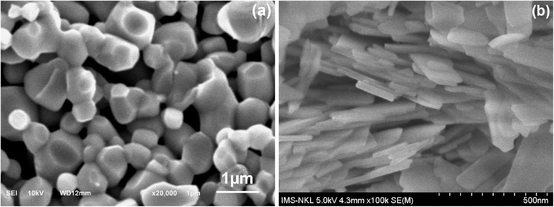 | ||
| Fig. 1 SEM images of (a) ZnO microparticles and (b) ZnO nanoplates. | ||
Fig. 1b clearly shows the plate-like morphology of ZnO nanoparticles, characterized by their thin structure, hence referred to as ZnO nanoplates. The average thickness of ZnO nanoplates is only about 15 nm and their lengths are in the range of 100–400 nm. The formation of ZnO nanoplates was explained by Sahu et al.26 as resulting from the slow addition of OH− into a Zn2+ solution. In this study, the hydrothermal process was conducted using urea at pH 5. This indicates that the initial concentration of [OH−] was very low, leading to slow reaction between Zn2+ ions with (OH−) to form Zn(OH)2 flakes. During hydrothermal process, OH− ions were generated from the thermal decomposition of urea at high temperature and in a closed reactor (CH4N2O → CO2 + NH3 → NH4OH). These Zn(OH)2 flakes were partially converted to ZnO during hydrothermal process and fully converted to ZnO after calcination, resulting in the formation of the ultra-thin ZnO nanoplate structure. The plate-like morphology of ZnO nanoparticles is a key factor in the utilization of ZnO nanoplate powder for preparing ZnO-based varistors, with the expectation of achieving excellent electrical properties.27
 | ||
| Fig. 2 (a) FTIR spectrum and (b) XRD patterns ZnO nanoplates and microparticles calcined at 600 °C for 2 h in air. | ||
Fig. 2b shows the X-ray diffraction (XRD) pattern of the ZnO nanoplates. It can be seen the diffraction peaks at 2θ positions of 31.77°, 34.42°, 36.25°, 47.53°, 56.60°, 62.86°, 66.38°, 67.98°, 69.1°, 72.58°, and 76.95°. These peaks are fitted well with the hexagonal wurtzite ZnO (JCPDS No. 00-036-1451), corresponding to its lattice planes (100), (002), (101), (102), (110), (103), (200), (112), (201), (004), and (202), respectively. This also reveals a well-defined crystalline structure of ZnO, and confirms the high purity of the ZnO phase without any secondary phase. By using eqn (1), the crystallite size value is calculated to be about 0.9 nm. Fig. 2 also shows that the FTIR and XRD spectra of micro-ZnO are quite similar to those of ZnO nanoplates.
Properties of as-synthesized nano-ZnO-based varistors
| Sample | Sintering temperature (°C) | Diametrical shrinkage (%) | Axial shrinkage (%) | Density ρ (g cm−3) | Vicker hardness (HV) |
|---|---|---|---|---|---|
| MicroZ1100 | 1100 | 17.5 ± 0.1 | 15.5 ± 0.2 | 5.49 ± 0.02 | 241 ± 2 |
| NanoZ1000 | 1000 | 17.4 ± 0.2 | 15.6 ± 0.2 | 5.52 ± 0.08 | 255 ± 4 |
| NanoZ1100 | 1100 | 17.5 ± 0.1 | 15.8 ± 0.3 | 5.56 ± 0.04 | 280 ± 5 |
| NanoZ1200 | 1200 | 17.9 ± 0.1 | 16.1 ± 0.5 | 5.38 ± 0.04 | 244 ± 4 |
The XRD patterns of both micro- and nano-ZnO-based varistor samples (Fig. 3) shows the typical composition of wurtzite ZnO (*) and Bi2O3 (Δ) phases, along with the modified spinel Zn1.82Cr0.78Sb0.41O4 or Zn(Zn0.82Cr0.78Sb0.41)O4 (#) phase. The ZnO phase, serving as the primary matrix, dominates the samples. Its three main diffraction peaks can be observed at 2θ angles of 31.78°, 34.45°, and 36.27° (±0.007°), corresponding to the lattice planes (100), (002), and (101) of the hexagonal wurtzite ZnO structure (JCPDS No. 00-036-1451). The Bi2O3 phase in cubic crystalline (JCPDS No. 01-074-1373) is also identified, with its first three peaks appearing at 22.11, 27.91 and 32.25 °C (±0.03°). Additionally, the Bi-rich tetragonal crystalline phase of Bi2O3 (γ-Bi2O3, JCPDS No. 00-018-0244) is detected in the XRD spectra of the four varistor samples, though with lower intensity.
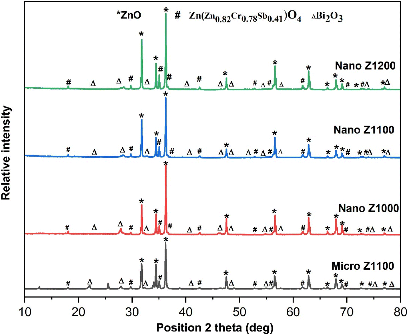 | ||
| Fig. 3 XRD patterns of ZnO based varistor ceramics sintered at 1000, 1100, and 1200 °C for 2 h. | ||
The spinel phase, Zn1.82Cr0.78Sb0.41O4 (#, Zinc Chromium Antimony Oxide, JCPDS No. 01-082-1102), becomes more prominent at higher sintering temperatures, with its characteristic peaks appearing around the 2θ angles of 18.50°, 29.76°, 35.04° (±0.01°). In this study, the molar ratio Sb2O3/Bi2O3 = 1, therefore, the spinel phase mainly forms through the decomposition from the pyrochlore phase, as reaction eqn (7). The presence of Cr2O3 prevents the formation of pyrochlore as well as the formation of conventional spinel Zn7Sb2O12, because, it can take part in the formation of modified spinel Zn1.82Cr0.78Sb0.41O4 phase, as reaction eqn (9).2,34,35 This reaction may simultaneously inhibits the formation of spinel Zn7Sb2O12 phase (reaction eqn (8)). At 1200 °C (Nano Z1200), the peak intensity of modified spinel phase increases, suggesting a complete transition from the pyrochlore phase to the new modified spinel phase (Zn1.82Cr0.78Sb0.41O4), as reaction eqn (9).35
| 3Bi2O3 (liq) + 3Sb2O3 (s) + ZnO (s) + 2O2 → 2Zn2Sb3Bi3O14 (pyrochlore) | (7) |
| 2Zn2Sb3Bi3O14 + 17ZnO → 3Zn7Sb2O12 (spinel) + 3Bi2O3 (liq) | (8) |
| Zn2Sb3Bi3O14 + 3.46ZnO + 1.17Cr2O3 → 3Zn1.82Cr0.78Sb0.41O4 + Bi2O3 + Sb2O3 + 1.485O2 | (9) |
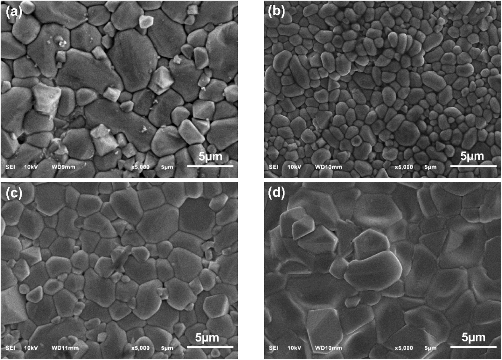 | ||
| Fig. 4 Surface SEM images of (a) MicroZ1100, (b) NanoZ1000, (c) NanoZ1100, (d) NanoZ1200 varistor. | ||
| Sample | Sintering temperature (°C) | Grain size on surface (μm) | Grain size in cross-section |
|---|---|---|---|
| NanoZ1000 | 1000 | 1.7 ± 0.2 | 1.8 ± 0.3 |
| NanoZ1100 | 1100 | 3.5 ± 0.3 | 3.8 ± 0.3 |
| NanoZ1200 | 1200 | 5.5 ± 0.6 | 6.8 ± 1.0 |
| MicroZ1100 | 1100 | 4.7 ± 0.6 | 4.8 ± 0.9 |
The SEM images of the surface of the nano-ZnO-based varistors also show the changes in the shape of ZnO grains at three sintering temperature levels. At 1000 °C, the ZnO grains appear nearly round or oval. In contrast, at sintering temperatures of 1100 °C and 1200 °C, the ZnO grains exhibit polyhedral shapes, although the raw ZnO particles initially resemble nanoplate-like structures.37 Since the initial shape of ZnO microparticles is polyhedral, the final ZnO grains are also observed as polyhedral, but with a larger size.
Fig. 5 and S3 (ESI)† displays the cross-section morphology of micro- and nano-ZnO based varistor. The summarized results in Table 2 show that the ZnO grain size also increases with sintering temperature in the varistor system that uses ZnO nanoplates as the main raw material. At the same sintering temperature of 1100 °C, the average grain size of the NanoZ1100 varistor sample is 3.3 ± 0.3 μm, significantly smaller than the average grain size of the varistor sample using micro-ZnO raw material (4.8 ± 0.9 μm). The grain size in fracture-surface of varistor samples using ZnO nanoplates also increases from 2.6 ± 0.3 μm to 6.8 ± 1.0 μm as the sintering temperature rises from 1000 to 1200 °C. Unlike the surface morphology, Fig. 5 shows that the grain boundary regions between two ZnO grains in the varistor samples can be clearly observed, especially when viewed at higher magnification (the images on the left of Fig. 5). These observations confirm the hypothesis that sintering temperature and powder type (micro vs. nano) are critical factors in microstructural evolution. In NanoZ samples, grain growth is significantly suppressed at lower temperatures due to the presence of modified spinel particles, which act as pinning agents to stabilize grain boundaries and prevent coarsening. However, at higher temperatures (1200 °C), the enhanced grain growth indicates a diminished pinning effect and increased atomic mobility, promoting grain enlargement.38
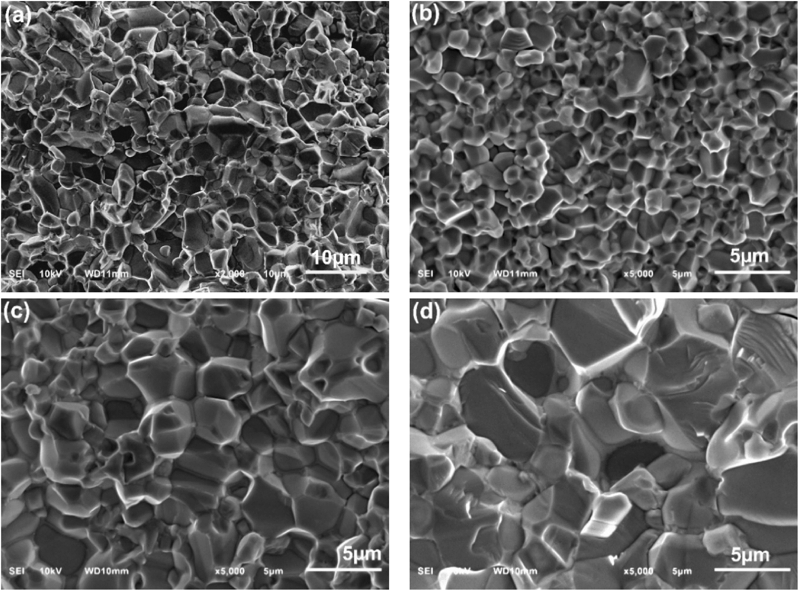 | ||
| Fig. 5 Cross-section SEM images of (a) MicroZ1100, (b) NanoZ1000, (c) NanoZ1100, (d) NanoZ1200 varistor samples. | ||
 | ||
| Fig. 6 FTIR spectra of (a) micro-ZnO-based varistor, (b) unique nano-ZnO varistor sintered at 1100 °C, and nano-ZnO-based varistors sintered at (c) 1000, (d) 1100 and (e) 1200 °C. | ||
Volt-ampere characteristic curves and DC electrical properties
Fig. 7 presents the DC volt-ampere characteristic curves, illustrating the density current (J, mA cm−2) as a function of applied electric field (E, V mm−1), along with the logarithm of DC resistivity (ρ, MΩ m) as a function of applied E. The data include micro-ZnO-based varistor sintered at 1100 °C, and nano-ZnO-based varistors sintered at 1000, 1100 and 1200 °C. The breakdown threshold (Eb, V mm−1), breakdown threshold per grain boundary (Vgb, V), nonlinear coefficient (α), and leakage current density (JL, mA cm−2) parameters determined from the E–J curves are summarized in Table 3. | ||
| Fig. 7 The voltage-ampere characteristic curves of ZnO based varistors sintered at different temperatures, (a) E–J curves; (b) E–log(resistivity) curves. | ||
| Sample | υgb (V) | E1mA (V mm−1) | α | JL (μA cm−2) |
|---|---|---|---|---|
| NanoZ1000 | 2.41 | 1336 | 34.3 | 11.9 |
| NanoZ1100 | 2.62 | 689 | 48.5 | 9.7 |
| NanoZ1200 | 1.94 | 286 | 24.6 | 27.6 |
| MicroZ1100 | 2.07 | 432 | 35.8 | 23.4 |
Fig. 7a shows that all above varistors have two distinct characteristic regions. In the first region (E < E1mA), the behavior is approximately linear behavior (α < 10) at low electric fields. In the second region (E > E1mA), the varistors demonstrate the nonlinear behavior. The nonlinear behavior of the nano-ZnO-based varistors depends on both sintering temperature and the particle size of raw ZnO material. As the sintering temperature increases, the breakdown threshold (Eb = E1mA) tends to decrease, suggesting grain growth and a reduction in the number of grain boundaries per unit length.
The nonlinearity coefficient (α) exhibits a significant variation, with the highest value observed for the sample sintered at 1100 °C (α = 48.5), indicating optimal grain boundary characteristics for nonlinear behavior. The breakdown threshold and breakdown threshold per grain boundary of NanoZ1100 (689 V mm−1, 2.62 V) are significantly higher than those of MicroZ1100 (432 V mm−1, 2.07 V). This indicates that the nano-ZnO-based varistor has a finer grain structure, resulting in more grain boundaries per unit length, which enhances the breakdown voltage.
Additionally, the leakage current density of NanoZ1100 (9.7 μA cm−2) is lower than that of MicroZ1100 (23.4 μA cm−2). This lower leakage current indicates that the grain boundaries in NanoZ1100 varistors provide more effective barrier potential, reducing undesired current flow under low-field conditions.
Fig. 7b also shows that the resistivity of the varistor samples is initially very high, around 106.5–108 Ω m, corresponding to the insulating state. As the applied electric field (E) increases, the resistivity decreases rapidly. However, a sharp drop in resistivity occurs after reaching the breakdown electric field E1mA, where the varistor transitions from a high-resistance state to a highly conductive state. In the region with E > E1mA, the resistivity decreases dramatically to around 103–104 Ω m. This sharp decline marks the transition from the pre-breakdown region to the highly conductive state, where the varistor begins to exhibit strong nonlinearity and efficient voltage clamping behavior. The resistivity behavior of the nano-ZnO varistors sintered at different temperatures (1000, 1100, and 1200 °C) shows a clear difference. The NanoZ1000 sample exhibits the highest resistivity across all electric field ranges, indicating a more insulating nature. As the sintering temperature increases to 1100 °C (NanoZ1100) and 1200 °C (NanoZ1200), the resistivity decreases, suggesting enhanced grain growth and improved electrical conductivity.
Comparing the micro-ZnO varistor (MicroZ1100) and nano-ZnO varistor (NanoZ1100), both sintered at 1100 °C, the MicroZ1100 sample shows lower resistivity than its nano counterpart at lower electric fields. However, as the electric field increases, the resistivity of NanoZ1100 decreases more rapidly, indicating a stronger nonlinearity and better varistor performance. This suggests that nano-structured ZnO enhances the breakdown characteristics and nonlinear behavior compared to micro-structured ZnO.
The results presented in Table 3 can be explained as follows. At a sintering temperature of 1000 °C, limited dopant diffusion, small ZnO grain sizes, and narrow grain boundary layers are observed. This leads in a high number of grain boundaries per unit length and a high number of depletion regions at the grain boundaries, resulting in an increase in grain boundary resistivity.40,41 However, the varistor effect, indicated by a nonlinear coefficient (α) of 34.3, remains relatively low, although a high breakdown voltage and resistivity can be achieved.
As the sintering temperature exceeds 1100 °C, ZnO grains continue to grow, forming thicker and more distinct grain boundary layers on the micrometer scale. This grain growth reduces the number of grain boundaries per unit length and decreases the resistivity of the grain boundary layer,18,19 ultimately lowering the varistor effect (α = 24.6 at a sintering temperature of 1200 °C). Similarly, when using micro-sized ZnO as the raw material, its lower specific surface area causes dopants to be distributed over a smaller area, promoting the formation of thicker grain boundary layers.
As sintering progresses at 1100 °C, ZnO grains continue to grow from the micrometer scale, further increasing grain size. Consequently, in the MicroZ1100 sample, the larger ZnO grains lead to more pronounced and thicker grain boundary layers. This results in lower overall resistance of grain boundaries compared to the NanoZ1100 sample, where the finer ZnO grains contribute to a higher density of grain boundaries and greater resistivity.
A sintering temperature of 1100 °C is considered optimal, as it balances grain boundary layer thickness and ZnO grain size while enabling efficient dopant diffusion into the grain boundary region. This ensures an improved electrical response without excessive grain growth, maintaining stable varistor performance. At this temperature, the highest nonlinear coefficient (α = 48.5) is obtained, while a moderate breakdown voltage and resistivity are still achieved.
It can be suggested that nano-ZnO-based varistors (NanoZ1100) exhibit superior electrical properties compared to micro-ZnO-based ones (MicroZ1100), including a higher breakdown field, stronger nonlinearity, and lower leakage current. Nano-ZnO particles possess a significantly higher specific surface area, which facilitates deeper dispersion of additive oxides. This results in a greater number of active sites for potential barrier formation, thereby enhancing the non-linear electrical behavior. As shown in the FESEM images, the use of nano-ZnO powders leads to varistors with fine-grained microstructures. The grains grow from the nanoscale to the microscale during sintering, resulting in smaller average grain sizes compared to those obtained using micro-ZnO powders. This finer microstructure contributes to higher breakdown voltage and improved nonlinear coefficient. These mechanisms have been observed and discussed in previous studies,36,41 and are consistent with the improved performance of our nano-ZnO-based varistors compared to those fabricated from micro-ZnO.
These advantages highlight the potential of nano-ZnO powders in enhancing varistor performance, making them more suitable for high-voltage and high-performance applications. Moreover, sintering temperature not only influences the structural properties but also impacts the nonlinear characteristics of ZnO-based varistors. Optimizing the sintering conditions at 1100 °C is essential to ensure the effective operation of varistors in power applications.
Impedance and AC electrical properties
The Cole–Cole plots of resistivity (in units of MΩ m) for ZnO-based varistors sintered at different temperatures are displayed in Fig. 8. These plots exhibit a characteristic semicircular arc, which are fitted well with the [Ro in series (Rgb//Cgb)] equivalent circuit model, as illustrated at the top of Fig. 8b.16,42 In this model, Ro represents the ohmic resistivity of ZnO, while Rgb and Cgb correspond to the grain boundary resistivity and specific capacitance, respectively.43 The AC electrical impedance properties of micro- and nano-ZnO-based varistors are summarized in Table 4. The results in Table 4 indicate that the ohmic resistivity and grain boundary resistance depend on the sintering temperature and microstructure significantly. | ||
| Fig. 8 Resistivity Cole–Cole plots of ZnO based varistors sintered at different temperatures, (a) NanoZ1000 (hollow circle); (b) NanoZ1200, (c) MicroZ1100, and (d) NanoZ1100. | ||
| Varistor sample | Ro (Ω) | ρo (Ω m) | ρ at 2 MHz (Ω m) | ρgb (MΩ m) | Rgb (MΩ) |
|---|---|---|---|---|---|
| NanoZ1000 | 1.97 | 0.083 | 11.51 | 76.90 | 1829 |
| NanoZ 1100 | 1.29 | 0.072 | 5.03 | 17.45 | 312.7 |
| NanoZ 1200 | 0.81 | 0.038 | 1.42 | 2.34 | 50.31 |
| MicroZ1100 | 1.08 | 0.049 | 2.64 | 4.55 | 100.1 |
The ohmic resistance and resistivity (Ro and ρo) show a decreasing trend as the sintering temperature increases. The highest values of Ro and ρo for the NanoZ1000 sample (1.97 Ω m and 0.083 Ω, respectively). Conversely, the lowest values of Ro and ρo for NanoZ1200 (0.038 Ω m and 0.82 Ω) suggests better electrical conductivity in the microstructure-based varistor. The moderate values of Ro (1.08–1.29 Ω) and ρo (0.049–0.072 Ω m) are observed for the Micro1100 and NanoZ1100 samples, respectively.
Grain boundary resistivity and grain boundary resistance (ρgb and Rgb) also show significant variations. The NanoZ1000 sample exhibits strong grain boundary insulation, as indicated by the largest semicircle in Fig. 8a and the highest resistivity (76.90 MΩ m), corresponding to a resistance of 1829 MΩ. As the sintering temperature increases, these values decrease significantly in the NanoZ1200 sample (ρ = 2.34 MΩ m and R = 50.31 MΩ, respectively). The MicroZ1100 and NanoZ1100 samples have a moderate grain boundary resistivity values (4.55 and 2.34 MΩ m) and resistances (100.1 and 312.7 MΩ), respectively.
In comparison within nano-ZnO-based varistor series, increasing the sintering temperature significantly reduces the grain boundary resistance (Rgb) and enhances electrical conductivity. The NanoZ1000 sample (sintered at 1000 °C) exhibits the largest semicircle, indicating the highest Rgb (1829 MΩ), which suggests strong impedance at grain boundaries. This is attributed to incomplete grain coalescence and insufficient diffusion at lower sintering temperatures. When the temperature is increased to 1100 °C (NanoZ1100), Rgb drops to 312.7 MΩ, indicating improved intergranular contact and enhanced charge transport. However, the most significant reduction is observed at 1200 °C (NanoZ1200), where Rgb decreases drastically to 50.31 MΩ, demonstrating the highest degree of grain growth and boundary connectivity among the nano-ZnO samples.
In the comparison between nano- and micro-ZnO at 1100 °C, it can be revealed the influence of grain size on electrical properties. The NanoZ1100 sample exhibits the lower Ro (0.81 Ω) and Rgb (50.31 MΩ) than MicroZ1100, indicating that grain enlargement effectively reduces intrinsic resistance. However, its grain boundary resistivity (Rgb = 4.55 MΩ·m) remains higher than that of NanoZ1200 (2.34 MΩ m), suggesting that nanoscale ZnO grains sintered at high temperatures yield superior electrical performance due to enhanced charge carrier mobility at grain boundaries. Higher sintering temperatures reduce grain boundary resistance, facilitating improved electrical conductivity. Therefore, the NanoZ1200 sample exhibits superior electrical conductivity and lower grain boundary resistance, making it suitable for low-voltage applications. In contrast, the NanoZ1100 sample, with its higher grain boundary resistance, can be applied in high-voltage applications where a higher breakdown field is required.
These findings indicate that NanoZ1000 exhibits the highest grain boundary resistance, making it suitable for applications requiring strong electrical insulation. In contrast, NanoZ1200 demonstrates the best electrical conductivity but reduced grain boundary insulation, which may be advantageous for applications requiring higher current conduction. MicroZ1100 and NanoZ1100 presents a balance between conductivity and insulation, however the MicroZ1100 sample does not outperform nano-based varistors in either aspect. These results highlight the influence of microstructure and sintering temperature on the electrical performance of ZnO-based varistors, providing insights into optimizing their applications in electronic devices.
Fig. 9 illustrates the variation of AC resistivity and the phase angle between imaginary and real part of resistivity of ZnO-based varistors as a function of frequency. The logarithmic AC resistivity curves (Fig. 9a) exhibit a decreasing trend with increasing frequency, indicating the frequency-dependent electrical behavior of the varistors. At low frequencies (f < 10 Hz), the AC resistivity values are very high (≅Rgb, 106.5–108 Ω m), and approximately equal to the DC resistivity at low applied field, due to the measurement in the nonlinear region of ZnO varistors. Among the varistor samples, NanoZ1000 exhibits the highest AC resistivity, while NanoZ1200 shows the lowest value, suggesting that the microstructure and sintering temperature significantly influence grain boundary resistance.
 | ||
| Fig. 9 (a) The AC resistivity (Ω m) and (b) the phase angle (degree) of resistivity of as a function of frequency for ZnO-based varistors. | ||
As the frequency increases (101–106 Hz), the AC resistivity of all samples converges, indicating that the contribution of grain boundary resistance diminishes, and the bulk conduction mechanism dominates. Notably, NanoZ1200 demonstrates lower resistivity compared to NanoZ1000, which aligns with the expected reduction in grain boundary resistance due to the higher sintering temperature. The phase angle plots (Fig. 9b) provide further insight into the electrical response of the varistors. At low frequencies (<1 Hz), the phase angle is close to 0°, indicating predominantly resistive behavior. As the frequency increases, the phase angle rapidly shifts towards −90°, signifying a transition from resistive to capacitive characteristics. This shift occurs more abruptly for NanoZ1000 and NanoZ1100, suggesting stronger grain boundary effects and polarization phenomena compared to NanoZ1200 and MicroZ1100.
Conclusions
This work explores the effects of sintering temperatures on the structural, mechanical, and electrical properties of nano-ZnO varistors. By optimizing the sintering process and utilizing the appropriate dopant oxide system, significant improvements in microstructural uniformity and electrical performance have been achieved successfully for nano-ZnO varistors. Once sintered at temperatures of 1000–1200 °C, the values of their shrinkage, average grain size and hardness are 17–19%, 1.7–6.8 μm, and 200–280 HV, respectively. At the optimal sintering temperature (1100 °C), the nano-ZnO varistors achieved a balance between high nonlinearity (α = 48.5), low leakage current (JL = 9.7 μA cm−2), and relatively high breakdown field (E = 689 V mm−1). For all samples, the values of grain boundary electrical resistivity at low frequency were similar to those of DC resistivity at the low applied electric fields (∼106.5–108 Ω m). However, at the higher frequencies, the values of AC resistivity and phase angle showed a characteristic transition from resistive to capacitive behaviors, with a more pronounced shift for NanoZ1000 and NanoZ1100 samples. These findings might provide a fundamental understanding of the structure–property relationship in ZnO varistors, which can be further optimized for specific industrial applications.Data availability
The data available within the article and its ESI.†Author contributions
Tham Do Quang: conceptualization (lead), formal analysis (equal); funding acquisition (lead); investigation (equal); methodology (equal); visualization (equal); writing – original draft (equal), review and editing (lead). Huy Nguyen Trung: methodology (equal); visualization (equal); investigation (equal), writing – original draft (lead). Trang Nguyen Van, Kieu Anh Vo Thi, Hong Cao Thi, Xuyen Nguyen Thi, Tuan Anh Nguyen (Bsc), Chinh Tran Van, Duy Lai Van: formal analysis (equal), investigation (equal); methodology (equal); visualization (equal), writing – original draft (equal). Tuan Anh Nguyen (Dr), Lam Tran Dai: review (equal). Duong Duc La: original draft, review and editing (equal).Conflicts of interest
The authors declare no competing interests.Acknowledgements
This research is funded by Ministry of Science and Technology (MOST) of Vietnam under grant number ĐTĐLCN.22/23.References
- T. Tian, L. Zheng, M. Podlogar, H. Zeng, S. Bernik and K. Xu, et al., Novel ultrahigh-performance ZnO-based varistor ceramics, ACS Appl. Mater. Interfaces, 2021, 13(30), 35924 CrossRef CAS PubMed.
- M. Kelleher, Chapters 34: ZnO varistors – the ideal microstructure and characteristics, and methods investigated and developed to achieve these, Encyclopaedia of Materials: Electronics, Academic Press, 2023. vol. 3, pp. 392–418 Search PubMed.
- J. He, Metal Oxide Varistors: from Microstructure to Macro-Characteristics, John Wiley & Sons, Germany, 2019 Search PubMed.
- H. Lu, Y. Wang and X. Lin, Structures, varistor properties, and electrical stability of ZnO thin films, Mater. Lett., 2009, 63(27), 2321 CrossRef CAS.
- S. C. Pillai, J. M. Kelly, R. Ramesh and D. E. McCormack, Advances in the synthesis of ZnO nanomaterials for varistor devices, J. Mater. Chem. C, 2013, 1(20), 3268 RSC.
- N. Daneu, G. N. Novak, A. Rečnik, M. Maček Kržmanc and S. Bernik, Shock-sintering of low-voltage ZnO-based varistor ceramics with Bi4Ti3O12 additions, J. Eur. Ceram. Soc., 2013, 33(2), 335 CrossRef CAS.
- D. R. Clarke, Varistor Ceramics, J. Am. Ceram. Soc., 1999, 82(3), 485–502 CrossRef CAS.
- P. Roy, Synthesis of nano ZnO powder and study of its varistor behavior at different temperatures, J. Mater. Sci. Res., 2012, 1(4), 28–34 CAS.
- Y. Q. Huang, L. Meidong, Z. Yike, L. Churong, X. Donglin and L. Shaobo, Preparation and properties of ZnO-based ceramic films for low-voltage varistors by novel sol-gel process, Mater. Sci. Eng. B, 2001, 86(3), 232–236 Search PubMed.
- M.-H. Wang, C. Yao and N.-F. Zhang, Degradation characteristics of low-voltage ZnO varistor manufactured by chemical coprecipitation processing, J. Mater. Process. Technol., 2008, 202(1), 406 CrossRef CAS.
- S. Anas, K. V. Mahesh, M. Jeen Maria and S. Ananthakumar, Sol-gel materials for varistor devices, in Sol-gel Materials for Energy, Environment and Electronic Applications, ed. Pillai S. C. and Hehir S., Springer International Publishing, New York, 2017, pp. 23–59 Search PubMed.
- R. Zamiri, B. K. Singh, D. Dutta, A. Reblo and J. M. F. Ferreira, Electrical properties of Ag-doped ZnO nano-plates synthesized via wet chemical precipitation method, Ceram. Int., 2014, 40(3), 4471 CrossRef CAS.
- S. Boily, H. Alamdari, G. Cross, A. Joly, A. Van Neste and P. Grütter, et al., Ball milled ZnO for varistor applications, Mater. Sci. Forum, 1996, 235–238, 993 Search PubMed.
- J. Zhu, G. Qi, L. Wang, H. Yang and F. Wang, Influence of intensive milling on the microstructure and electrical properties of ZnO–Bi2O3-based varistors, Ceram. Int., 2012, 38, S463 Search PubMed.
- Z. Li, X. Ren, X. Wang, W. You, M. Zhong and A. Kong, et al., Effectively enhanced comprehensive electrical performance of ZnO varistors by a fast combinatorial refinement method, Mater. Sci. Semicond. Process., 2021, 133, 105945 CrossRef CAS.
- A. Boumezoued, K. Guergouri, R. Barille, R. Djamil and Z. Mourad, Synthesis and characterization of ZnO-based nano-powders: study of the effect of sintering temperature on the performance of ZnO–Bi2O3 varistors, J. Mater. Sci.: Mater. Electron., 2021, 32, 1–15 Search PubMed.
- S. Anas, P. Mukundan, A. M. Sanoj, V. R. Mangalaraja and S. Ananthakumar, Synthesis of ZnO based nanopowders via a non-hydrolytic sol gel technique and their densification behaviour and varistor properties, Process. Appl. Ceram., 2010, 4, 7–14 CrossRef CAS.
- S. C. Pillai, J. M. Kelly, D. E. McCormack and R. Ramesh, High performance ZnO varistors prepared from nanocrystalline precursors for miniaturised electronic devices, J. Mater. Chem., 2008, 18, 3926 RSC.
- W. Liu, L. Zhang, F. Kong, K. Wu, S. Li and J. Li, Enhanced voltage gradient and energy absorption capability in ZnO varistor ceramics by using nano-sized ZnO powders, J. Alloys Compd., 2020, 828, 154252 CrossRef CAS.
- L. Van Duy, T. T. Nguyet, C. M. Hung, D. T. Thanh Le, N. Van Duy and N. D. Hoa, et al., Ultrasensitive NO2 gas sensing performance of two dimensional ZnO nanomaterials: Nanosheets and nanoplates, Ceram. Int., 2021, 47(20), 28811 Search PubMed.
- S. Farhat, M. Rekaby and R. Awad, Vickers microhardness and indentation creep studies for erbium-doped ZnO nanoparticles, SN Appl. Sci., 2019, 1(6), 546 CrossRef CAS.
- M. A. Ashraf, A. H. Bhuiyan, M. A. Hakim and M. T. Hossain, Microstructure and electrical properties of Ho2O3 doped Bi2O3-based ZnO varistor ceramics, Phys. B, 2010, 405(17), 3770 CrossRef CAS.
- M. T. Islam, A. Dominguez, B. Alvarado-Tenorio, R. A. Bernal, M. O. Montes and J. C. Noveron, Sucrose-mediated fast synthesis of zinc oxide nanoparticles for the photocatalytic degradation of organic pollutants in water, ACS Omega, 2019, 4(4), 6560 Search PubMed.
- ASTM, D257-14: Standard test methods for DC resistance or conductance of insulating materials, 2014.
- M. Lisowski and K. Ryszard, Changes proposed for the IEC 60093 standard concerning measurements of the volume and surface resistivities of electrical insulating materials, IEEE Trans. Dielectr. Electr. Insul., 2006, 13(1), 139 CrossRef.
- K. Sahu, S. kuriakose, J. Singh, B. Satpati and S. Mohapatra, Facile synthesis of ZnO nanoplates and nanoparticle aggregates for highly efficient photocatalytic degradation of organic dyes, J. Phys. Chem. Solids, 2018, 121, 186 CrossRef CAS.
- C. M. Hung, L. Van Duy, D. T. Thanh Le, H. Nguyen, N. Van Duy and N. D. Hoa, ZnO coral-like nanoplates decorated with Pd nanoparticles for enhanced VOC gas sensing, J. Sci. Adv. Mater. Devices, 2021, 6(3), 453 CrossRef CAS.
- G. B. Karki, K. Parajuli, S. Adhikari, S. P. Khatiwada and R. Adhikari, Facile synthesis of zinc carbonate and zinc oxide nanoparticles and their antimicrobial properties, J. Nepal Biotech. Assoc., 2023, 4(1), 37 CrossRef.
- K. R. S. Murthy, G. K. Raghu and P. Binnal, Zinc oxide nanostructured material for sensor application, J. Adv. Biotechnol. Bioeng., 2021, 5(1), 25 Search PubMed.
- S. D. Birajdar, R. C. Alange, S. D. More, V. D. Murumkar and K. M. Jadhav, Sol-gel auto combustion synthesis, structural and magnetic properties of Mn doped ZnO nanoparticles, Procedia Manuf., 2018, 20, 174 CrossRef.
- A. Karim, Effect of Compaction Parameters and Sintering Configurations on the Performance of ZnO Varistor, Dublin City University, 1996 Search PubMed.
- N. Riahi-Noori, Comparison of electrical properties of zinc oxide varistors manufactured from micro and nano ZnO powder, J. Ceram. Process. Res., 2011, 12, 752∼5 Search PubMed.
- L. S. Macary, M. L. Kahn, C. Estournès, P. Fau, D. Trémouilles and M. Bafleur, et al., Size effect on properties of varistors made from zinc oxide nanoparticles through low temperature spark plasma sintering, Adv. Funct. Mater., 2009, 19(11), 1775–1783 Search PubMed.
- Y. Zheng, M. Fujimoto, Y. Sato and S. Yoshikado, Effects of addition of chromium and/or nickel oxides on the electrical characteristics of yttrium oxide-doped high-voltage zinc oxide varistors, J. Eur. Ceram. Soc., 2021, 41(9), 4841–4849 CrossRef CAS.
- N. T. Hung, N. D. Quang and S. Bernik, Electrical and microstructural characteristics of ZnO–Bi2O3-based varistors doped with rare-earth oxides, J. Mater. Res., 2001, 16(10), 2817–2823 CrossRef CAS.
- L. Tang, D. Zhao, X. Chi, W. Chen, S. Hu and G. Wang, Research Progress of ZnO Nonlinear Varistor Grain Boundary Microstructure, Insul. Surge Arresters, 2021, 03(301), 162–178 Search PubMed.
- B.-H. Chen, B.-W. Wang, P.-Z. Gao, P. Zhang and H.-H. Chen, Effects of raw particle size and annealing on microstructure, electrical and mechanical behaviors of ZnO-based varistors, J. Alloys Compd., 2021, 872, 159638 CrossRef CAS.
- D. Q. Tan, Superior performing nano-enabled metal oxide varistors, Int. J. Ceram. Eng. Sci., 2019, 1(3), 136–143 Search PubMed.
- M. S. Tanweer, Z. Iqbal, A. M. Rather and M. Alam, Zinc oxide/moringa oleifera gum-grafted L-methionine-functionalized polyaniline bionanocomposites for water purification, Water, 2024, 16(18), w16182576 CrossRef.
- A. Bouchekhlal and M. Boulesbaa, Synthesis and characterization of ZnO based varistor ceramics: effect of sintering temperatures, Microelectron. Int., 2022, 39(3), 110–120 CrossRef.
- Y. Kajikawa, Effects of potential barrier height and its fluctuations at grain boundaries on thermoelectric properties of polycrystalline semiconductors, J. Appl. Phys., 2013, 114(5), 053707 Search PubMed.
- J. Porcayo-Calderon, J. J. Ramos-Hernandez, C. D. Arrieta-Gonzalez, J. G. Chacon-Nava, J. G. Gonzalez-Rodriguez and E. Porcayo-Palafox, et al., Synthesis by hydrothermal treatment of ZnO-based varistors doped with rare earth oxides and their characterization by impedance spectroscopy, Crystals, 2020, 10(12), 1134 Search PubMed.
- W. Lin, Z. Xu, Z. Wang, J. Yang, C. Zhu and R. Chu, Influence of Bi3Zn2Sb3O14 pre-synthesis phase on electrical properties of the ZnO-Bi2O3 based varistor ceramics, J. Alloys Compd., 2020, 834, 155070 CrossRef CAS.
Footnote |
| † Electronic supplementary information (ESI) available. See DOI: https://doi.org/10.1039/d5ra01534k |
| This journal is © The Royal Society of Chemistry 2025 |