DOI:
10.1039/D5RA01415H
(Paper)
RSC Adv., 2025,
15, 18456-18466
Rational design of a lead-free Cs2Na0.4Ag0.6In0.9Bi0.1Cl6:0.15Mn2+ double perovskite for enhancing the colour rendition index of UV-pumped W-LEDs†
Received
27th February 2025
, Accepted 20th May 2025
First published on 3rd June 2025
Abstract
Compared with lead halide perovskites, double perovskites (DPs) have drawn much attention because of their intriguing optoelectronic qualities, environmental stability, and non-toxicity. Herein, we systematically designed a Cs2Na0.4Ag0.6In0.9Bi0.1Cl6:0.15Mn2+ double perovskite by alloying Ag+ and Bi3+ at the Na+ and In3+ sites in the host lattice. Ag+ broke the parity forbidden transition of Cs2NaInCl6, and Bi3+ significantly broadened the emission spectra from 450–700 nm. Doping of Mn2+ further reduced the defect density and enhanced the radiative recombination. Broad emission owing to the 4T1 → 6A1 transition of Mn2+ ions was observed at 665 nm. Upon doping, the sample exhibited a PLQY of 44.9%. Temperature-dependent emission characteristics of the synthesized double perovskite were also studied. Even at a high temperature of 100 °C, the emission intensity was reduced only by 53%, and the material possessed a high activation energy of 0.46 eV. The optimised sample was physically blended with blue emitting BaMgAl10O17:Eu2+ to obtain complete spectral color coverage in visible light when excited with a 365 nm UV light source. CIE coordinates of (0.37, 0.39), CCT of 4457.53 K and CRI of 87.4 were obtained for the optimised sample. Cs2Na0.4Ag0.6In0.9Bi0.1Cl6:0.15Mn2+ was found to be a promising luminescent material for enhancing the color rendition index of UV-pumped white LEDs. The as-prepared double perovskite is a multifunctional material that can be used for WLEDs, photodetectors and display screens.
1. Introduction
Perovskite materials are gaining importance in optoelectronic applications, such as light emitting diodes, solar cells, photo-detectors, scintillators and lasers, owing to their tunable band gap, high light absorption ability, low defect density, high carrier mobility and large charge diffusion lengths.1–5 White light can be obtained using any of the following three methods: combining tri-color emitting (red, green and blue) LEDs, using UV-LEDs in combination with red-, blue- and green-emitting phosphors and utilising phosphor-converted LEDs. Owing to the high energy efficiency and low spectral mismatch of phosphor-converted LEDs, they are more commonly utilized for commercial purposes.6 Phosphor-converted LEDs use the combination of an InGaN blue LED chip with a YAG:Ce3+ yellow emitting phosphor or an inorganic phosphor, such as (SrMg2La2W2O12:Mn4+),7 (Ca2YSbO6:Eu3+),8 (Sr3La(BO3)3:Ce, Tb),9 (NaBaY(BO3)2:Ce3+, Tb3+),10 and (NaZnPO4:Mn).11 However, phosphor-converted LEDs have some drawbacks, such as high cost owing to the involvement of rare earth dopants and color shift due to the potential degradation of phosphor over time. A major drawback of WLEDs is the low color rendition index because the overall emission spectrum lacks a red light component.12–14
The low CRI is due to the inadequate amount of the red component. CRI is defined as the scale that is used to compare the rendering of natural colors of any object in artificial white light with that of sunlight. The lower CRI with a huge CCT may cause defects in the human retina owing to the versatile emission of blue light from the semiconductor chip. Poor CRI also affects the circadian rhythm, alertness, and cognitive performance of an individual.15 Pc-LEDs also suffer from Stokes shift energy loss, narrow emission bands and phosphor degradation. To overcome the shortcomings of Pc-converted LEDs, novel materials have been explored, such as carbon quantum dots,16 lead halide perovskites,17 and metal–organic framework-based materials.18,19 Lead halide perovskites possess unique optical and electronic properties; however, owing to the inherent toxicity of lead, lead halide perovskite nanocrystals (NCs),3–5 such as (CsZnxPb1−xX3 NCs),17 ((C6H5C2H4NH3)2PbCl2Br2),20 and (CsPb(Br0.4, I0.6)3),21 are used in LEDs. The toxicity of lead halide perovskites owing to the presence of lead limits their practical applications. Tin-based perovskite material ASnX3 suffers from poor stability at room temperature owing to the unstable nature of (Sn2+).22–24 Lead free inorganic halide double perovskites A2B(I) B(III)X6 (A = Rb+ and Cs+; B(I) = K+, Na+, Ag+, and Li+; B(III) = Bi3+, In3+, and Sb3+; X = Br, I, and Cl) are non-toxic alternatives to lead- and tin-based halide perovskites. However, these emerging double perovskites face challenges, such as an indirect band gap and low photoluminescence quantum yield (<3%), owing to their parity-forbidden transitions. Cs2NaInCl6 is a potential direct band gap candidate that exhibits photo luminescence owing to self-trapped excitons, resulting in parity-forbidden transitions. To improve the photoluminescence quantum yield, various strategies, such as doping and alloying, are employed.23,25,26 Luminescence from Cs2NaInCl6 arises owing to self-trapped excitons arising from the Jahn–Teller distortion of the NaCl6 octahedron, which causes parity-forbidden transitions to be seldom allowed.
Motivated by the same, we investigate the role of alloying Ag+ and Bi3+ at Na+ and In3+ sites in the Cs2NaInCl6 lattice, respectively. Further, Mn2+ ions are used as dopants to enhance the emission in the orange-red region of the visible spectra. Optimised sample Cs2Na0.6Ag0.4In0.9Bi0.1Cl6:0.15Mn2+ was found to exhibit broadband spectra (410–800 nm) with a quantum efficiency of 44.9%. The structural and morphological properties of the DPs were explored using X-ray diffraction (XRD), Raman spectra, Field Emission Scanning Electron Microscope (FE-SEM) and High-Resolution Transmission Electron Microscope (HR-TEM). It is important to ensure the thermal stability of the luminous material to ensure that the light output from the LEDs remains reliable over an extended time. The thermal stability of the sample was tested; it was found that the emission intensity of the sample stayed up to ∼45% of its original value even at a high temperature of 100 °C. A composite of the DP sample was prepared with a blue emitting phosphor of BaMgAl10O17:Eu2+ (BAM) to obtain a broad emission in the visible spectra under UV excitation (350 nm). Various samples with varying concentrations of BAM: DP perovskite powder were prepared and spectral parameters, such as CIE coordinates, color purity, CRI and CCT, were calculated.
2. Experimental procedure
2.1. Materials and methods
Cesium chloride (CsCl, 99.9%), sodium chloride (NaCl, 99.9%), indium(III) chloride (InCl3, 99.9%), bismuth(III) acetate (CH3COOBi, 99.9%), manganese(II) chloride (MnCl2) and silver(I) acetate (CH3COOAg, 99.9%) were purchased from Sigma Aldrich and were used without any further purification.
To synthesize Cs2Na0.6Ag0.4In0.9Bi0.1Cl6:0.15Mn2+, 2 mmol of NaCl, 2 mmol of InCl3, 0.8 mmol of AgCl, 0.4 mmol of BiCl3 and 0.15 mmol of MnCl2 were dissolved in a beaker with 20 ml of HCl. The reaction temperature was kept constant at 80 °C throughout the reaction. After the precursor materials were dissolved completely in HCl, a 4 mmol solution of CsCl was added to the clear solution under constant stirring, and a white precipitate was formed. For an hour, the reaction was allowed to stir. The reaction mixture was centrifuged, and the obtained filtrate was then stored in a hot air oven for 8 hours at 60 °C for drying. The schematic representation of the synthesis procedure is shown in Scheme 1. The brief procedure for the preparation of the Cs2NaInCl6 sample is described in the ESI file in Section 2.†
 |
| | Scheme 1 Schematic of the various steps involved in the synthesis of Cs2Na0.6Ag0.4In0.9Bi0.1Cl6:0.15Mn2+ perovskite. | |
2.2. Preparation of a composite of Cs2Na0.4Ag0.6In0.9Bi0.1Cl6:0.15Mn2+ with BaMgAl10O17:Eu2+
The optimised sample of Cs2Na0.4Ag0.6In0.9Bi0.1Cl6:0.15Mn2+ microcrystals was made into a fine powder using a motor and pestle. It was physically blended with the as-prepared blue emitting phosphor BaMgAl10O17:Eu2+ (BAM:Eu2+) using isopropyl alcohol as a solvent. After physical blending, the composite samples were allowed to dry at room temperature. BAM:Eu was prepared via a solid-state reaction process, which is explained in Section 1 in the ESI file.† The prepared DPs Cs2Na0.4Ag0.6In0.9Bi0.1Cl6:0.15Mn2+ were mixed with different ratios of as-synthesized BAM:Eu. The ratios are listed in Table 3. Photoluminescence spectroscopy was recorded for all the composite samples, and various spectral parameters, such as CRI, CIE and CCT, were calculated. The synthesis of BAM:Eu2+ phosphor is described in Section 1 of the ESI file.†
2.3. Characterization tools
A Bruker D8 ADVANCE device fitted with a Cu Kα (0.1541 nm) radiation source was used to capture the powder XRD patterns of the prepared perovskite material. The elemental composition of the prepared DPs is analysed through Raman Spectroscopy (Horiba France, XploRA PLUS). Morphological and elemental analyses are performed using a field emission-scanning electron microscope equipped with EDS (FE-SEM, Thermo Fisher, FEI QUANTA 250 FEG). A high-resolution transmission electron microscope (HR-TEM, FEI–TECNAI, G2-20 TWIN, Operating voltage: 200 kV) is used to calculate the average particle size of the prepared DPs. Thermal gravimetric analysis (TGA) helps to determine the thermal stability of the DP material. The optical properties of the prepared samples were characterised using an Agilent UV-vis-NIR spectrophotometer. Steady state and time-resolved photoluminescence spectroscopy at room temperature were performed using photoluminescence spectroscopy (Edinburgh Instruments UK, FLS1000-SS-s). Temperature-dependent photoluminescence spectra for the prepared DPs were recorded using FLMS15147.
2.4. Colorimetric theory
The color of any emitting material can be defined using Commission Internationale de l'Eclairage (CIE) coordinates. The CIE coordinates for ideal white light are x = 0.33 and y = 0.33. Color Correlation Temperature (CCT), CRI, LE and lifespan are also important spectral parameters that are used to evaluate artificial lightning.27
2.4.1. CCT. By evaluating the tested light source's chromaticity against the ideal blackbody radiators, the Color Correlated Temperature (CCT) allows one to specify the appearance of light. A heated blackbody radiator's spectral component at this temperature expressed in Kelvin (K) is matched by the color of a tested light source of a particular CCT. Different emotions can be evoked by lighting sources with varying CCT values. The light turns into cool white light when its CCT exceeds 5000 K. Warm white light is approximately 2700 K, while neutral white light is approximately 4000 K.27 It can be calculated using the following McCamy equation:
| CCT = −449n3 + 3535n2 − 6823.3n + 5520.33, |
where n = (x − xe)/(y − ye) is the inverse slope line and (xe = 0.3320, ye = 0.1858) is the “epicenter”.
2.4.2. CRI. The Color-Rendering Index (CRI) is a crucial parameter that represents the ability of a light source to render the colors of various physical objects faithfully compared to natural sunlight or a standard light source. CRI is a quantitative parameter that is measured on a scale of 0–100. A CRI value of 100 shows that the color of the object appears to be the same as that under sunlight. Light sources with a CRI (<80) are usually not acceptable for indoor lighting.28,29 When eight CIE standard color samples are exposed to a light source and a reference illuminant of the same CCT, the chromaticity differences are used to calculate the CRI according to CIE 3.31995 (ref. 27).
ΔEuvw represents the mean color difference, i.e. the separation between two colors on CIE color space.
2.4.3. CIE. The color of any light source, which can be reflecting or self-luminous, can be described using Commission International de L'Eclairage (CIE) chromaticity coordinates. CIE coordinates make it convenient to specify the color of any light source. CIE 1931 colour space is a gamut of all physiologically perceived colors.30 The CIE system defines colors in terms of parameter Y and two color coordinates x and y that represent the measurement of luminance. [X], [Y] and [Z] are the vector components that refer to three-dimensional spaces, which are used as a geometric expression of colors and are also called color space. Spectral power at each wavelength with the weighting factor from the three color matching functions is denoted. The summing up of [X], [Y] and [Z] provides tristimulus values from which CIE coordinates x and y are calculated. Tristimulus values X, Y, and Z denote the amounts of primary colors required to match the required colors, where X and Y correspond to red and green, respectively, and Z corresponds to blue.31–33 From [X, Y, Z], the (x, y, z) color chromaticity co-ordinates are calculated as follows:
3. Results and discussion
3.1. Structural property
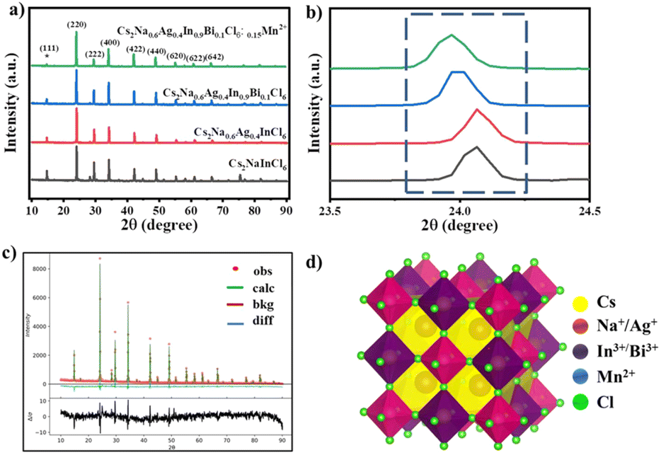
3.1.1. X-Ray diffraction spectroscopy. To analyse the crystallographic structure of the as-synthesised double perovskite material powder, XRD studies were carried out. Mn2+ ions are used as a dopant, and their concentration was kept constant at 0.15 mmol. Cs2NaInCl6 lattice was alloyed with silver and bismuth to obtain a series of samples of Cs2Na1−xAgxIn1−yBiyCl6:Mn2+ (where x = 0, 0.2, 0.4, 0.6, 0.8, and 1 and y = 0.1, 0.3, 0.5, 0.7, and 1), as shown in Fig. S3(a) and (b).† In our studies, we found out that alloying of Ag+ resulted in lattice expansion, and Bi3+ resulted in lattice contraction owing to their larger ionic radius compared to Na+ and In3+, respectively. As per the powder XRD pattern, alloying of Ag+ at the Na site does not result in any shift in diffraction peaks because of similar ionic radii of Ag+ (1.15 Å) and Na+ (1.02 Å). Here, the concentration of Ag+ (x = 0.2, 0.4, 0.5 and 0.6 mmol) increases, and there is a gradual decrease in the plane position (111), which corresponds to the 2θ of ∼14.58° due to the interference of Ag+.12 The addition of Bi3+ (1.03 Å), which has considerably larger ionic radii than In3+ (0.94 Å), might have caused lattice contraction, resulting in a shift in the peaks towards a lower angle from 24.19° to 23.99°. Alloying Bi3+ was found to cause a significant shift of 0.07° in the (220) diffraction peak towards the lower angle side. These results show the successful incorporation of both Ag+ and Bi3+ ions into the perovskite structure.3 Doping of Mn2+ slightly alters the crystal structure of the prepared double perovskite material and the slight shift towards a lower angle in the peak position ranging from 23.99° to 23.96°.34 Doping of Mn2+ causes a slight shift from 0.03° to the lower angle. Fig. 1(a) depicts the powder XRD pattern of Cs2NaInCl6, Cs2Na0.4Ag0.6InCl6, Cs2Na0.4Ag0.6In0.9Bi0.1Cl6 and Cs2Na0.4Ag0.6In0.9Bi0.1Cl6:0.15Mn2+ samples. Fig. 1(b) illustrates the enlarged view of the (220) peak to show the shifting in the diffraction peak. Fig. 1(c) and (d) depict the refinement of the pristine structure carried out by GSAS-II software and the crystal structure of the synthesised perovskite materials, respectively. This clearly shows that both double perovskite materials Cs2NaInCl6 and Cs2AgInCl6 consist of the same high-symmetry face-centered cubic structure with the space group of Fm![[3 with combining macron]](https://www.rsc.org/images/entities/char_0033_0304.gif) m, with which the [AgCl6]/[NaCl6] octahedra are attached alternatively to [InCl6] to form a 3D structure.35
m, with which the [AgCl6]/[NaCl6] octahedra are attached alternatively to [InCl6] to form a 3D structure.35
 |
| | Fig. 1 (a) Powder XRD of Cs2NaInCl6, Cs2Na0.6Ag0.4InCl6, Cs2Na0.6Ag0.4In0.9Bi0.1Cl6 and Cs2Na0.6Ag0.4In0.9Bi0.1Cl6:0.15Mn2+. (b) Shift in the peak position of the (220) plane. (c) Refinement of Cs2NaInCl6. (d) Crystal structure of pristine perovskite. | |
Further, the calculation of the average grain size and the lattice strain of the double perovskites is carried out with the WH plot using the following formula:
where
ε denotes lattice strain,
λ denotes the wavelength of X-ray (
i.e. Cu Kα = 1.5406 Å),
β denotes the full width half maxima and
D denotes the crystalline size. The WH plots are illustrated in Fig. S4.
† The strain and the crystalline size are illustrated in
Table 1.
Table 1 Crystalline size, strain, dislocation density and lattice parameter (a = b = c) of samples calculated using powder XRD data
| Sample |
Crystallite size (nm) |
Strain |
Dislocation density (m−2) |
Lattice parameter (Å) (a = b = c) |
| Cs2NaInCl6 |
132 |
1.1 × 10⁻³ |
0.63 |
10.51 |
| Cs2Na0.6Ag0.4InCl6 |
171 |
1.5 × 10⁻³ |
0.59 |
10.52 |
| Cs2Na0.6Ag0.4In0.9Bi0.1Cl6 |
65 |
1.7 × 10⁻⁴ |
0.53 |
10.48 |
| Cs2Na0.6Ag0.4In0.9Bi0.1Cl6:0.15Mn2+ |
114 |
1.3 × 10⁻³ |
0.43 |
10.47 |
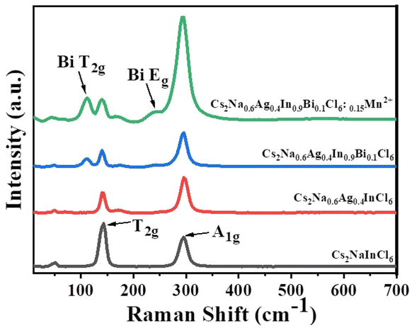
3.1.2. Raman spectroscopy. To attain clear information about the vibrational modes to understand the structure and composition, the samples were subjected to Raman vibrational spectroscopy using a 532 nm laser, as shown in Fig. 2. Two major peaks were observed for the pristine structure of Cs2NaInCl6, and they were located at 139.4 and 290.5 cm−1, corresponding to the peak positions of T2g and A1g, respectively.36 Peaks at 139.4 and 290.5 cm−1 are due to the bending (T2g) and stretching (A1g) of [InCl6]3− octahedron in Cs2NaInCl6, respectively.37 Upon incorporation of Ag, T2g peak intensity was found to be reduced, and A1g intensity increased due to the asymmetric stretching vibration of [AgCl6]5− octahedron.38,39 When a fixed amount of Bi3+ was included in the lattice, two new vibrational peaks were noticed: a peak at 111.1 cm−1, indicating the T2g peak, and another at 236.8 cm−1, denoting the Eg peak.40,41 Upon incorporation of Mn as a dopant, the intensity of A1g was found to increase, and no shift was observed owing to the minimal percentage of doping.42
 |
| | Fig. 2 Raman spectra of Cs2NaInCl6, Cs2Na0.6Ag0.4InCl6, Cs2Na0.6Ag0.4In0.9Bi0.1Cl6 and Cs2Na0.6Ag0.4In0.9Bi0.1Cl6:0.15Mn2+. | |
3.2. Morphological property
3.2.1. Scanning electron microscopy. The SEM images and the EDS mapping of the optimized amount of Ag+ and Bi3+ (Cs2Na0.4Ag0.6In0.9Bi0.1Cl6:0.15Mn2+) are further taken for the morphological analysis, as shown in Fig. 3(a–d). Fig. 4(e) shows the elemental mapping of the optimised sample. The SEM image reveals that the synthesised materials are face-centred crystals with an octahedral geometry.34,40 Fig. 3(f) shows the EDS analysis that confirms the presence of Cs, Na, Ag, In, Bi, Cl and Mn elements; no spurious peaks were observed.
 |
| | Fig. 3 (a–d) FE-SEM image of Cs2Na0.6Ag0.4In0.9Bi0.1Cl6:0.15Mn2+, (e) elemental mapping and (f) EDS mapping of Cs2Na0.6Ag0.4In0.9Bi0.1Cl6:0.15Mn2+. | |
 |
| | Fig. 4 (a) HR-TEM image (inset: particle size distribution), (b) d-spacing and (c) SAED pattern of Cs2Na0.6Ag0.4In0.9Bi0.1Cl6:0.15Mn2+. | |
3.2.2. Transmission electron microscopy. The high-resolution TEM images are shown in Fig. 4(a). The average particle size of the optimised double perovskite material Cs2Na0.6Ag0.4In0.9Bi0.1Cl6:0.15Mn2+ was calculated to be ∼32.85 ± 1.19 nm. Particles found to be irregular in shape (Fig. 4(b)) denote the images captured at a high magnification of 50k×, indicating the Moire fringes with a spacing of 0.3350 nm, which matches the d-spacing of the (222) plane. Fig. 4(c) illustrates the selective area electron diffraction pattern (SAED) of Cs2Na0.6Ag0.4In0.9Bi0.1Cl6:0.15Mn2+, which indicates that the as-prepared perovskite material is highly crystalline. The d-spacings calculated from these rings are 0.372, 0.2659, and 0.2342 nm, corresponding to the (220) (400), and (420) planes, respectively, compared with the powder-XRD results.
3.2.3. X-Ray photoelectron spectroscopy. X-Ray Photoelectron Spectroscopy is a surface-sensitive tool that can be used to determine the bonding of elements in mixed halide perovskites. The entire survey spectra of Cs2NaInCl6 and Cs2Na0.6Ag0.4In0.9Bi0.1Cl6:0.15Mn2+ are shown in Fig. 5(a) and (b). The presence of Cs, Na, In, Cl, Ag, Bi, and Mn is evident in the perovskite. The high-resolution core spectra of Cs, Na, In, Cl, Ag, Bi, and Mn are shown in Fig. 5(c–i). After deconvolution, the high-resolution spectra were fitted with the Gaussian function.43 The existence of Cs 3d photoelectrons shows that the binding energies at 726 and 739 eV correspond to the 3d3/2 and 3d5/2 spin-orbital states, respectively. The core level spectra for Na 2s and Na 1s show the binding energy peaks at 1066 and 1073 eV, respectively. The peaks at 447 and 445 eV indicate In 3d5/2 and 3d3/2, respectively. The core level spectrum of Cl 2p has a vibrant peak at a binding energy of 200 eV, which is assigned to be the 2p3/2 spin state, and a less intense peak is noticed at a binding energy of 200 eV, which is assigned to be the 2p1/2 state.44,45 The binding energies obtained at 370 and 376 eV indicate the presence of Ag 3d5/2 and Ag 3d3/2, respectively.38,40 The peaks at 161 and 164 eV correspond to the binding energies of Bi 4f5/2 and Bi 4f7/2, respectively.46 The Mn 2p binding energies are obtained at peak positions of 643 and 655 eV, which correspond to the 2p3/2 and 2p1/2, respectively. At higher energies, a satellite peak that excites the Mn 2p3/2 level is associated with the inelastic scattering of a photoelectron with a valence electron. Consequently, Fig. 6(f) shows the satellite structure and the kinetic energy of 2p3/2 photoelectrons at a higher binding energy (648 eV).43 The reported values currently in existence agree with these binding energies.
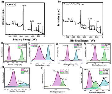 |
| | Fig. 5 (a) XPS spectra of Cs2NaInCl6, (b) Cs2Na0.6Ag0.4In0.9Bi0.1Cl6:0.15Mn2+, (c) Cs 3d, (d) Na 1s, (e) In 3d, (f) Ag 3d, (g) Bi 4f , (h) Cl 2p and (i) Mn 2p. | |
 |
| | Fig. 6 Thermo-gravimetric analysis of Cs2Na0.6Ag0.4In0.9Bi0.1Cl6:0.15Mn2+ sample. | |
3.3. Thermogravimetric analysis
Fig. 6 depicts the thermogravimetric analysis of the as-prepared optimised sample of Cs2Na0.6Ag0.4In0.9Bi0.1Cl6:0.15Mn2+. TGA analysis is performed from room temperature to 800 °C with a N2 atmosphere to analyse the thermal stability of the prepared sample. The decomposition of the sample occurs in two steps/stages. Minor loss of weight (∼15%) is observed beyond 548 °C. A major weight loss of 35% occurs from 450 °C to 600 °C, beyond which an abrupt weight loss of ∼50% occurs beyond 600 °C to 800 °C. Thus, the sample exhibits good thermal stability of up to 500 °C compared to the halide-based perovskites.47,48
3.4. Optical properties
3.4.1. UV-vis diffusion reflectance spectroscopy. The synthesised pristine Cs2NaInCl6 and optimised sample of Cs2Na0.6Ag0.4In0.9Bi0.1Cl6:0.15Mn2+ samples were subjected to UV-visible diffuse reflectance spectroscopy. The absorption intensity of the intrinsic and optimised samples was observed in the range of 200–350 nm, as shown in Fig. 7(a). The optical bandgap of the DPs is obtained using the Kubelka–Munk method and the Tauc plot relation. The optical band gap of Cs2NaInCl6 and Cs2Na0.6Ag0.4In0.9Bi0.1Cl6:0.15Mn2+ structure is calculated, as shown in Fig. 7(b) and (c). The band gap of the material can also be calculated using the following formula:
where α denotes the absorption coefficient, h denotes Planck's constant, C denotes the proportionality constant, v denotes the frequency of light, Eg denotes the band gap and 1/n refers to 1/2 or 2, which denotes that the material possesses either a direct or an indirect band gap, respectively.34 The pristine Cs2NaInCl6 and Cs2Na0.6Ag0.4In0.9Bi0.1Cl6:0.15Mn2+ samples possess an indirect band gap with wide optical band gaps Eg = 5.1 eV and Eg = 3.01 eV, respectively, which is very similar to the literature survey.49 As silver (Ag+) and bismuth (Bi3+) are incorporated into the lattice, there is a huge reduction in the bandgap. As the silver content in the DPs increases, there is a high possibility for an increase in the interaction between Ag 4d and the valence band of the DP lattice, which leads to a reduction in the band gap by ∼1.4 eV, as shown in Fig. S5(a).†12,50 Further, the incorporation of Bi causes a reduction in the band gap from 3.7 eV to 3.01 eV, as shown in Fig. S5(b),† which explains the redshift in the emission wavelength.34,51 After the incorporation of Mn into the optimised lattice, no change in the band gap is observed.
 |
| | Fig. 7 (a) Diffusion reflectance UV-vis spectra and (b) Tauc plot of Cs2NaInCl6 and (c) Cs2Na0.6Ag0.4In0.9Bi0.1Cl6:0.15Mn2+. | |
3.4.2. Photoluminescence spectroscopy. The Cs2NaInCl6 host lattice was found to exhibit a very weak blue emission with a λmax of 450 nm under excitation of 350 nm owing to its parity-forbidden transitions, as shown in Fig. 8(a) represented as a black curve. Alloying Ag+ at the Na+ site causes an increase in the emission intensity with λmax at 587 nm, and progressive broadening in the emission peak is observed. A series of samples of Cs2Na1−xAgxInCl6 (x varies from 0 to 1) is shown in Fig. 8(a). At a concentration of 0.4 mmol of Ag, a broad and highly intense peak was observed with emission maxima at 587 nm. Further, as Ag+ concentration increased, a gradual reduction in the emission intensity was observed. The incorporation of 0.4 mmol of Ag+ into the intrinsic sample increases the photoluminescence quantum yield (PLQY) of the lattice by ∼12%. Thus, a 0.4 mmol concentration of Ag+ was found to be optimum. Owing to the similar even parity of the valence band maxima and the conduction band minima at the Γ point, the dipole transition in the band edge states of Cs2NaInCl6 is parity forbidden, which leads to low band-edge emission with a very low PLQY that is <3%.52–54 Because Ag+ is alloyed at the Na+ site, this leads to a significant enhancement in the PLQY of the DPs, which indicates that the parity-forbidden transition is broken successfully.
 |
| | Fig. 8 PL emission spectra of (a) Cs2Na(1−x)AgxInCl6 and (b) Cs2Na0.6Ag0.4In(1−y)BiyCl6. (c) and (d) PLE and PL of Cs2Na0.6Ag0.4In0.9Bi0.1Cl6:0.15Mn2+. | |
Keeping the concentration of Ag constant (0.4 mmol), a series of samples with variations in Bismuth were prepared, and their PL was recorded, as shown in Fig. 8(b). The optimum concentration of Bi was found to be 0.1 mmol. The addition of Bismuth causes a considerable red shift in the emission spectra from 587 to 614 nm, with the full width at half maxima (FWHM) of 204 nm.55 The incorporation of Bi3+ into the lattice helps enhance the broadband emission from 400 to 750 nm. Bi3+ ions form passivating defects inside the crystal and help to increase the PLQY of Cs2Na0.6Ag0.4In0.7Bi0.1Cl6. Table S1† shows the PLQY of all the optimised samples. Bi3+ introduction also leads to the redshift in the luminescent peak position34,50 and helps extend the excitation till ∼360 nm,55 and PLQY was found to be ∼29.4%. To further enhance the red emission, Mn2+ ion is used as a dopant in the optimised Cs2Na0.6Ag0.4In0.9Bi0.1Cl6. We prepared a series of samples with Mn concentrations ranging from 0.07 to 0.21 mmol. Beyond 0.15 mmol, the photoluminescence intensity was found to reduce, and a slight blue shift in the emission spectra was also observed, as shown in Fig. S5 in the ESI file.† After the incorporation of the optimised amount of Mn2+ (0.15 mmol) into Cs2Na0.6Ag0.4In0.9Bi0.1Cl6, a shift is observed in the emission peak at 665 nm, as shown in Fig. 8(d) and (c), which represent the PLE spectra of Cs2Na0.6Ag0.4In0.9Bi0.1Cl6:0.15Mn2+. In this lattice, Mn2+ ions primarily serve as luminescent centers, enabling strong orange-red photoluminescence and further shifting in the emission peak position of Cs2Na0.6Ag0.4In0.9Bi0.1Cl6 sample by 51 nm. The Mn2+ ions, when incorporated into the lattice, typically occupy octahedral sites and exhibit a characteristic 4T1 → 6A1 transition attributed to the spin-forbidden transition of Mn2+.24,56 After the incorporation of Mn2+ in the optimised lattice, the PLQY reached 44.9%. The broad emission peak of the prepared DPs is observed due to the Self Trapped Exciton (STE)-based emission, which can be explained using Scheme 2. Cs2NaInCl6 exhibits weak blue emission at a wavelength of 450 nm with a low PL intensity that results in optically forbidden transition, which is accompanied by dark STEs of halide double perovskites.57 The broad emission in Cs2Na0.6Ag0.4In0.9Bi0.1Cl6 is due to the inherent property of STE-based emission, which is possessed by the host lattice (transition 3). When Mn2+ is introduced into the lattice, an energy shift occurs from the STEs to 4T1 to 6A1 (transition 4). This leads to the red shift in the emission peak position, and a very distinctive peak position at 665 nm is obtained (transition 5) in Scheme 2.1
 |
| | Scheme 2 Schematic of the self-trapped exciton emission mechanism in perovskites. | |
3.4.3. Time-resolved photoluminescence spectroscopy. To understand the excited state dynamics of the intrinsic (Cs2NaInCl6) and optimised sample (Cs2Na0.6Ag0.4In0.9Bi0.1Cl6:0.15Mn2+), time-resolved photoluminescence spectra were studied, as shown in Fig. 9(a) and (b). Cs2NaInCl6 exhibits an instantaneous rise in the PL signal, followed by a quick decay. However, Cs2Na0.6Ag0.4In0.9Bi0.1Cl6:0.15Mn2+ shows a gradual decay. The samples exhibit a double exponential fitting, as described by the following expression:58,59
where I and I0 denote the intensities of the photoluminescence emissions at time t and at t = 0. Moreover, τ1 and τ2 are the decay constants, indicating the fast and slow lifetimes for the exponential components, respectively. A1 and A2 are known as the fitting constants or weighting constant parameters. The decay constant of the prepared DPs can be fitted using a bi-exponential equation. The average value of lifetime can be calculated by applying the Inokuti–Hirayama model using the following equation:52
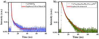 |
| | Fig. 9 (a) TRPL of Cs2NaInCl6 and (b) Cs2Na0.6Ag0.4In0.9Bi0.1Cl6:0.15Mn2+. | |
The calculated average lifetime of the prepared DPs (Cs2Na0.6Ag0.4In0.9Bi0.1Cl6:0.15Mn2+) was found to be 2 μs. Decay parameters are listed in Table 2.
Table 2 Fitting parameters of TRPL decay curves used for calculating average lifetime
| Sample |
τ1 |
τ2 |
A1 |
A2 |
Avg. lifetime |
| Cs2NaInCl6 |
316.68 |
4187.522 |
1.49 |
0.03 |
1 ns |
| Cs2Na0.6Ag0.4In0.9Bi0.1Cl6:0.15Mn2+ |
2261.15 |
10![[thin space (1/6-em)]](https://www.rsc.org/images/entities/char_2009.gif) 643.82 643.82 |
15.36 |
0.10 |
2 ns |
3.4.4. Temperature-dependent PL spectra. The prepared DPs (Cs2Na0.6Ag0.4In0.9Bi0.1Cl6:0.15Mn2+) are subjected to temperature-dependent photoluminescence spectroscopy (TDPL) to understand the thermal property and the electron-phonon coupling mechanism. Fig. 10(a) shows the TDPL of the as-prepared optimised sample at different temperatures starting from room temperature to 150 °C. Emission intensity was found to decrease as temperature increased owing to the non-radiative radiations of electrons from the excited state to the ground state.40,60,61 At a high temperature of 150 °C, the emission intensity of the perovskite was found to reduce by 76% of its initial value. No shift in the emission spectra was observed as the temperature increased. The Arrhenius plot shown in Fig. 10(b) is plotted against the inverse of the absolute temperature. The Arrhenius equation is given by58,62
where Io is the emission intensity that is observed at room temperature, IT is the emission intensity of temperature t, C is the arbitrary constant and KB is the Boltzmann constant value of 8.617 × 10⁻⁵ eV K−1. The activation energy of the synthesised material determined by calculating the slope of the plot between ln(I0/IT) − 1 and 1/KBT is 0.465 eV.
 |
| | Fig. 10 (a) Temperature-dependent PL spectra and (b) Arrhenius plot of Cs2Na0.6Ag0.4In0.9Bi0.1Cl6:0.15Mn2+. | |
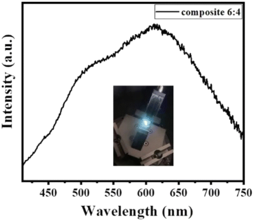
3.4.5. Spectral parameters of composite of DP with BAM:Eu2+. To obtain complete spectral coverage in the visible region, a composite of DP with BAM:Eu2+ was prepared as explained in the Subsection 2.3. To obtain the optimised ratio, DP with BAM:Eu2+ was blended in various ratios of 2:8, 3:7, 4:6, 5:5, 6:4 7:3 and 8:2 by weight%. The room temperature PL emission of all the composite samples was recorded, as shown in Fig. S6.† Various spectral parameters, such as CIE coordinates, CRI values, and CCT, were calculated, as shown in Table 3. A high CRI of ∼87 was obtained for the DP:BAM composite of 6:4 by weight, as shown in Fig. 11. CIE color coordinates were calculated using the wavelength equidistant method. The as-prepared composite was found to have CIE coordinates of (0.37, 0.39), which is quite close to that of ideal white light (0.33, 0.33). The CIE plots of all the composites are shown in Fig. S7.† The color-correlated temperature was found to be 4453.5 K, which falls under the natural white light category. The CCT of the composite can be tuned from warm (2935 K) to cool white (6789 K).
Table 3 CCT, CIE and CRI of various composites
| WLEDs |
Mass ratio of BAM:perovskites |
CCT/K |
CIE (x,y) coordinates |
CRI |
| 1 |
0:10 |
2935.45 |
(0.44, 0.40) |
68.9 |
| 2 |
2:8 |
3086.65 |
(0.42, 0.43) |
78.2 |
| 3 |
3:7 |
3198.13 |
(0.41, 0.42) |
82.7 |
| 4 |
4:6 |
3319.18 |
(0.40, 0.42) |
80.1 |
| 5 |
5:5 |
3599.35 |
(0.38, 0.41) |
82.1 |
| 6 |
6:4 |
4453.52 |
(0.37, 0.39) |
87.4 |
| 7 |
7:3 |
3758.60 |
(0.34, 0.39) |
81 |
| 8 |
8:2 |
6789.64 |
(0.27, 0.34) |
78.1 |
 |
| | Fig. 11 Room temperature PL emission spectra of the optimised BAM: DP sample with 6:4 composition by weight (inset: image of BAM: DP under 365nm). | |
4. Conclusion
In this study, we successfully synthesised pristine Cs2NaInCl6 by applying a facile co-precipitation method. To enhance the photoluminescence properties, Ag and Bi alloying was performed at the Na and In sites to obtain optimised sample.
Cs2Na0.6Ag0.4In0.9Bi0.1Cl6. It was observed that the incorporation of a 0.4 mmol concentration of Ag alloying enhanced the emission signal 10 times, with peak maxima at 587 nm. Further, Bi ions cause a red shift in the emission spectra from 587 to 614 nm and increase the FWHM by 204 nm. By incorporating Bi and Ag, PLQY was found to increase by 29.4%. Broad emission owing to the 4T1 → 6A1 transition of Mn2+ ions was observed at 665 nm. The sample also exhibits good thermal stability with a high activation energy of 0.5 eV, and 43% of the initial PL emission intensity stays intact even at a high temperature of 100 °C. Detailed structural, optical, morphological and compositional analyses were conducted for the pristine and optimised samples. PLQY was found to increase from 1.8% to 44.9% upon alloying and doping the pristine sample. Spectral parameters (CIE coordinates of (0.37, 0.39), CCT of 4453.52 K, and CRI of 87.4) were calculated. Thus, combined with blue-emitting phosphors, Cs2Na0.6Ag0.4In0.9Bi0.1Cl6:Mn2+ is a potential material for enhancing the CRI of WLEDs owing to its broad red emission extending in the blue region at 475 nm. The scope of future work involves developing double perovskite materials to obtain complete coverage in the visible spectra.
Data availability
The data supporting the findings of this study are available within the article and its ESI.†
Author contributions
D. B.: conception, experimentation, analysis, writing manuscript; G. S.: review and final editing.
Conflicts of interest
Authors declare no conflicts of interest.
Acknowledgements
The authors would like to acknowledge Centre for Nanotechnology Research, VIT Vellore, for their research facilities and School of Advanced Sciences (SAS), VIT Vellore, for the financial support.
References
- M. Hu, S. Li, J. Liu and J. Li, Broadband emission of double perovskite, Opt. Lett., 2019, 44, 4757–4760, DOI:10.1364/OL.44.004757.
- C. Jiawei, et al., Perovskite White Light Emitting Diodes: Progress, Challenges, and Opportunities, ACS Nano, 2021, 15(11), 17150–17174 CrossRef PubMed.
- B. Zhang, et al., Colloidal Bi-Doped Cs2Ag1-xNaxInCl6Nanocrystals: Undercoordinated Surface Cl Ions Limit their Light Emission Efficiency, ACS Mater. Lett., 2020, 2, 1442–1449 CrossRef PubMed.
- P. Han, et al., Lead-Free Sodium–Indium Double Perovskite Nanocrystals through Doping Silver Cations for Bright Yellow Emission, Angew. Chem., 2019, 131, 17391–17395 CrossRef.
- Y. Wu, X. Li and H. Zeng, Lead-Free Halide Double Perovskites: Structure, Luminescence, and Applications, Small Struct., 2021, 2(3), 2000071 CrossRef.
- J. Yao, L. Xu, S. Wang and J. Song, Metal halide perovskites-based white light-emitting diodes, JPhys Photonics, 2022, 4, 042001 CrossRef.
- S. Wang, et al., Novel SrMg2La2W2O12:Mn4+ far-red phosphors with high quantum efficiency and thermal stability towards applications in indoor plant cultivation LEDs, RSC Adv., 2018, 30191–30200, 10.1039/c8ra06134c.
- M. Liu, B. Shen, K. Wang and J. Zhong, RSC Adv., 2019, 20742–20748, 10.1039/c9ra03410b.
- X. Wu, et al., Photoluminescence, energy transfer, color tunable properties of Sr3La(BO3)3:Ce, Tb phosphors, J. Alloys Compd., 2018, 730, 521–527 CrossRef CAS.
- W. Geng, X. Zhou, J. Ding and Y. Wang, NaBaY(BO3)2:Ce3+,Tb3+: A novel sharp green-emitting phosphor used for WLED and FEDs, J. Am. Ceram. Soc., 2018, 101, 4560–4571 CrossRef CAS.
- D. Haranath, et al., Rare-earth free yellow-green emitting NaZnPO4:Mn phosphor for lighting applications, Appl. Phys. Lett., 2012, 101, 221905 CrossRef.
- S. Dan, Origin of bandgap bowing in Cs2Na1− x Ag x BiCl6 double perovskite solid-state alloys: a paradigm through scanning tunneling spectroscopy, J. Phys.: Condens. Matter, 2021, 33(48), 485701 CrossRef CAS.
- Y. Zhou, Impact of Eu3+ dopants on optical spectroscopy of Ce3+: Y3Al5O12-embedded transparent glass-ceramics, J. Am. Ceram. Soc., 2015, 98(8), 2445–2450 CrossRef CAS.
- X. B. Li, W. B. Dai, K. Nie, S. P. Li and M. Xu, Investigation on optical properties of borate Sr3Y2B4O12: Ce/Tb/Sm and its application in wLEDs, J. Lumin., 2023, 263, 120038 CrossRef CAS.
- F. Wang, H. Pan, W. Mao and D. Wang, Heliyon Optimizations of luminescent materials for white light emitting diodes toward healthy lighting, Heliyon, 2024, 10, e34795 CrossRef CAS PubMed.
- W. Chen, et al., Carbon dots embedded in lead-free luminescent metal halide crystals toward single-component white emitters, Sci. China Mater., 2022, 65, 2802–2808 CrossRef CAS.
- S. Thapa, G. C. Adhikari, H. Zhu, A. Grigoriev and P. Zhu, Zn-Alloyed All-Inorganic Halide Perovskite-Based White Light-Emitting Diodes with Superior Color Quality, Sci. Rep., 2019, 9, 18636 CrossRef CAS PubMed.
- S. B. Kundu, P. Pallavi and A. Patra, Chem.–Eur. J., 2020, 26(25), 5557–5582 CrossRef PubMed.
- S. Mukherjee and P. Thilagar, Organic White-Light Emitting Materials, Dyes Pigm., 2014, 110, 2–27 CrossRef.
- P. Cai, X. Wang, H. J. Seo and X. Yan, Bluish-white-light-emitting diodes based on two-dimensional lead halide perovskite (C6H5C2H4NH3)2PbCl2Br2, Appl. Phys. Lett., 2018, 112, 153901 CrossRef.
- Y. H. Song, et al., Design of long-term stable red-emitting CsPb(Br0.4, I0.6)3 perovskite quantum dot film for generation of warm white light, Chem. Eng. J., 2017, 313, 461–465 CrossRef.
- F. Igbari, Z.-K. Wang and L.-S. Liao, Progress of Lead-Free Halide Double Perovskites, Adv. Energy Mater., 2019, 9, 1803150 CrossRef.
- R. L. Z. Hoye, J. Hidalgo, R. A. Jagt, T. Fix and J. L. Macmanus-driscoll, The Role of Dimensionality on the Optoelectronic Properties of Oxide and Halide Perovskites, and their Halide Derivatives, Adv. Energy Mater., 2021, 2100499 Search PubMed.
- L. Zhang, et al., Investigation on lead-free Mn-doped Cs 2 NaInCl 6 double perovskite phosphors and their optical properties, Opt. Mater., 2021, 122, 111802 CrossRef.
- H. Tang, et al., Lead-Free Halide Double Perovskite Nanocrystals for Light-Emitting Applications: Strategies for Boosting Efficiency and Stability, Adv. Sci., 2021, 3, 1–23 Search PubMed.
- M. Tabassum, Q. Zia, Y. Zhou, M. J. Reece and L. Su, A review on advances in doping with alkali metals in halide perovskite materials, SN Appl. Sci., 2021, 3, 1–15 Search PubMed.
- J. Chen, et al., Perovskite White Light Emitting Diodes: Progress, Challenges, and Opportunities, ACS Nano, 2021, 15, 17150–17174 CrossRef PubMed.
- Y. Wang, et al., High color rendering index trichromatic white and red LEDs prepared from silane-functionalized carbon dots, J. Mater. Chem. C, 2017, 5, 9629–9637 RSC.
- P. Bodrogi, S. Brückner, N. Krause and T. Q. Khanh, Semantic interpretation of color differences and color-rendering indices, Color Res. Appl., 2014, 39, 252–262 CrossRef.
- A. K. Vishwakarma, et al., Emerging cool white light emission from Dy3+ doped single phase alkaline earth niobate phosphors for indoor lighting applications, Dalton Trans., 2015, 44, 17166–17174 RSC.
- N. Ohta, and A. Robertson, Colorimetry: fundamentals and applications, John Wiley & Sons, 2006 Search PubMed.
- S. Westland,The CIE System, in Handbook of Visual Display Technology, ed. J. Chen, W. Cranton, M. Fihn, Springer, Cham, 2016, DOI:10.1007/978-3-319-14346-0_11.
- H. A. Badran, et al., Study of Colorimetric properties of Ethidium bromide dye-doped PVP/DNA film, J. Phys.: Conf. Ser., 2021, 1963(1), 012102 CrossRef CAS.
- K. Peng, et al., The synthesis of lead-free double perovskite Cs2Ag0.4Na0.6InCl6 phosphor with improved optical properties via ion doping, J. Alloys Compd., 2022, 891, 161978 CrossRef CAS.
- B. Ke, et al., Homo- and Heterovalent Doping-Mediated Self-Trapped Exciton Emission and Energy Transfer in Mn-Doped Cs2Na1–xAgxBiCl6 Double Perovskites, J. Phys. Chem. Lett., 2020, 11, 340–348, DOI:10.1021/acs.jpclett.9b03387.
- M. Jeevaraj, S. Sudhahar, N. Nallamuthu, P. Devendran and S. Saravanakumar, Physica B : Condensed Matter Solution processed Mn 2 + doped Cs 2 AgInCl 6 lead free double perovskite as a potential light emitting material, Phys. B, 2023, 653, 414679 CrossRef CAS.
- G. Wang, et al., Observation of Extraordinary Vibration Scatterings Induced by Strong Anharmonicity in Lead-Free Halide Double Perovskites, Adv. Sci., 2025, 12, 2408149 CrossRef CAS.
- Q. Chen, et al., single-composition white-light emitting phosphors and multimodal optical, J. Lumin., 2023, 258, 119783 CrossRef CAS.
- P. Han, et al., Lead-Free Sodium – Indium Double Perovskite Nanocrystals through Doping Silver Cations for Bright Yellow Emission, Angew. Chem. Int. Ed., 2019, 1–6, DOI:10.1002/anie.201909525.
- X. Li, et al., Facile Melting-Crystallization Synthesis of Cs2NaxAg1–xInCl6: Bi Double Perovskites for White Light-Emitting Diodes, Inorg. Chem., 2022, 61, 5040–5047, DOI:10.1021/acs.inorgchem.1c03996.
- B. Zhou, et al., Efficient White Photoluminescence from Self- Trapped Excitons in Sb 3+/Bi 3+ -Codoped Cs 2 NaInCl 6 Double Perovskites with Tunable Dual-Emission, ACS Energy Lett., 2021, 6(9), 3343–3351 CrossRef CAS.
- M. Jeevaraj, P. Devendran, N. Nallamuthu, S. Sudhahar and M. K. Kumar, Influence of Mn2+ doping on the optical properties of Cs2AgBiCl6 double perovskite luminescent phosphors, J. Mater. Sci.:Mater. Electron., 2023, 34, 65 CrossRef CAS.
- K. Kumar, Extrinsic electronic states to tune the luminescence and bonding nature of Cs 2 NaInCl 6 double perovskite, Mater. Chem. Phys., 2024, 311, 128569 CrossRef.
- M. Kalapsazova, R. Stoyanova, E. Zhecheva, G. Tyuliev and D. Nihtianova, Sodium deficient nickel–manganese oxides as intercalation electrodes in lithium ion batteries, J. Mater. Chem. A, 2014, 2, 19383–19395 RSC.
- W. Jiang, et al., Improved optical properties of lead-free double perovskite Cs2NaBiCl6 nanocrystal via K ions doping, J. Alloys Compd., 2023, 960, 170871 CrossRef CAS.
- H. Wang, et al., Lead – free – perovskite films with broad warm - yellow emission for lighting applications, Sci. Rep., 2024, 1–14, DOI:10.1038/s41598-024-65492-5.
- L. Zhang, et al., Investigation on lead-free Mn-doped Cs2NaInCl6 double perovskite phosphors and their optical properties, Opt. Mater., 2021, 122, 111802 CrossRef CAS.
- R. Zeng, et al., Highly Efficient Blue Emission from Self-Trapped Excitons in Stable Sb 3+ -Doped Cs 2 NaInCl 6 Double Perovskites, J. Phys. Chem. Lett., 2020, 11(6), 2053–2061 CrossRef CAS PubMed.
- H. You, et al., Tunable-Color UV-Excitation Sb3+/(Bi3+, Ag+)-Doped Cs2NaInCl6 Perovskite for High-Color-Rendering Full-Spectrum w-LEDs, ACS Appl. Opt. Mater., 2023, 1, 788–794 CrossRef CAS.
- F. Liu, et al., White light emission with unity efficiency from Cs2Na1−xAgxIn1−yBiyCl6 double perovskites: the role of bismuth and silver, J. Mater. Chem. C, 2022, 14232–14241, 10.1039/d2tc02919g.
- H. You, et al., Perovskite for High-Color-Rendering Full-Spectrum w - LEDs, ACS Appl. Opt. Mater., 2023, 1(3), 788–794 CrossRef.
- J. Zhou, et al., Manipulation of Bi 3 +/In 3 + Transmutation and Mn 2 + -Doping Effect on the Structure and Optical Properties of Double Perovskite Cs 2 NaBi 1- x In x Cl 6, Adv. Opt. Mater., 2019, 1801435 CrossRef.
- H. Li, et al., Double perovskite Cs2NaInCl6 nanocrystals with intense dual-emission via self-trapped exciton-to-Tb3+ dopant energy transfer, J. Mater. Chem. C, 2022, 10, 10609–10615 RSC.
- R. Ahmad, et al., Uncovering the Role of Trioctylphosphine on Colloidal and Emission Stability of Sb-Alloyed Cs2NaInCl6 Double Perovskite Nanocrystals, ACS Appl. Mater. Interfaces, 2021, 13, 47845–47859 CrossRef.
- M. B. Gray, J. D. Majher, T. A. Strom and P. M. Woodward, Broadband White Emission in Cs2AgIn1–xBixCl6 Phosphors, Inorg. Chem., 2019, 58, 13403–13410, DOI:10.1021/acs.inorgchem.9b02299.
- L. Chen, et al., materials Mn 2 + -doped Cs 2 NaInCl 6 double perovskites and their photoluminescence properties, J. Mater. Sci., 2021, 56, 8048–8059 CrossRef.
- Y. Gao, S. Xu and B. Chen, Lead-free double perovskite Cs2NaInCl6 nanocrystals doped with Sb3+ and Tb3+ for copper ions detection in lubricating oil, Spectrochim. Acta, Part A, 2024, 308, 123683 CrossRef.
- A. M. Achari, V. Perumalsamy, G. Swati and A. Khare, SrAl2O4:Eu2+,Dy3+ Long Afterglow Phosphor and Its Flexible Film for Optomechanical Sensing Application, ACS Omega, 2023, 8, 45483–45494 CrossRef PubMed.
- P. Vanishree and G. Swati, Enhanced photoluminescence in (Ca, Zn)TiO3: Pr3+ afterglow phosphor for anti-counterfeiting application, J. Mater. Sci.:Mater. Electron., 2024, 35, 597 CrossRef.
- X. Huang, Y. Matsushita, H. Sun and N. Shirahata, Nanoscale Adv., 2022, 3091–3100, 10.1039/d2na00238h.
- P. Kanapathi, N. Ravi and T. Appadurai, Investigation on Structurally Engineered Cs2AgInCl6 via Alloying (Na+)/Doping (Cr3+, Mn2+) for Flexible Phosphor-Based White Light Devices and Latent Fingerprint Detection Application, ACS Appl. Energy Mater., 2024, 7, 10026–10036 CrossRef.
- P. Li, et al., Temperature dependent red luminescence from a distorted Mn4+ site in CaAl4O7:Mn4+, Opt. Express, 2013, 21, 18943–18948 CrossRef PubMed.
|
| This journal is © The Royal Society of Chemistry 2025 |
Click here to see how this site uses Cookies. View our privacy policy here. 
 Open Access Article
 This Open Access Article is licensed under a Creative Commons Attribution-Non Commercial 3.0 Unported Licence
 *
*