
 Open Access Article
 This Open Access Article is licensed under a
 Creative Commons Attribution 3.0 Unported Licence
Optimized nanostructured In2O3 gas sensors: harnessing annealing-induced defects and oxygen vacancies for ultra-sensitive and selective H2S detection at trace levels†
Tanya Sood a,
Ramseena Thundiyila,
Anushaa,
Saikat Chattopadhyayb and
P. Poornesh*a
a,
Ramseena Thundiyila,
Anushaa,
Saikat Chattopadhyayb and
P. Poornesh*a
aDepartment of Physics, Manipal Institute of Technology, Manipal Academy of Higher Education, Manipal 576104, India. E-mail: poornesh.p@manipal.edu; poorneshp@gmail.com
bDepartment of Physics, School of Basic Sciences, Manipal University Jaipur, Jaipur 303007, India
First published on 19th May 2025
Abstract
Achieving selectivity and high sensitivity for specific analytes at trace levels remains a significant challenge for chemiresistive gas sensors. In this study, nanostructured indium oxide (In2O3) gas sensors were synthesized via spin coating for detection of hydrogen sulphide (H2S) gas at trace levels. The influence of annealing temperature on the gas sensing performance for the deposited nanostructured gas sensors was systematically investigated. The sensor annealed at 350 °C exhibited outstanding performance, with rapid response time of (17 ± 1) seconds for H2S gas concentrations of 4 ppm, at an optimal operating temperature of 250 °C. Additionally, it achieved an exceptional sensing response of (36.52 ± 2.02)% and (97.89 ± 0.08)% for 0.5 ppm and 4 ppm H2S gas respectively. The remarkable sensing performance is attributed to the presence of structural defects, voids and oxygen vacancies, which enhance gas adsorption and reactivity. These findings demonstrate that In2O3 nanostructured gas sensors are highly effective for the reliable detection and monitoring of H2S gas in practical applications.
1. Introduction
The rapid expansion of industry, coupled with a growing global population, has led to a significant decline in air quality due to the increasing release of harmful pollutants. Among these pollutants, particulate matter (PM2.5 and PM10), nitrogen dioxide (NO2), carbon monoxide (CO), ammonia (NH3), sulfur dioxide (SO2), and hydrogen sulfide (H2S) pose serious threats to both human health and the environment.1 H2S is highly toxic even at low concentrations, making it a critical target for air quality monitoring systems. It is emitted from both natural and anthropogenic sources, including sewage treatment plants, volcanic activity, oil refining, and natural gas processing.2 Due to its extreme toxicity, both acute and chronic exposure can lead to severe respiratory distress, neurological impairment, and, in high concentrations, fatalities. Recognizing these dangers, regulatory agencies such as the Occupational Safety and Health Administration (OSHA) in the United States have set strict exposure limits. OSHA enforces a short-term exposure limit (STEL) of 15 ppm for a 10 minutes period, while the American Conference of Governmental Industrial Hygienists (ACGIH) has established a threshold limit value (TLV-TWA) of 1 ppm for an 8 hours workday. These regulations underscore the urgent need for reliable H2S detection systems.3,4To mitigate the risks associated with H2S exposure, accurate and continuous monitoring is essential. Conventional gas detection systems, such as electrochemical and optical sensors, have been widely used but suffer from limited lifespan, high power consumption, and susceptibility to environmental interference.5 Therefore, there is an increasing demand for lightweight, compact, energy-efficient, and highly selective gas sensors that can operate reliably in various environments, including industrial facilities, confined spaces, and urban settings.6 Sensors must also exhibit high sensitivity for low-concentration detection, long-term stability, and cost-effectiveness to ensure widespread deployment. Developing such advanced sensors is crucial for the early detection of H2S, allowing preventive actions before it reaches hazardous levels.7
Among various gas sensing materials, metal oxide semiconductors (MOS) have emerged as promising candidates due to their low-cost fabrication, high sensitivity, and fast response times. MOS materials such as WO3,8 SnO2,9 In2O3,10 Fe2O3,11 CuO,12 ZnO,13 and NiO14 are widely used for gas sensing applications, benefiting from their excellent thermal stability and well-understood sensing mechanisms. Among these metal oxides, In2O3 stands out as a highly promising gas sensing material due to its exceptional electrical conductivity, chemical stability, tuneable surface properties, and ability to detect a wide range of toxic gases, including NH3,15 CO,16 H2S,17,18 and NO2.19 Its n-type semiconducting behaviour, with a direct band gap of 3.6 eV and an indirect band gap of 2.6 eV, enables efficient charge carrier transport, making it suitable for gas sensing applications as well as its use in transparent conducting oxides (TCOs),20 optoelectronics, light-emitting diodes (LEDs), and electrochromic devices.21 Additionally, its ability to absorb and transmit visible light contributes to its applicability in electrical switching and other advanced electronic applications.22 The presence of oxygen vacancies enhances its sensing performance, improving response time and sensitivity.23 Despite these advantages, challenges remain in optimizing sensor selectivity, response stability, and large-area fabrication, necessitating further investigation into novel deposition techniques and material modifications. Extensive research has been conducted to develop In2O3 based gas sensors, with a focus on improving their sensitivity, selectivity, and stability.24 Various deposition techniques are employed to fabricate In2O3 thin films, each offering unique advantages in terms of film quality, scalability, and cost-effectiveness. These include physical methods such as thermal evaporation, e-beam evaporation, sputtering, pulsed laser deposition (PLD)25 and chemical techniques such as spray pyrolysis,26 thermal hydrolysis,27 dip coating, electrospinning, sol–gel,28 spin coating,29 solvothermal synthesis, and hydrothermal processing.30 Among these, spin coating is widely recognized as an efficient technique for depositing uniform thin films over large areas due to its precise control over chemical composition, high purity, reproducibility, and cost efficiency.29
The gas sensing properties of In2O3 thin films are heavily influenced by film morphology (nanorods, nanosheets, nanoflowers) and microstructure, both of which are determined by the choice of deposition method, processing conditions, and subsequent annealing treatments. Annealing is a crucial post-deposition step that enhances crystallinity, eliminates structural defects, improves film uniformity, and increases grain size, thereby significantly impacting gas adsorption and desorption kinetics.31 Moreover, annealing leads to an increase in oxygen vacancies, which act as electron donors, improving charge transport and overall sensor performance. These modifications collectively contribute to higher sensitivity, faster response and recovery times, and improved long-term stability, making annealed In2O3 an excellent candidate for gas detection applications. Several studies have demonstrated the significant influence of annealing temperature on gas sensing performance. Ravikumar T. et al. investigated ZnFe3O4 films deposited via spray pyrolysis, showing a fivefold increase in NH3 sensing response upon annealing at 400 °C, compared to the as-deposited film.32 Similarly, Sarf F. et al. synthesized α-Fe2O3 thin films via spin coating and observed that annealing at 600 °C yielded a 10% enhancement in CO sensing response at ambient temperature, attributing the improvement to better crystallization and increased porosity.33 Additionally, Gupta et al. employed the sol–gel method to synthesize NiO powders and reported a 244.4% increase in LPG gas sensing response after annealing at 500 °C, demonstrating that optimized annealing conditions significantly enhance sensitivity and selectivity in metal oxide gas sensors.34
Building upon these findings, this study systematically investigates the effect of annealing temperature on the structural, morphological, optical, and H2S gas sensing characteristics of spin-coated In2O3 thin films. The annealing process plays a pivotal role in modulating the crystallinity, surface roughness, and oxygen vacancy concentration, which directly affect the sensor's performance. By varying the annealing temperature, its impact on film composition, charge carrier dynamics, and gas adsorption sites can be systematically evaluated. This study presents an optimized In2O3-based chemiresistive gas sensor for highly selective and sensitive H2S detection by systematically tuning the annealing temperature (250–400 °C). The results demonstrate that the annealing at 350 °C significantly enhances the sensor response (97.89 ± 0.08%) due to improved crystallinity, surface interactions and oxygen vacancy modulation. The sensor exhibits a low detection limit of 0.5 ppm, rapid response (17 ± 1 s at 4 ppm H2S), and excellent repeatability over multiple cycles, ensuring reliability. Additionally, the study evaluates the effect of temperature on sensor performance, revealing that 250 °C is the optimal operating temperature, balancing adsorption and desorption kinetics. These findings reinforce the critical role of annealing in optimizing In2O3 based gas sensors and underscore the potential of spin-coated In2O3 thin films as highly effective, selective, and stable H2S detectors for real-world applications in environmental monitoring and industrial safety.
2. Experimental details
2.1. Preparation of In2O3 nanostructured thin films
Acetone (CH3COCH3), isopropanol (C3H8O), 2-methoxyethanol (C3H8O2), and indium(III) nitrate hydrate [In(NO3)3·xH2O] (99.99% pure), were procured from MERCK. Deionized water (DI) with a resistivity of 18.3 MΩ was used exclusively throughout the process. Microscopic glass slides were obtained from Labtech. These chemicals and materials were employed in the preparation of the precursor solution for the spin coating method.The cleaning process involved sequentially treating the substrates with soap solution, DI water, isopropanol (IPA), and acetone, individually for 10 minutes in an ultrasonic bath. Following the cleaning steps, the substrates underwent air drying with a flow of nitrogen. To further remove organic impurities and minimize surface roughness, ozone treatment was applied for 15 minutes, leading to a more uniform and cleaner surface. 0.2 M of the aqueous precursor solution was then prepared utilizing indium nitrate hydrate, and 2-methoxyethanol. The solution was continuously stirred at 60 °C for 24 hours to achieve a transparent, and homogeneous mixture, followed by aging at room temperature for another 24 hours. The aged precursor solution was coated onto the glass substrate utilizing the spin coating method at a precise speed of 2000 rpm for 30 seconds. The films were subsequently heated at 250 °C for 5 minutes to remove the solvent. This process was performed for 15 times to achieve the desired thickness of 250–300 nm. Subsequently, the films were annealed at temperatures: 250 °C, 300 °C, 350 °C, and 400 °C on a hot plate in ambient air for 30 minutes. Fig. 1 represents the schematic process flow for the preparation of nanostructured In2O3 thin films at various annealing temperatures.
 | ||
| Fig. 1 Schematic diagram of preparation of indium oxide nanostructured thin films. | ||
2.2. Characterization of In2O3 nanostructured thin films
The nanostructured deposited films were analysed for UV-visible light transmission utilizing a 1900i UV-vis spectrophotometer over a wavelength range of 190 to 1100 nm, with glass substrates serving as the reference background (Section 1 of ESI†). Photoluminescence (PL) studies were performed to identify defects within the films using JASCO FP-8300 spectrofluorometer. Measurements were taken from 350 nm to 700 nm at ambient temperature, with an excitation wavelength of 335 nm to acquire the emission spectrum of the thin films.
 | ||
| Fig. 2 Schematic representation of gas sensing setup. | ||
3. Results and discussions
3.1. Structural investigations
![[3 with combining macron]](https://www.rsc.org/images/entities/char_0033_0304.gif) , referencing JCPDS card file 06-0416 which corresponds to (211), (222), (400), (332), (431), (440) and (622) planes.38 Rising the annealing temperature provides In2O3 crystallites with sufficient energy to align along the (222) plane. This orientation is preferred because the (222) plane offers the highest atomic packing density and the lowest surface energy.39
, referencing JCPDS card file 06-0416 which corresponds to (211), (222), (400), (332), (431), (440) and (622) planes.38 Rising the annealing temperature provides In2O3 crystallites with sufficient energy to align along the (222) plane. This orientation is preferred because the (222) plane offers the highest atomic packing density and the lowest surface energy.39
 | ||
| Fig. 3 XRD spectra of nanostructured indium oxide thin films for 2θ (deg.) (a) 5°–65° and (b) 31°–32°. | ||
Additionally, after annealing, all diffraction peaks shifted towards higher 2θ angles by 1° when compared to standard diffraction peaks. This suggests that annealing has either reduced the lattice constant or altered the residual strain between the lattice planes, leading to a decrease in the lattice parameter. The similar behaviour is also observed by I. Hotovy et al.40 For the film annealed at 400 °C, the diffraction peak shifts towards a lower angle, as shown in Fig. 3(b). This demonstrates an orderly lattice expansion.41
The crystallite size, microstrain, and dislocation density variations of In2O3 nanostructured films for various annealing temperatures were calculated and are summarized in Table 1.
| Annealing temperature (°C) | 2θ (deg.) | Crystallite size (nm) | Strain (×10−3) | Dislocation density (×1014 lines per m2) |
|---|---|---|---|---|
| 250 | 31.53 | 43.31 ± 0.16 | 0.83 | 5.33 |
| 300 | 31.53 | 45.01 ± 0.17 | 0.80 | 4.93 |
| 350 | 31.53 | 46.69 ± 0.17 | 0.77 | 4.58 |
| 400 | 31.46 | 44.77 ± 0.16 | 0.80 | 4.98 |
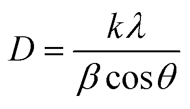
The crystallite size (D) was calculated by employing the Scherrer equation, which is expressed as,42
 | (3.1) |
The strain was determined using the formula,43
 | (3.2) |
The dislocation density which is stated as the dislocations per unit length and is given by,43
 | (3.3) |
As the annealing temperature rises to 350 °C, the microstrain (ε) as well as the dislocation density (δ) decrease, resulting in fewer lattice imperfections.44 As the annealing temperature increases to 400 °C, In2O3 bonds break instead of allowing atoms to freely move to their steady sites. This leads to the formation of stress and defects in the film. S. Pandey et al. similarly observed this behaviour in the sputtered ZnO films.45
| Γ = 4Ag + 4Eg + 14Tg + 5Au + 5Eu + 16Tu | (3.4) |
Fig. 4 shows the Raman intensity vs. wavenumber graph for indium oxide thin films that exhibit E2g mode at 130 cm−1, E1g mode at 306 cm−1, and Ag mode at 561 cm−1.47
 | ||
| Fig. 4 Raman spectra of indium oxide nanostructured films for various annealing temperatures. | ||
3.1.2.1. The E2g mode at 130 cm−1. The Raman mode at 130 cm−1 is accredited to the In–O bond in the InO6 octahedral unit and is also indicative of the crystal quality of the films.48 It is noted that the intensity of the peak is maximum for the films annealed at 350 °C, then decreases for 400 °C, suggesting that annealing at 350 °C likely facilitates sufficient grain growth and minimizes structural defects without inducing significant thermal stress. These findings, supported by X-ray diffraction (XRD) analysis, collectively indicate that annealing at 350 °C establishes the most favourable conditions for achieving superior crystal quality of the thin films.
3.1.2.2. The E1g mode at 306 cm−1. The peak at 306 cm−1 demonstrates the bending vibrations of InO6 octahedra. This mode is sensitive to oxygen vacancies.49 Since the intensity of Raman scattering is directly related to the square of the derivative of the polarizability with respect to the normal mode amplitude, a change in intensity can be anticipated upon the formation of oxygen vacancies. The highest intensity of the peak at 350 °C annealing temperature indicates the maximum amount of oxygen vacancies which is further supported by PL results.
3.1.2.3. The Ag mode at 561 cm−1. The Raman mode at 561 cm−1 demonstrates symmetric lattice vibrations of InO6 octahedra. The broadening of the Raman peak is observed for annealing temperature of 400 °C. Annealing at elevated temperatures can lead to non-stoichiometric oxygen deficiency and thermal stress, causing microstructural modifications such as grain boundary defects, cracks or strain, which contribute to the broadening of Raman peaks.50
3.1.3.1. In 3d core level spectra. Fig. 5(a) and (b) shows the core-level spectra of Gaussian-deconvoluted In2O3 thin films annealed at 300 °C and 350 °C. The spectra exhibit two characteristic In 3d components, namely In 3d5/2 and In 3d3/2. The binding energy maxima are observed at 444.1 eV and 451.7 eV, respectively, corresponding to the spin–orbit splitting of the In 3d levels. These peaks confirm the presence of trivalent indium ions (In3+) in the films. The energy separation between In 3d5/2 and In 3d3/2 is approximately 7.6 eV, which is consistent with values reported in the literature51
 | ||
| Fig. 5 High-resolution XPS spectra of In2O3 thin films: (a) In 3d core level for the film annealed at 300 °C, (b) In 3d core level for the film annealed at 350 °C, (c) O 1s core level for the film annealed at 300 °C, and (d) O 1s core level for the film annealed at 350 °C. | ||
3.1.3.2. O 1s core level spectra. The O 1s core-level spectra presented in Fig. 5(c) and (d) exhibit two well-resolved peaks, corresponding to lattice oxygen (OL) and oxygen vacancies (Ov). For the film annealed at 300 °C, the peaks are centered at binding energies of 529.59 eV and 531.13 eV, while for the film annealed at 350 °C, the peaks appear slightly shifted to lower binding energies at 529.34 eV and 530.88 eV, respectively. Quantitative analysis based on peak area fitting reveals that the proportions of lattice oxygen and oxygen vacancies are 51.23% and 48.77% for the 300 °C sample, and 51.90% and 48.10% for the 350 °C sample. Although the relative amounts of oxygen vacancies remain consistent across the two annealing conditions, the observed shift towards lower binding energies after annealing at 350 °C suggests an enhancement in the structural order of the film. Improved crystallinity and reduced defect density facilitate more efficient charge transport and suppress electron–hole recombination. Consequently, the surface becomes more chemically active and accessible, thereby enhancing the material's potential for gas sensing applications.52
3.2. Morphology of annealed In2O3 nanostructures
The thin films morphology was analysed using Field Emission Scanning Electron Microscopy (FESEM). The Fig. 6 presents FESEM descriptions of In2O3 thin films subjected to annealing at different temperatures. | ||
| Fig. 6 FESEM images of nanostructured indium oxide thin films for various annealing temperatures of (a) 250 °C, (b) 300 °C, (c) 350 °C and (d) 400 °C. | ||
The films annealed at 250 °C exhibit a smoother surface with smaller, uniformly distributed grains. Structural imperfections, such as defects or voids, are minimal at this temperature. However, with an increase in annealing temperature of 350 °C, there is a noticeable rise in defects and grain boundaries. The appearance of darker areas suggests an increase in voids and a higher concentration of oxygen vacancies. These vacancies serve as defect sites, contributing to greater porosity.53 This increase in defect density can be attributed to non-stoichiometric conditions caused by the partial loss of oxygen atoms from the lattice. The film annealed at 400 °C exhibits surface cracks, suggesting defects caused by thermal stress.54 These defects may compromise the mechanical stability of the film.
3.3. Optical studies
 | ||
| Fig. 7 Gaussian deconvoluted PL emission spectra of In2O3 nanostructures annealed at (a) 250 °C, (b) 300 °C, (c) 350 °C, and (d) 400 °C temperatures. | ||
| Annealing temperature (°C) | Parameters | UV (3.19 eV) | Violet I (3.01 eV) | Violet II (2.85 eV) | Blue I (2.68 eV) | Blue II (2.55–2.62 eV) |
|---|---|---|---|---|---|---|
| 250 | Intensity | 1232 | 2039 | 2320 | 859 | 303 |
| FWHM | 0.24 | 0.14 | 0.18 | 0.14 | 0.24 | |
| 300 | Intensity | 231 | 485 | 559 | 203 | 138 |
| FWHM | 0.22 | 0.15 | 0.16 | 0.14 | 0.33 | |
| 350 | Intensity | 940 | 1997 | 2458 | 1140 | 376 |
| FWHM | 0.24 | 0.14 | 0.16 | 0.15 | 0.24 | |
| 400 | Intensity | 1439 | 2980 | 3370 | 1187 | 657 |
| FWHM | 0.23 | 0.14 | 0.16 | 0.14 | 0.3 |
For In2O3 thin films, the photoluminescence (PL) spectra reveal emissions that can be broadly categorized into a prominent ultraviolet (UV) or near-band-edge (NBE) emission band, along with significant deep-level emissions (DLEs). The NBE emission typically corresponds to higher energy transitions near the band gap, while the DLEs arise from energies associated with defect states within the band gap. The ultraviolet emission, with an energy of 3.20 eV, is attributed to the recombination of free excitons, which may occur via exciton–exciton collisions. The near-band-edge (NBE) emission peak (3.20 eV) appeared weaker when compared to some of the peaks from deep-level emission. Such behaviour suggests that the relaxation of photoexcited carriers from the conduction band to defect states occurs more rapidly than their recombination with valence band holes.55 Saeed et al. associated the weak NBE emission with the occurrence of defects, including oxygen vacancies. They noted that a high ratio of NBE to deep-level emission is typically accredited to the quantum confinement effect. However, in this case, the contribution of quantum confinement effect to the observed photoluminescence can be ruled out.56 On the other hand, DLE bands, observed at energies of 2.57–3.02 eV, are generally linked to intrinsic point defects, including oxygen vacancies, interstitials, or antisites, within the In2O3 films.57 These visible emissions are believed to result from the recombination of deeply trapped electrons with delocalized holes in the valence band or from delocalized electrons recombining with deeply trapped holes in the conduction band. The violet-blue emission peaks observed around 3.02 eV, 2.85 eV, and 2.68 eV could be attributed to indium–oxygen vacancy centres and oxygen vacancies. The broad blue emission peak centered at 2.57 eV could be attributed to indium interstitials.58–60
Fig. 7 illustrates how annealing temperature influences the position and intensity of defect-related peaks. The peak positions remain unchanged as the annealing temperature increases, but the intensity is lowest at 300 °C. The reduction in photoluminescence (PL) intensity is attributed to a reduction in oxygen vacancies. A similar trend was reported by W. Zhong et al.,61 where the PL intensity decreased at 300 °C due to a reduction in defect density. This occurs as oxygen atoms fill the vacancies, resulting in films with improved stoichiometry. This behaviour is commonly observed in many materials, where the incorporation of oxygen reduces the density of defects, leading to diminished luminescent properties. When the annealing temperature increases from 350 °C to 400 °C, the PL intensity increases again. This can be explained by the desorption of oxygen at elevated temperatures, which creates more oxygen vacancies and defects in the film. For ITZO films, a notable increase in PL intensity was observed due to the development of non-stoichiometric conditions resulting from the loss of lattice oxygen.61 A similar trend has been reported for ZnO thin films, where higher annealing temperatures lead to an increase in defect density, thereby enhancing the PL intensity.62
No significant changes are observed in the FWHM of PL emission spectrum. This means that the nature of the emission remains the same, even though the efficiency of the emission changes.
3.4. Analysis of In2O3 nanostructures for H2S gas sensing
Studies on In2O3-based sensors have been carried out for various gases; however, the detection of H2S is particularly important due to its highly toxic and corrosive properties, even at low concentrations. The significant risks H2S poses to human health and the environment, highlight the need for precise and reliable detection, making it a crucial target for gas sensing applications. Consequently, this study is focused specifically on the detection of H2S gas.The operating temperature is a key feature in evaluating the efficiency of MOS-based gas sensors, as it significantly influences gas adsorption, desorption, and surface interactions. To identify the optimal operating temperature, In2O3 nanostructured gas sensors were tested for their response towards 4 ppm H2S across a temperature range of 150–400 °C, as illustrated in Fig. 8. The sensor response versus operating temperature studies were performed for all the sensors over three cycles to ensure reproducibility and reliability. The mean and standard deviation of the sensor responses were calculated and are presented in the Fig. 8, as well as in the ESI Table TS2.† The statistical analysis revealed that the level of significance for the observed trends is <0.05, confirming the robustness of the results.
 | ||
| Fig. 8 Operating temperature studies for nanostructured indium oxide sensors annealed at various temperatures. | ||
The results indicate that the optimum operating temperature is 250 °C. The sensors' responses to H2S steadily increase with temperature from 150 °C to 250 °C. Below 250 °C, H2S gas molecules necessitate nominal energy to surpass the threshold activation energy and interact with adsorbed oxygen species. However, above 250 °C, the responses begin to diminish. This reduction occurs because, at higher temperatures, the capacity for gas adsorption weakens, leading to rapid desorption before surface reactions can take place.63 The consistent performance across multiple cycles, supported by statistical significance, underscores the reliability of the identified optimal temperature.
The gas sensing mechanism of In2O3 towards H2S primarily operates on a chemiresistive principle, wherein the electrical resistance of the sensor varies with the concentration of the target gas.64 In2O3, being an n-type semiconductor, exhibits resistance changes due to surface redox reactions. When the sensor is exposed to air at elevated temperatures, oxygen molecules are adsorbed onto the surface and extract electrons from the conduction band of In2O3, forming chemisorbed oxygen species such as O2− and O22−. This results in the formation of an electron depletion layer at the surface, which increases the baseline resistance of the sensor. The reactions involved in oxygen chemisorption can be summarized as follows:30
| O2(g) + e− ⇌ O2−(ad) | (3.5) |
| O2−(ad) + e− ⇌ O22−(ad) | (3.6) |
Upon exposure to H2S, a reducing gas, it interacts with these chemisorbed oxygen species on the sensor surface, donating electrons back to the In2O3 conduction band. This electron release reduces the sensor's resistance and restores charge carriers, enhancing the conductivity. The primary reactions during this process are:30
| H2S(g) + e− ⇌ H2S(ad) | (3.7) |
| H2S(g) + O2x−(ad) ⇌ H2S(ad) + O2(g) + xe− | (3.8) |
| 2H2S(ad) + 3O2x−(ad) ⇌ 2SO2(g) + 2H2O + 3xe− | (3.9) |
Once the H2S flow is stopped and synthetic air is reintroduced, oxygen molecules re-adsorb onto the surface, recapturing electrons and restoring the depletion region.24 The dynamic sensing behaviour and thermal activation process are schematically illustrated in Fig. 9. Additionally, the response trends observed in Fig. 10 demonstrate that sensor performance improves with increasing H2S concentration, which can be attributed to enhanced adsorption kinetics and more effective surface reactions at higher analyte levels.65 The response and recovery parameters were calculated as detailed in the Experimental section. These findings collectively support the role of surface chemistry, oxygen vacancy dynamics, and thermally driven kinetics in enabling sensitive and selective H2S detection using In2O3 – based sensors.23
 | ||
| Fig. 9 Schematic diagram representing the H2S gas sensing mechanism for indium oxide nanostructured sensors. | ||
 | ||
| Fig. 10 Sensor response curves for In2O3 gas sensors annealed at (a) 250 °C, (b) 300 °C, (c) 350 °C, and (d) 400 °C temperatures. | ||
The data presented in ESI (TS3†) highlights the performance of the In2O3 sensors in terms of response time and recovery time at various concentrations of H2S gas and annealing temperatures, with an optimized operating temperature of 250 °C. The results clearly indicate that the response time is consistently faster than the recovery time. This phenomenon can be attributed to the faster adsorption and reduction reactions of H2S gas on the sensor surface compared to the slower desorption and oxidation reactions that occur during recovery. This trend is consistent with previous studies.66
At higher concentrations of H2S gas, the sensor exhibits quicker response times. For instance, at 4 ppm of H2S gas, the sensor annealed at 350 °C demonstrates the fastest response time of 17 ± 1 seconds. These observations are further supported by Fig. 11, which illustrates the response and recovery times as functions of H2S gas concentrations and annealing temperatures. The graph shows that the sensor annealed at 350 °C outperforms others in terms of response time while its recovery is slowest. Additionally, the graph includes error bars representing the standard deviation, which were calculated from three consecutive measurement cycles for each condition. The detailed summary of the mean values and standard deviations have been provided in ESI (Table S4†).
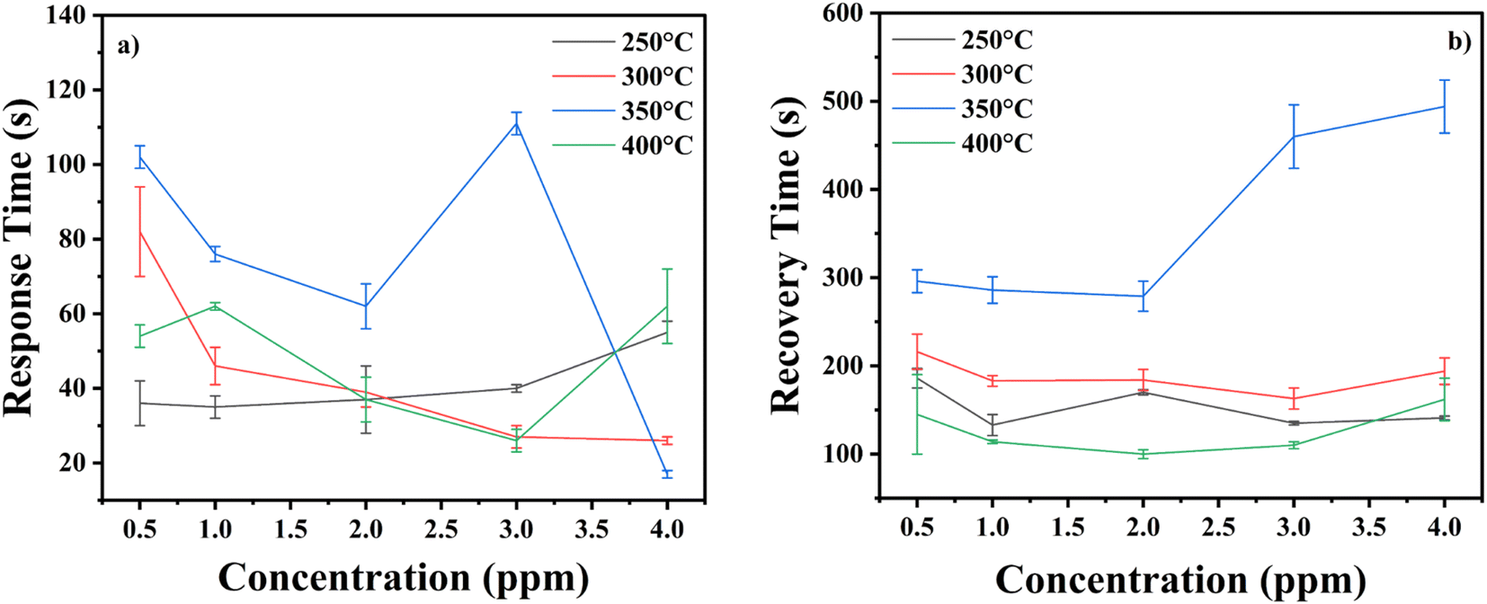 | ||
| Fig. 11 (a) Response time plots (b) recovery time plots for In2O3 sensors annealed at 250 °C, 300 °C, 350 °C and 400 °C for H2S gas. | ||
To ensure the statistical significance of the results, a level of significance (p-value) was calculated for the data. The p-value was found to be less than 0.05, indicating that the observed differences in response and recovery times, are statistically significant and not due to random variation. This reinforces the reliability of the findings and underscores the impact of annealing temperature and gas concentration on the sensor's performance.
To investigate the sensor response of the proposed H2S sensor at its optimum operating temperature, the transient sensor response was evaluated for H2S gas concentrations ranging from 0.5 to 4 ppm, as illustrated in Fig. 12. For a detailed analysis, the mean and standard deviations of the sensor response were also calculated using three consecutive measurement cycles. These standard deviations are represented as error bars in the graph providing a visual representation of the variability in the sensor response across the measurement cycles. The statistical significance of the results was also evaluated, and the p-value was found to be less than 0.05, confirming that the observed differences in sensor response are statistically significant. A comprehensive table summarizing these findings, including the mean, standard deviations, and level of significance, is provided in the ESI TS4† for further reference. The sensor annealed at 350 °C exhibited the highest sensor response value of (97.89 ± 0.08)%, highlighting its superior sensitivity at this annealing temperature. However, when the annealing temperature was increased to 400 °C, the sensor's response decreased significantly across all tested gas concentrations, suggesting that higher annealing temperatures may negatively impact the sensor's performance. Further, the results demonstrate a strong linear correlation between the sensor response and H2S concentration, with a lower limit of detection of 0.5 ppm. This indicates that the In2O3-based sensor is capable of quantitatively detecting H2S in air with high precision.
 | ||
| Fig. 12 Sensor response values for different concentrations of H2S gas. | ||
The H2S gas sensing behaviour of In2O3 thin films is influenced by various aspects, including defects, crystallinity, grain boundaries, and morphology of the films.30 As outlined in the gas sensing mechanism, oxygen vacancy (VO) defects play a pivotal role by acting as the primary adsorption sites for H2S gas, enabling effective detection.64
The oxygen-deficient materials, which provide a substantial number of contact sites, are thoroughly linked to the mechanism of gas sensing, facilitating significant changes in the electrical resistance.67 The rise in oxygen vacancy defects could be accountable for the notable improvement in the response of In2O3 thin films to the lower H2S gas concentrations. Based on the Raman and PL study, it is concluded that the sensor annealed at 350 °C has a higher concentration of oxygen vacancies compared to the other films, which aligns with its enhanced sensing response. W. Chen et al.68 reported that the increase in the number of oxygen vacancies after adding dopant provides donor states to In2O3 NBs, improves its electrical conductivity and thus, enhances its sensor response. J. Liu et al.69 demonstrated the significant role of oxygen vacancy defects in enhancing the sensitivity to H2S gas. M. Kaur et al.49 stated that the uptake and release of target gas is influenced by the interaction between bond energy of metal and oxygen, oxygen vacancies, and surface oxygen. They identified oxygen vacancies (VO) as crucial active sites for adsorption, playing a noteworthy role in the gas sensing mechanism. Although the film annealed at 400 °C exhibits the highest PL intensity, its sensing performance is not optimal. The decrease in sensor response could be due to the thermal stress and presence of cracks as confirmed from FESEM, making some active sites inaccessible for the target gas to interact. Moreover, for the films annealed at 350 °C, voids are visible from FESEM results, which may contribute to the enhanced gas sensing performance by providing higher surface area for gas adsorption. Numerous studies have highlighted the significant potential of materials with high surface area for effectively adsorbing target gas molecules.70–72
Additionally, XPS analysis further supports these findings where the shift towards lower binding energies after annealing at 350 °C suggests improved structural order, enhanced crystallinity, and reduced defect density thus facilitating more efficient charge transport, suppress electron–hole recombination, and render surface more chemically active and accessible, thereby significantly boosting the gas sensing performance.
The ability of In2O3 sensors to specifically detect H2S is critical for gas sensing applications. Selectivity, defined as the capability of sensor to differentiate a target gas with respect to other gases in a mixture, is a key parameter in this context. In this study, the sensors were evaluated against several gases, which include SO2, CO, NH3, NO2, and H2S. The selectivity data of the proposed H2S sensor is visualized in a histogram as shown in Fig. 13. The histogram provides a clear comparison of the sensor's response to H2S gas relative to other interfering gases, demonstrating its high selectivity for H2S. Error bars are included in the plot to represent the standard deviations calculated from three consecutive measurement cycles. These error bars highlight the variability in the sensor's response and further validate the consistency of its performance.
 | ||
| Fig. 13 Selectivity histogram of H2S with SO2, CO, NH3 and NO2 gases. | ||
The corresponding values for selectivity, including the mean response and standard deviations for each gas, are tabulated in TS5 of the ESI.† This table provides a detailed breakdown of the sensor's response to various gases, complementing the graphical representation in Fig. 13. Among the tested sensors, the one annealed at 350 °C demonstrated excellent selectivity for H2S, making it particularly suitable for detecting this gas.
The long-term stability of the In2O3 – based gas sensor annealed at 350 °C was evaluated after eight months of storage under ambient conditions. The dynamic response curves of the freshly fabricated and aged sensors are presented in the ESI (Fig. S3†). During the long-term measurements, the relative humidity (RH) inside the sealed gas sensing chamber was monitored using a DHT11 humidity sensor with an accuracy of ±5% RH. Initially, the RH was 73% under ambient conditions but decreased to 17% during sensor operation at 250 °C, primarily due to water desorption at elevated temperature.
A noticeable decrease in the baseline resistance of the aged sensor was observed compared to the fresh one. This change is attributed to the influence of humidity, which plays a significant role in the aging behaviour of oxide-based sensors. Over time, adsorbed water molecules interact with lattice oxygen ions in In2O3, generating free electrons and reducing baseline resistance.73 Despite this shift, the aged sensor exhibited only a slight (∼23%) decline in response to 0.5 ppm H2S gas, confirming its good long-term stability.74 Furthermore, the calculated sensor response values for both the fresh and aged sensors remained relatively consistent, indicating that the low-humidity environment during testing had minimal impact on sensor performance. These findings highlight the sensor's reliable performance over extended periods, with minor degradation likely influenced by environmental humidity and natural aging processes.
Table 3 presents a comparison of the prepared In2O3 H2S sensor along with recently reported metal oxide H2S sensors. In this work, the sensor demonstrated a remarkable response towards the lowest limit of detection (LOD) of 0.5 ppm H2S gas. Additionally, the reported In2O3 based H2S sensor exhibited good sensing performance at a concentration of 4 ppm. The findings from Raman analysis, photoluminescence spectroscopy, and FESEM analysis indicate that an increase in oxygen vacancies and surface defects confirms the influence of annealing temperature on improving H2S gas sensing response.
| Sensing material | Operating temperature (°C) | Concentration (ppm) | Sensor response | Response/recovery time (s) | References |
|---|---|---|---|---|---|
| In2O3 | 250 | 4 | 99.14% | 20/606 | Present work |
| CuO/SnO2 | 200 | 50 | 85.71% | 100/109 | 12 |
| NiO | 400 | 200 | 28.8 | 108/47 | 14 |
| In2O3 | RT | 5 | 68% | 18/507 | 66 |
| In2O3/ZnO | 250 | 50 | 44.5 | 24/27 | 71 |
| Nd2O3-loaded In2O3 | 300 | 10 | 10.11 | — | 75 |
| Ag/WO3/rGO | 150 | 100 | 685.8 | 8/38 | 76 |
4. Conclusions
In2O3 thin films were synthesized using a chemical route spin-coating method. Their properties were systematically analysed through XRD, Raman, XPS, UV-vis spectroscopy, photoluminescence, and FESEM. The sensors were tested for H2S gas sensing performance at small concentrations ranging from 0.5 to 4 ppm. Among the samples, the sensor annealed at 350 °C demonstrated a fast response time and significantly enhanced sensor response within the tested range, achieving optimal performance at an operating temperature of 250 °C. The improved sensing characteristics were primarily accredited to the existence of voids and oxygen vacancies, which facilitated gas adsorption. This study highlights the successful optimization of annealing temperature to develop In2O3 thin films for effective, and selective H2S gas detection applications. However, this study has notable limitations. One notable drawback is the relatively long recovery time observed in the sensor's performance. This delay in recovery can be attributed to the slower desorption and oxidation processes of H2S molecules from the sensor surface, which limits its efficiency in real-time applications where rapid cycling between gas exposure and recovery is essential. Addressing this limitation will be crucial for improving the practicality of the sensor in real-world scenarios.Another limitation concerns the long-term stability of the sensor. Although the sensor showed reliable performance during testing, a noticeable decrease in baseline resistance was observed in aged sensors after eight months of storage, primarily due to environmental humidity and natural aging processes. Despite this, the sensor still exhibited good stability, with only a slight (∼23%) decrease in response to 0.5 ppm H2S, indicating its robustness. However, improving the sensor's resistance to humidity and aging will be essential for extending its lifespan and enhancing its reliability in long-term applications.
To overcome the current limitations and further enhance the performance of In2O3-based H2S sensors, future studies could focus on several key areas. First, the incorporation of catalytic additives or dopants into the In2O3 matrix could be explored to accelerate the desorption process and reduce recovery time. Second, the development of hybrid nanostructures or composite materials, combining In2O3 with rGO or other metal oxides, may improve both response and recovery characteristics while maintaining high selectivity.
Data availability
The data cannot be made publicly available upon publication as they are not available in a standard format that is sufficiently accessible by other researchers. The data that support the outcomes of this study will be shared upon reasonable request from the authors.Conflicts of interest
There are no conflicts to declare.Acknowledgements
Poornesh P. would like to thank Anusandhan National Research Foundation (ANRF), Government of India for funding this work through a research project grant bearing file no. CRG/2022/007630.References
- H. Wang, J. Ma, J. Zhang and Y. Feng, J. Phys.: Condens. Matter, 2021, 33(30), 303001 CrossRef CAS.
- A. Mirzaei, S. S. Kim and H. W. Kim, J. Hazard. Mater., 2018, 357, 314–331 CrossRef CAS PubMed.
- A. Mirzaei, H. R. Ansari, M. Shahbaz, J. Y. Kim, H. W. Kim and S. S. Kim, Chemosensors, 2022, 10(7), 289 CrossRef CAS.
- A. Ahmed, A. Singh, S. J. Young, V. Gupta, M. Singh and S. Arya, Composites, Part A, 2023, 165, 107373 CrossRef CAS.
- J. Zhang, X. Liu, G. Neri and N. Pinna, Adv. Mater., 2016, 28, 795–831 CrossRef CAS PubMed.
- S. Hussain, L. Peng, J. N. O. Amu-Darko, A. Shahid, K. Yusuf, S. Wang, M. Javed Liaqat, R. K. Manavalan, X. Zhang and G. Qiao, Mater. Sci. Semicond. Process., 2024, 184, 108840 CrossRef CAS.
- Y. Liu, Y. Qi, Y. Cai, X. Bao and S. Gao, Photoacoustics, 2025, 43, 100715 CrossRef.
- S. Shao, L. Yan, L. Zhang, J. Zhang, Z. Li, H. W. Kim and S. S. Kim, ACS Appl. Mater. Interfaces, 2024, 16, 6098–6112 CrossRef CAS.
- H. Meng, Z. Liu, X. Wang and L. Feng, Environ. Sci.: Nano, 2023, 11, 459–469 RSC.
- S. G. Dasari, P. Nagaraju, V. Yelsani, S. Tirumala and M. V. Ramana Reddy, ACS Omega, 2021, 6, 17442–17454 CrossRef CAS.
- J. Y. Hu, H. Lei, H. Y. Zhang, X. X. Xue, X. P. Wang, C. H. Wang and Y. Zhang, Rare Met., 2024, 43, 6500–6515 CrossRef CAS.
- S. Ruksana, A. Kumar, S. Lakshmy, K. R. Kishore, C. S. Sharma, M. Kumar and B. Chakraborty, ACS Appl. Eng. Mater., 2024, 2, 431–442 CrossRef CAS.
- R. Jansi, M. S. Revathy, A. Vimala Juliet, M. A. Manthrammal and M. Shkir, Ceram. Int., 2024, 50(17), 29419–29427 CrossRef CAS.
- S. Srivastava, A. K. Gangwar, A. Kumar, G. Gupta and P. Singh, Mater. Res. Bull., 2023, 165, 112330 CrossRef CAS.
- X. Shi, Z. C. Lu, Q. Wang and P. Song, Vacuum, 2024, 227, 113360 CrossRef CAS.
- A. Ani, P. Poornesh, A. Antony and S. Chattopadhyay, Sens. Actuators, B, 2024, 399, 134827 CrossRef CAS.
- K. Kamlesh, D. Suthar, R. Sharma, G. Chasta, S. Panwar, H. Himanshu, L. P. Purohit and M. S. Dhaka, Phys. B, 2024, 675, 415622 CrossRef.
- Z. Jin, Y. Mou, J. Zhao, C. Chen, H. Zhou, N. Xiang, F. Wang, Z. Wang, J. Liu and L. Wu, Sens. Actuators, B, 2024, 401, 135026 CrossRef CAS.
- J. N. O. Amu-Darko, S. Hussain, M. Wang, S. Lei, A. A. Alothman, S. Mohammad, G. Qiao and G. Liu, Sens. Actuators, B, 2024, 407, 135464 CrossRef CAS.
- M. Cao, Q. Wang, J. Shang, Y. Zhou, G. Dong, L. Zhang, S. Li, Y. Cui, F. Liu and Y. Zhou, Sol. Energy Mater. Sol. Cells, 2024, 273, 112954 CrossRef CAS.
- J. Liu, Ceram. Int., 2024, 50, 24417–24424 CrossRef CAS.
- S. M. Majhi, S. T. Navale, A. Mirzaei, H. W. Kim and S. S. Kim, Inorg. Chem. Front., 2023, 3428–3467 RSC.
- S. Hussain, S. Wang, J. N. O. Amu-Darko, A. N. Begi, K. Yusuf, T. K. Ibrahim, A. Iqbal, R. K. Manavalan, X. Zhang and G. Qiao, Sens. Actuators, B, 2025, 425 DOI:10.1016/j.snb.2024.136954.
- J. Nii Okai Amu-Darko, S. Hussain, X. Zhang, A. M. Karami, M. Sufyan Javed, K. Yusuf, R. K. Manavalan, M. Wang, G. Qiao and G. Liu, Ceram. Int., 2024, 50, 38242–38252 CrossRef CAS.
- M. Kumari and M. Kumar, International Research Journal of Engineering and Technology, 2022, 9(12), 1472–1476 Search PubMed.
- N. Fellahi, M. Addou, A. Kachouane, M. El Jouad and Z. Sofiani, Eur. Phys. J.: Appl. Phys., 2016, 74(2) DOI:10.1051/epjap/2015150383.
- P. H. Ho, G. Tizzanini, S. Ghosh, W. Di, J. Shao, O. Pajalic, L. Josefsson, P. Benito, D. Creaser and L. Olsson, Energy Fuels, 2024, 38, 5407–5420 CrossRef CAS.
- A. Gurlo, N. Barsan, U. Weimar, M. Ivanovskaya, A. Taurino and P. Siciliano, Chem. Mater., 2003, 15, 4377–4383 CrossRef CAS.
- S. Chen, Y. Luo, J. Liang and Y. Pei, J. Electron. Mater., 2022, 51, 6297–6304 CrossRef CAS.
- J. Xu, X. Wang and J. Shen, Sens. Actuators, B, 2006, 115, 642–646 CrossRef CAS.
- T. Ravikumar, L. Thirumalaisamy, A. Thomas, S. Nallakumar, S. Pandiaraj, M. Mr, A. N. Alodhayb, S. Pitchaimuthu, V. Dananjaya, C. Abeykoon, K. Sivaperuman and A. N. Grace, Mater. Today Chem., 2025, 43, 102515 CrossRef CAS.
- T. Ravikumar, L. Thirumalaisamy, A. Thomas, S. Nallakumar, S. Pandiaraj, M. Mr, A. N. Alodhayb, S. Pitchaimuthu, V. Dananjaya, C. Abeykoon, K. Sivaperuman and A. N. Grace, Mater. Today Chem., 2025, 43, 102515 CrossRef CAS.
- F. Sarf, I. Karaduman Er, E. Yakar and S. Acar, J. Mater. Sci.: Mater. Electron., 2025, 36(3), 1–5 CrossRef.
- P. Gupta, K. Kumar, N. K. Pandey, B. C. Yadav and S. H. Saeed, Appl. Phys. A: Mater. Sci. Process., 2021, 127, 1–5 CrossRef.
- N. V. Srinivasa, K. Haunsbhavi, N. Srinatha, H. M. Mahesh, S. Valanarasu and B. Angadi, Mater. Sci. Eng., B, 2024, 301, 117178 CrossRef CAS.
- A. Anusha, P. Poornesh, A. Antony, I. V. Bhaghyesh, K. K. Nagaraja, S. Chattopadhyay and K. B. Vinayakumar, Sensors, 2022, 22, 2033 CrossRef CAS.
- D. R. Cox, Statistical Significance Tests, 1982, vol. 14 Search PubMed.
- M. Ghemid, H. Gueddaoui, M. Hemissi, M. R. Khelladi and R. Bourzami, Chem. Phys. Lett., 2021, 784, 139089 CrossRef CAS.
- A. Yahia, A. Attaf, H. Saidi, M. Dahnoun, C. Khelifi, A. Bouhdjer, A. Saadi and H. Ezzaouia, Surf. Interfaces, 2019, 14, 158–165 CrossRef CAS.
- I. Hotovy, J. Huran, P. Siciliano, S. Capone, L. Spiess and V. Rehacek, Sens. Actuators, B, 2001, 78, 126–132 CrossRef CAS.
- A. Bouhdjer, A. Attaf, H. Saidi, Y. Benkhetta, M. S. Aida, I. Bouhaf and A. Rhil, Optik, 2016, 127, 6329–6333 CrossRef CAS.
- V. Y. Zenou and S. Bakardjieva, Mater. Charact., 2018, 144, 287–296 CrossRef CAS.
- P. P. Prathap, G. G. Devi, Y. V. Subbaiah, K. R. Reddy and V. Ganesan, Current Applied Physics, 2008, 8(2), 120–127 CrossRef.
- V. Senthilkumar and P. Vickraman, Curr. Appl. Phys., 2010, 10, 880–885 CrossRef.
- S. K. Pandey, S. K. Pandey, V. Awasthi, A. Kumar, U. P. Deshpande, M. Gupta and S. Mukherjee, Bull. Mater. Sci., 2014, 37, 983–989 CrossRef CAS.
- M. Ghemid, H. Gueddaoui, M. Hemissi, M. R. Khelladi and R. Bourzami, Chem. Phys. Lett., 2021, 784, 139089 CrossRef CAS.
- C. Manoharan, M. Jothibas, S. J. Jeyakumar and S. Dhanapandian, Spectrochim. Acta, Part A, 2015, 145, 47–53 CrossRef CAS PubMed.
- C. Kranert, R. Schmidt-Grund and M. Grundmann, Phys. Status Solidi RRL, 2014, 8, 554–559 CrossRef CAS.
- M. Kaur, N. Jain, K. Sharma, S. Bhattacharya, M. Roy, A. K. Tyagi, S. K. Gupta and J. V. Yakhmi, Sens. Actuators, B, 2008, 133, 456–461 CrossRef CAS.
- H. Lee, B. Kim, C. Y. Gao, H. J. Choi, J. H. Ko, C. H. Seo and J. Park, Mol. Cryst. Liq. Cryst., 2019, 679, 38–47 CrossRef CAS.
- J. Liu, RSC Adv., 2015, 5(24), 18666–18672 RSC.
- G. Liu, Z. Wang, Z. Chen, S. Yang, X. Fu, R. Huang, X. Li, J. Xiong, Y. Hu and H. Gu, Sensors, 2018, 18(4) DOI:10.3390/s18040949.
- M. Vishwas, K. N. Rao, A. R. Phani, K. V. A. Gowda and R. P. S. Chakradhar, J. Mater. Sci.: Mater. Electron., 2011, 22, 1415–1419 CrossRef CAS.
- T. Özdal, T. Chtouki, H. Kavak, V. Figa, D. Guichaoua, H. Erguig, J. Mysliwiec and B. Sahraoui, J. Inorg. Organomet. Polym. Mater., 2021, 31, 89–99 CrossRef.
- D. Beena, K. J. Lethy, R. Vinodkumar, A. P. Detty, V. M. Pillai and V. Ganesan, J. Alloys Compd., 2010, 489(1), 215–223 CrossRef CAS.
- F. Saeed, A. Farooq, A. Ali, S. Mehmood, C. Cepek, S. Bhardwaj, A. Ul-Hamid and A. S. Bhatti, Mater. Sci. Eng., B, 2020, 262, 114781 CrossRef CAS.
- K. Anand, J. Kaur, R. C. Singh and R. Thangaraj, Ceram. Int., 2016, 42, 10957–10966 CrossRef CAS.
- S. C. Kulkarni and D. S. Patil, J. Mater. Sci.: Mater. Electron., 2016, 27, 3731–3735 CrossRef CAS.
- A. Yahia, A. Attaf, H. Saidi, M. Dahnoun, C. Khelifi, A. Bouhdjer, A. Saadi and H. Ezzaouia, Surf. Interfaces, 2019, 14, 158–165 CrossRef CAS.
- M. Jothibas, C. Manoharan, S. Dhanapandian and S. J. Jeyakumar, Asian J. Chem., 2013, 25, S59–S64 CrossRef CAS.
- W. Zhong, G. Li, L. Lan, B. Li and R. Chen, RSC Adv., 2018, 8, 34817–34822 RSC.
- M. Nie, Y. Zhao and Y. Zeng, J. Laser Appl., 2014, 26, 022005 CrossRef.
- K. Haunsbhavi, D. Alagarasan, N. J. Shivaramu, H. M. Mahesh, P. Murahari and B. Angadi, J. Electron. Mater., 2022, 51, 6356–6368 CrossRef CAS.
- V. Kumar, S. M. Majhi, K. H. Kim, H. W. Kim and E. E. Kwon, Chem. Eng. J., 2021, 404, 126472 CrossRef CAS.
- S. Shah, S. Hussain, S. T. U. Din, A. Shahid, J. N. O. Amu-Darko, M. Wang, Y. Tianyan, G. Liu and G. Qiao, J. Environ. Chem. Eng., 2024, 12, 112538 CrossRef CAS.
- Roopa, B. Kumar Pradhan, A. Kumar Mauraya, K. Chatterjee, P. Pal and S. Kumar Muthusamy, Appl. Surf. Sci., 2024, 678 DOI:10.1016/j.apsusc.2024.161111.
- Y. Zhang, Z. Zhang, G. Lv, Y. Zhang, J. Chen, Y. Luo and G. Duan, Sens. Actuators, B, 2024, 412, 135787 CrossRef CAS.
- W. Chen, Y. Liu, Z. Qin, Y. Wu, S. Li and P. Ai, Sensors, 2015, 15, 29950–29957 CrossRef CAS PubMed.
- J. Liu, W. Guo, F. Qu, C. Feng, C. Li, L. Zhu, J. Zhou, S. Ruan and W. Chen, Ceram. Int., 2014, 40, 6685–6689 CrossRef CAS.
- A. Mirzaei, S. S. Kim and H. W. Kim, J. Hazard. Mater., 2018, 357, 314–331 CrossRef CAS.
- J. Nii Okai Amu-Darko, S. Hussain, X. Zhang, A. M. Karami, M. Sufyan Javed, K. Yusuf, R. K. Manavalan, M. Wang, G. Qiao and G. Liu, Ceram. Int., 2024, 50, 38242–38252 CrossRef CAS.
- M. Sun, H. Yu, X. ting Dong, L. Xia and Y. Yang, J. Alloys Compd., 2020, 844, 156170 CrossRef CAS.
- H. Chai, Z. Zheng, K. Liu, J. Xu, K. Wu, Y. Luo, H. Liao, M. Debliquy and C. Zhang, IEEE Sens. J., 2022, 22(6), 5470–5481 CAS.
- K. Suematsu, N. Ma, K. Watanabe, M. Yuasa, T. Kida and K. Shimanoe, Sensors, 2018, 18(1) DOI:10.3390/s18010254.
- Z. Jin, J. Zhao, L. Liu, F. Liu, Z. Wang, F. Wang, J. Liu, Y. Mou, L. Wu and X. Wu, Sens. Actuators, B, 2024, 403, 135237 CrossRef CAS.
- Y. Gui, J. Wu, K. Tian, H. Guo, X. Qin, X. Qin, X. Guo, C. Fang and P. Liu, ACS Appl. Electron. Mater., 2023, 5, 3625–3633 CrossRef CAS.
Footnote |
| † Electronic supplementary information (ESI) available. See DOI: https://doi.org/10.1039/d5ra01394a |
| This journal is © The Royal Society of Chemistry 2025 |