
 Open Access Article
 This Open Access Article is licensed under a Creative Commons Attribution-Non Commercial 3.0 Unported Licence
Microscale image encoding on metal halide perovskite thin films for anti-counterfeiting applications
Susana Ramos-Terróna,
Gustavo de Miguela,
Dietmar Leinenbc,
Jorge Munillad and
Pablo Romero-Gómez *bc
*bc
aDepartamento de Química Física y Termodinámica Aplicada, Instituto Químico para la Energía y el Medioambiente (IQUEMA), Universidad de Córdoba, Campus de Rabanales, Edificio Marie Curie, E-14071 Córdoba, Spain
bDepartamento de Física Aplicada I, Universidad de Málaga, 29071 Málaga, Spain. E-mail: prg@uma.es
cInstituto Universitario de Materiales y Nanotecnología, IMANA, University of Malaga, Campus de Teatinos, 29071, Málaga, Spain
dDepartamento de Telecomunicaciones, Universidad de Málaga, Málaga, Spain
First published on 4th June 2025
Abstract
Metal halide perovskite thin films are a demand in many technological areas since they fulfill the requirements expected in different applications, including solar cells and LEDs. In this article, we demonstrate for the first time that perovskite thin films have the potential to be incorporated in products as an anticounterfeit solution in self-identification methods due to their ability to generate images on its surface with motifs at the microscale range. The images can be recorded using an optical microscope with a camera and can be recognized automatically using a convolutional neural network. The surface pattern of the thin films can be designed by modifying the perovskite composition, structure, and surface strain making falsification difficult to reproduce and mimic. To this end, perovskite thin films have been characterized using X-ray diffraction, UV-Vis spectroscopy and optical microscopy. We report a batch of 5 types of CsxFA1−xPbI3−xBrx perovskite thin films obtained by modifying the experimental conditions that exhibit recognized patterns with accuracy detection of 94.2%.
Introduction
Counterfeiting is a growing global problem. Specially, counterfeit goods such as medicines and high-tech products are introduced in many markets decreasing the brand reputation, the profitability of the brand, and creating sanity risks.1–8 This illegal market supposes the 5.8% of the EU imports in 2019.9 Numerous conventional anti-counterfeiting methods, such as watermarks, holograms, barcodes, and QR codes, have been developed over the past decades.10 However, many of these tags are produced using reproducible processes, making the encoded information susceptible to skilled third parties. Thus, the conventional anti-counterfeit technologies face a trade-off between security and complexity: systems that are easy to verify are usually easy to imitate or forge, and systems that are difficult to forge are usually very difficult to verify. Consequently, there is a need for anti-counterfeiting technology that overcomes these problems.Digital authentication systems with integrated circuits and blockchain-based electronic commerce are aligned with robust security frameworks used globally. However, with an estimate of more than 50 billion connected IoT devices in the market by 2030, the digital and physical worlds have become tightly integrated.11 In modern society where activities such as transportation, commerce, and the use of goods, food, and medicine are widespread, the risk of cyber-attacks is substantial.12 Consequently, alongside cybersecurity measures, physical identification has emerged as a vital anti-counterfeiting technology for goods that are distributed, traded, and consumed.
Currently, nanomaterials have been claimed as an alternative to traditional physical identification solutions that can be easily implemented in goods.13–20 Zhang et al. created diamond microparticles with SiV centers as advanced, stable, and dynamic anti-counterfeiting nanomaterials with high-capacity encoding.21 Fukuoka et al. generated invisible stealth nanobeacons, which can be used as aqueous-soluble ink for steganographic prints. These nanobeacons provide strong SERS signals that are fingerprint-like and free from pigment interference, are easily customizable for specific applications, and offer a unique technology for secure authentication and watermarking without requiring time-consuming or costly synthesis processes.22 Li et al. proposed a crypto-display which functions as both a conventional meta-hologram under single-wavelength coherent light and a reflective display under white light.23 This display uses double dielectric nanoantennas with distinct reflection spectra, allowing independent control of both modes. Under white light, it appears as a normal reflective display, but under coherent light, it reveals encrypted holographic information, making it suitable for security applications. Castaing et al. created an optical engineering of persistent luminescent nanomaterials.24 These nanotechnologies claim the creation of complex effects that are impossible to reproduce but still the technologies have the lack of not having developed a simple and objective recognition system.
Herein, we report for the first time on anticounterfeit image recognition based on surface structures formed on metal halide perovskite (MHP) thin films which can be produced by simple wet chemistry methods. Different surface patterns can be created modifying the surface strain during the material growth. The surface image is captured at the microscale by an optical microscope with a 20× objective. The images were classified using a convolutional neural network (CNN) based on deep learning architecture with supervised training.
Experimental section
Fabrication of perovskite patterned surfaces
Lead iodide (PbI2, 99%), lead bromide (PbBr2, 99%), formamidinium iodide (FAI, 98%), and cesium iodide (CsI, 99%) were sourced from Sigma-Aldrich. N,N-Dimethylformamide (DMF) 99.8% extra dry over molecular sieve, AcroSeal; dimethyl sulfoxide (DMSO) 99.7% extra dry over molecular sieve, AcroSeal; and chlorobenzene extra dry over molecular sieve, AcroSeal, were obtained from Acros Organics. Amorphous glass was supplied by Pilkington. For the cleaning process, absolute dry ethanol (maximum 0.02% water content) and isopropyl alcohol (technical grade, 99.5%) were purchased from PanReac, while Decon 90 soap was acquired from Decon. All substrates were subjected to a step-by-step cleaning procedure that included sonication in Decon 90, Milli-Q water, ethanol, and isopropyl alcohol, and concluded with a 15 minute ultraviolet-ozone treatment.Perovskite films were deposited using the antisolvent method. Cs0.17FA0.83 and Cs0.40FA0.60 perovskites were prepared from a stoichiometric solution containing CsI, FAI, PbI2, and PbBr2 in a 4![[thin space (1/6-em)]](https://www.rsc.org/images/entities/char_2009.gif) :1 mixture of DMF/DMSO. The solution was filtered through a 0.22 μm PTFE filter before spin coating. Two spin-coating protocols were followed: (1) 500 rpm for 12 seconds, followed by 3000 rpm for 30 seconds, or (2) 250 rpm for 12 seconds, followed by 1500 rpm for 20 seconds. During spin coating, chlorobenzene was dispensed 5 seconds before the end of the process to promote perovskite crystallization via the antisolvent effect. The films were subsequently annealed on a hot plate at 50 °C for 1 minute, followed by 100 °C for 30 minutes. Perovskite deposition was carried out either under ambient conditions or in an inert atmosphere (inside a glovebox).
:1 mixture of DMF/DMSO. The solution was filtered through a 0.22 μm PTFE filter before spin coating. Two spin-coating protocols were followed: (1) 500 rpm for 12 seconds, followed by 3000 rpm for 30 seconds, or (2) 250 rpm for 12 seconds, followed by 1500 rpm for 20 seconds. During spin coating, chlorobenzene was dispensed 5 seconds before the end of the process to promote perovskite crystallization via the antisolvent effect. The films were subsequently annealed on a hot plate at 50 °C for 1 minute, followed by 100 °C for 30 minutes. Perovskite deposition was carried out either under ambient conditions or in an inert atmosphere (inside a glovebox).
Thin film characterization methods and image recording
Structural characterization of the thin films by X-ray diffraction experiments were conducted on all samples using a Bruker D8 DISCOVER diffractometer, operating at 40 kV and 40 mA, with Cu Kα radiation (1.54060 Å). The measurements covered Bragg angles from 2° to 40°. The system has been used in a Bragg–Brentano configuration.UV-Vis measurements were carried out at room temperature (approximately 25 °C) using a CARY100 UV-Vis spectrometer. The measurement range spanned from 400 to 900 nm in all cases. Typical thickness of the samples used for optical characterization was around 450 nm. The absorbance spectra have been calculated as log10(1/T) where T is the transmission of thin films.
The images of thin film surfaces have been collected using a Nikon e800 optical microscope with a 20× objective and a digital camera (Nikon DXM1200).
Algorithm implementation
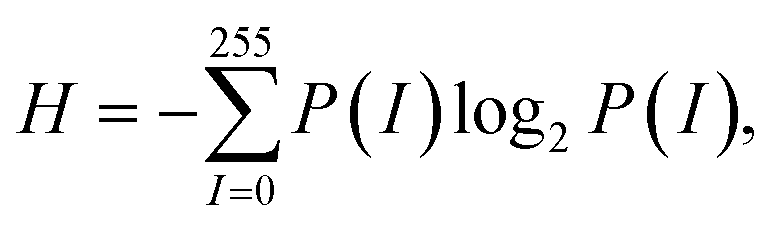
where P(I) is the probability (or frequency) of pixel intensity value, I. The possible values of entropy for a grayscale image lie within:
| 0 ≤ H ≤ 8 bits, |
 | ||
| Fig. 1 Workflow created for image classification using apas. | ||
After preprocessing, k-fold validation with k = 10 has been employed to ensure robust results. The dataset is divided into 10 disjoint groups, or folds, of samples. For each fold, the selected samples are used for testing, and the remaining samples are used for training, ensuring that each sample is used for testing exactly once. The final estimated performance is computed as the average of the results obtained across the different folds. Note that this evaluation method may underestimate the capabilities of the system, which may achieve better results with more training data by using higher values of k. However, increasing k also leads to a higher computational load, so the value k = 10 is used as a good compromise between reliable performance estimation and computational efficiency. This division is also stratified because, as shown in Fig. 2, there is a slight imbalance in the number of images across classes. For each fold, after separating the dataset into training and testing subsets, the images are further segmented into one hundred non-overlapping patches of 176 × 176 pixels. This approach increases the number of trainings samples and adjusts the input size to align with the dimensions commonly used in most classification architectures. It is important to note that this patch division is methodologically performed after the training/testing split to ensure that patches from the same image are not used simultaneously both training and testing to avoid any possibility of ‘double-dipping’. For training, data augmentation techniques, with vertical and horizontal flipping of the images across different batches, are implemented to enhance the model's generalization capabilities. As a result, the same patch may be used differently in different epochs, enhancing the robustness of the training process. Fig. 3 sketches the transformation of the images.
 | ||
| Fig. 2 Histogram of the images. | ||
 | ||
| Fig. 3 Preprocessing and transformation of optical images. | ||
Three different CNN architectures have been tested to classify the patches. CNN architectures are employed due to their ability to capture spatial hierarchies in data through convolution operations.25 Concretely, we have used the CNNs called EfficientNet developed by Google AI,26 Lenet,27 and Resnet.28 Lenet was trained completely (400k trainable parameters, with stochastic gradient descent method with learning rate 0.01 and momentum 0.9) and used as baseline, while transfer learning was employed for Resnet (77k trainable parameters, with Adam optimizer with learning rate 0.001), and fine-tunning for EfficientNet (4M tunable parameters, with Adam optimizer with learning rate 0.001). The three CNN architectures were modified to adapt their input and output layers to the patch size (176 × 176) and the number of classes (5), respectively. Additionally, the fully connected part of each network was altered so that an intermediate fully connected layer with 50 neurons precedes the final layer. This layer includes a dropout regularization layer with a factor of 0.2 and a ReLU activation layer.
For the prediction of an image's class, the outputs of these CNNs for each patch forming the image are eventually combined using a majority vote procedure. Thus, as shown in Fig. 1, this process yields two different, albeit related, types of evaluation results: one for patch classification and another for image classification.
Results and discussion
The morphology of the surface of the metal halide perovskites (MHPs) thin films is strongly dependent on the rate of film formation. Thus, modification of the relative ratio of the A-cations in the precursor solution and of deposition conditions during the spin-coating process can produce changes in the topology of the surface but also in the structure of the MHPs.29,30 XRD measurements were employed to investigate the dimensionality and structure of the formed MHPs at different experimental conditions. Fig. 4 displays the XRD patterns of the five types of MHP films prepared under different stoichiometric and deposition conditions, as summarized in Table 1. XRD patterns of the films obtained under experimental conditions 1–4 display diffraction peaks around 14.0°, 20.0°, 24.5°, 28.2° and 31.6° which can be indexed to the (100), (110), (111), (200), and (210) planes, respectively, in agreement with previously reported 3D CsxFA1−xPbI3−xBrx perovskite structures.31,32 In contrast, the film fabricated under condition 5 shows additional low-angle reflections, which are consistent with the formation of quasi-2D layered perovskite phases typically associated with increased structural anisotropy and reduced dimensionality. The position of all peaks within the experimental conditions 1 and 2 is practically invariable while it is shifted to larger 2θ values in the films prepared with the experimental conditions 3 and 4. This shift in the XRD signals is attributed to the decreased FA content in the films prepared under experimental conditions 3 and 4, which leads to unit cell contraction due to the smaller ionic radius of Cs+ compared to FA+.33 Such compositional tuning not only modifies the lattice dimensions but also induces internal lattice strain, influencing crystallinity and potentially altering the optoelectronic behavior of the films. We have also evaluated the strain (ε) for each structure by using the Williamson–Hall equation34 which relates the full-width at half-maximum (FWHM) of the XRD peaks with the crystallite size and strain of the structure.24 Our results demonstrate an increase of the strain of the MHP structure when going from experimental conditions 1 to 4 (ε = 0.128, 0.136, 0.151 and 0.190). These findings suggest that increasing the Cs+ content introduces greater lattice mismatch and mechanical stress during crystal growth, resulting in enhanced strain. This structural distortion is likely to influence defect formation and charge carrier mobility, both of which are chemically significant parameters for material performance. Regarding the film fabricated out of the glovebox (experimental condition 5) and with the same chemical stoichiometry as in 3 and 4, the XRD pattern differs considerably with respect to the other previously analyzed. Thus, the appearance of low-angle XRD peaks indicates the formation of low-dimensional MHPs, likely corresponding to quasi-2D layered perovskite phases. In these structures, FA+ cations can intercalate between inorganic [PbX6]4− octahedral slabs, leading to increased anisotropy and modified electronic properties.35 The synthesis environment (ambient vs. inert) plays a critical chemical role in directing the crystallization pathway towards these layered architectures. | ||
| Fig. 4 X-ray diffraction (XRD) patterns of the CsxFA1−xPb(Br0.17I0.83)3 MHPs films fabricated at different experimental conditions. | ||
| Sample | Composition | Spin coating two- steps | Glovebox | Perovskite type 2D or 3D | Image entropy |
|---|---|---|---|---|---|
| 1 | Cs0.17FA0.83Pb(Br0.17I0.83)3 | 500 rpm/12 s | Yes | 3D | 4.12 |
| 3000 rpm/30 s | |||||
| 2 | Cs0.17FA0.83Pb(Br0.17I0.83)3 | 250 rpm/12 s | Yes | 3D | 4.20 |
| 1500 rpm/30 s | |||||
| 3 | Cs0.40FA0.60Pb(Br0.17I0.83)3 | 500 rpm/12 s | Yes | 3D | 4.31 |
| 3000 rpm/30 s | |||||
| 4 | Cs0.40FA0.60Pb(Br0.17I0.83)3 | 250 rpm/12 s | Yes | 3D | 4.01 |
| 1500 rpm/30 s | |||||
| 5 | Cs0.40FA0.60Pb(Br0.17I0.83)3 | 250 rpm/12 s | No | 2D | 4.54 |
| 1500 rpm/30 s |
The optical properties of the MHP films are investigated by using UV-Vis absorption spectroscopy. Fig. 5 shows the absorption spectra for all films in the entire visible and near infrared region. In all films, the spectra display a broad absorption in the investigated region, as expected in MHPs. The absorption onset appears around 790 nm and 770 nm for the experimental conditions 1–2 and 3–4, respectively. The observed shift in the optical bandgap (Eb) can be directly correlated with variations in the A-site cation ratio. Cs+ incorporation into the FA-based lattice leads to structural distortions that influence the Pb–I/Br bond angles and lengths, thereby modulating the electronic band structure. Such composition-dependent bandgap engineering is a well-documented chemical strategy to tailor the optical response of halide perovskites.35 In the case of the film prepared with the experimental conditions 5, the presence of weak absorption bands around 515 nm, 565 nm and 600 nm clearly relates to the formation of low dimensional phases of the MHPs.
 | ||
| Fig. 5 UV-Vis absorption spectra of the CsxFA1−xPb(Br0.17I0.83)3 MHP films at different experimental conditions. | ||
In summary, the formation of 3D MHP films has been proven at the experimental conditions 1–4 with minor changes in the optical properties due to the different FA:Cs ratio. The crystalline structure is slightly modified due to distortions in the network introduced by the different experimental conditions.
Fig. 6 presents the optical microscopy images of the MHP thin film, illustrating various morphologies arising from the fabrication conditions outlined in Table 1. Fig. 6(1) displays a relatively uniform texture with fine surface grains, while Fig. 6(2)–(4) reveal increasing heterogeneity, suggesting compositional or structural differences. Previous studies have demonstrated that the evolution of film stress during formation plays a significant role in determining surface topography.36 Factors contributing to film stress include solvent removal, film shrinkage, phase transitions accompanied by density changes, and mismatches between the thermal expansion coefficients (CTE) of the substrate and film during annealing. Also, Janssen et al.37 and previous studies38 demonstrate the direct relation between the film stress and film strain measured by XRD. In our study, samples from 1 to 4 show a progressive increase in strain that can be correlated with the increase of surface motifs observed qualitatively on surface images. Thus, the change in the spin-coating rate and the variation in the ratio of the A-cations appears to control the morphology of the surface, although a clear correlation between all factors is beyond the scope of this work.
 | ||
| Fig. 6 Top surface images of the CsxFA1−xPb(Br0.17I0.83)3 MHP films captured using an optical microscope with a 20× objective lens. The scale bar in the image indicates a distance of 50 μm. The labelling numbers correspond to the diferent experimental conditions described in Table 1. | ||
From a chemical standpoint, the evolution of surface morphology reflects the complex interplay between ionic composition, crystallization kinetics, and interfacial strain. Changes in precursor stoichiometry alter the nucleation and growth dynamics, impacting grain size, orientation, and surface energy—factors that ultimately define the microscale texture captured in the images.
The entropy of each grayscale image was calculated individually, and the average entropy value of each class is summarized in Table 1. Across the image classes, these average entropy values range from 4.0 to 4.5. This moderate entropy level suggests that the images avoid extremes: they are neither overly simplistic, where content is easy to recognize due to low variation, nor overly chaotic, where randomness or noise obscures meaningful structures. Thus, this range indicates a balance between regions that are relatively uniform and areas with more complex textures, pointing to an adequate level of information content within the images. Images with entropy values within this range often contain patterns or structures that may not be immediately apparent to the human eye, as shown in the example of patch segmentation in Fig. 3. Thus, some portions of the images may appear featureless or uniform, while others reveal intricate details or subtle, hidden patterns.
As explained in the previous section, CNNs produce classification results for individual patches, while the classification results for entire images are determined by applying a majority vote to the patch-level results for each image. Overall classification accuracies for patches were 76%, 77% and 90% for Lenet, Resnet and EfficientNet, respectively. Table 2 summarizes the main results for these classifications providing evaluation metrics for the training patch datasets and the testing patch datasets. This is an indicator that the models are performing in a very balanced and consistent manner across the different evaluation aspects. There is no significant difference between the results for the training, and testing datasets, and also the evolution of these results across different epochs (see Fig. 7) does not appear to indicate overfitting. Finally, Table 3 collects the results for image classification after applying the majority vote. In particular, the classification accuracies increase up to 84%, 91% and 94% for Lenet, Resnet and EfficienNet, respectively. These increases are, however, lower than those expected for a majority vote if the output voters were uncorrelated. This, justifying the process followed in validation, shows a clear correlation between classifications belonging to the same image. Therefore, if a patch of an image is misclassified, the probability that other patches from the same image are also misclassified—and likely to the same incorrect class—is much higher.
| Training dataset | Testing dataset | |||||||
|---|---|---|---|---|---|---|---|---|
| CNN | Accuracy | Precision | Recall | F1-Sc | Accuracy | Precision | Recall | F1-Sc |
| Lenet | 0.9 | 0.89 | 0.89 | 0.89 | 0.76 | 0.76 | 0.8 | 0.77 |
| Resnet | 0.88 | 0.87 | 0.86 | 0.86 | 0.77 | 0.81 | 0.82 | 0.80 |
| EfficienctNet | 0.94 | 0.94 | 0.94 | 0.94 | 0.90 | 0.90 | 0.90 | 0.90 |
 | ||
| Fig. 7 Averaged learning curve for the k-folds using fine-tuning on EfficientNet. | ||
| Training dataset | Testing dataset | |||||||
|---|---|---|---|---|---|---|---|---|
| CNN | Accuracy | Precision | Recall | F1-Sc | Accuracy | Precision | Recall | F1-Sc |
| Lenet | 0.94 | 0.93 | 0.93 | 0.93 | 0.84 | 0.85 | 0.89 | 0.86 |
| Resnet | 0.97 | 0.97 | 0.96 | 0.97 | 0.91 | 0.93 | 0.94 | 0.92 |
| EfficienctNet | 0.98 | 0.98 | 0.98 | 0.98 | 0.94 | 0.94 | 0.94 | 0.94 |
EfficientNet outperforms the other two architectures. For this, Fig. 8 provides confusion matrices for the image training dataset and testing dataset. It is interesting to note that class 4 is involved in all but one misclassification, where an image of class 3 was incorrectly classified as class 1. These results may indicate that an issue with the reproducibility of some of the samples in this class may have occurred during their fabrication.
 | ||
| Fig. 8 Confusion matrices for the image training dataset (a) and testing dataset (b). | ||
Conclusions
In this study, we have presented for the first time the image classification of different batches of MHP thin films based on surface image recognition. The recognition was carried out using three different CNNs. Perovskite thin films with a CsxFA1−xPb(Br0.17I0.83)3 composition were grown via spin coating, with variations in material composition, spin coating parameters, and atmospheric control. The chemical structure, UV-visible response, and internal stress of the thin films were tailored by adjusting these conditions. XRD analysis confirmed different strain in the MHP structure depending on the film formation process. Notably, we observed the formation of both 2D and 3D perovskite thin films by modifying the growth atmosphere and chemical composition. The resulting surface images exhibited multiple patterns with an entropy value close to 4.3, highlighting the semi-hidden nature of this type of imaging. This potentially makes the images useful in contexts such as anti-counterfeiting. These images were successfully classified into five distinct categories using CNN based architectures with a 10-fold cross-validation methodology. The parallel performance trends in both the training and testing datasets indicate good convergence and minimal model overfitting. The CNN based EfficientNet architecture achieved a classification accuracy of 90% for the patches of the five image classes. These classification outputs were subsequently combined using a majority voting system, resulting in an overall image classification accuracy of 94%.Data availability
The data of the article is available at the following URL: https://drive.google.com/drive/folders/1VvUlPaGKSLDkVHRYAub9892Y_VCPFgwl?usp=sharing.Author contributions
Susana Ramos-Terrón and Gustavo de Miguel: fabrication and characterization of thin film, formal analysis, writing the technical, and discussion of the article. Pablo Romero-Gómez: idea creation, formal analysis, coordination, writing, review & editing of the article. Dietmar Leinen: formal analysis, writing and review of the article. Jorge Munilla: software generation, formal analysis, writing and review of the article.Conflicts of interest
The authors declare no conflict of interest.Acknowledgements
The authors gratefully acknowledge the financial support: PID2020-119209RB-I00 project grant funded by MCIN/AEI/10.13039/501100011033 by “ERDF A way of making Europe”. Funding for open access charge: Universidad de Málaga/CBUA. This research was supported by the BIOSIP Research Group (TIC-251), and partly funded by the project PID2022-138933OB-I00: ATQUE, funded by MCIN/AEI/10.13039/501100011033/FEDER, EU.References
- J. Deng, et al., Multiplexed Anticounterfeiting Meta-image Displays with Single-Sized Nanostructures, Nano Lett., 2020, 20, 1830–1838 CrossRef CAS PubMed
.
- R. Pittiglio, Counterfeiting and firm survival. Do international trade activities matter?, Int. Bus. Rev., 2023, 32, 102145 CrossRef
- J. Sun, X. Zhang and Q. Zhu, Counterfeiters in Online Marketplaces: Stealing Your Sales or Sharing Your Costs, J. Retail., 2020, 96, 189–202 CrossRef
- W. Ren, G. Lin, C. Clarke, J. Zhou and D. Jin, Optical Nanomaterials and Enabling Technologies for High-Security-Level Anticounterfeiting, Adv. Mater., 2020, 32, 1901430 CrossRef CAS
- X. Yu, H. Zhang and J. Yu, Luminescence anti-counterfeiting: from elementary to advanced, Aggregate, 2021, 2, 20–34, DOI:10.1002/agt2.15
- R. Arppe and T. J. Sørensen, Physical unclonable functions generated through chemical methods for anti-counterfeiting, Nat. Rev. Chem., 2017, 1, 0031 CrossRef CAS
- Y. Zhong, Q. Wang and G. Chen, Controllable preparation of carboxymethyl cellulose/LaF3:Eu3+ composites and its application in anti-counterfeiting, Int. J. Biol. Macromol., 2020, 164, 2224–2231 CrossRef CAS PubMed
- J. Jeong, et al., Unveiling the origin of performance reduction in perovskite solar cells with TiO2 electron transport layer: conduction band minimum mismatches and chemical interactions at buried interface, Appl. Surf. Sci., 2019, 495, 143490 CrossRef CAS
- Global Trade in Fakes, OECD, 2021, DOI:10.1787/74c81154-en.
- V. Maritano, et al., Anticounterfeiting and Fraud Mitigation Solutions for High-value Food Products, J. Food Prot., 2024, 87, 100251 CrossRef CAS PubMed
- P. Nguyen, et al., Advances in Secure IoT Data Sharing, Foundations and Trends® in Privacy and Security, 2024, vol. 7, pp. 1–73 Search PubMed
- O. Niki, G. Saira, S. Arvind and D. Mike, Cyber-attacks are a permanent and substantial threat to health systems: education must reflect that, Digital Health, 2022, 8 DOI:10.1177/20552076221104665
- M. S. Hasanin, et al., Sustainable multifunctional zinc oxide quantum dots-aided double-layers security paper sheets, Heliyon, 2023, 9, e14695 CrossRef CAS
- V. Sharma, et al., Nanoparticles as fingermark sensors, TrAC, Trends Anal. Chem., 2021, 143, 116378 CrossRef CAS
- A. M. Abdelaziz, et al., Protective role of zinc oxide nanoparticles based hydrogel against wilt disease of pepper plant, Biocatal. Agric. Biotechnol., 2021, 35, 102083 CrossRef CAS
- W. Han, et al., Ultraviolet emissive Ti3C2Tx MXene quantum dots for multiple anti-counterfeiting, Appl. Surf. Sci., 2022, 595, 153563 CrossRef CAS
- S. Singh, et al., Biodegradable cellulose nanocrystal composites doped with carbon dots for packaging and anticounterfeiting applications, Nanoscale, 2025, 17, 904–918 RSC
- J. M. Kim, et al., Background color dependent photonic multilayer films for anti-counterfeiting labeling, Nanoscale, 2022, 14, 5377–5383 RSC
- N. H. Minh, K. Kim, D. H. Kang, Y. E. Yoo and J. S. Yoon, Anti-counterfeiting labels of photonic crystals with versatile structural colors, Nanoscale Adv., 2024, 6, 5853–5860 RSC
- D. Li, et al., Anti-counterfeiting SERS security labels derived from silver nanoparticles and aryl diazonium salts, Nanoscale Adv., 2022, 4, 5037–5043 RSC
- T. Zhang, et al., Multimodal dynamic and unclonable anti-counterfeiting using robust diamond microparticles on heterogeneous substrate, Nat. Commun., 2023, 14, 2507 CrossRef CAS PubMed
- T. Fukuoka, et al., Physically unclonable functions taggant for universal steganographic prints, Sci. Rep., 2022, 12, 985 CrossRef CAS
- J. Li, Y. Chen, Y. Hu, H. Duan and N. Liu, Magnesium-Based Metasurfaces for Dual-Function Switching between Dynamic Holography and Dynamic Color Display, ACS Nano, 2020, 14, 7892–7898 CrossRef CAS PubMed
- V. Castaing, M. Romero, J. Torres, G. Lozano and H. Míguez, Scattering Spheres Boost Afterglow: A Mie Glass Approach to Go Beyond the Limits Set by Persistent Phosphor Composition, Adv. Opt. Mater., 2024, 12, 2301565 CrossRef CAS
- X. Zhao, et al., A review of convolutional neural networks in computer vision, Artif. Intell. Rev., 2024, 57, 99 CrossRef
- M. Tan and Q. V. Le, EfficientNet: Rethinking Model Scaling for Convolutional Neural Networks, Proc. 36th Int. Conf. Mach. Learn. (ICML), 2019, 97, 6105–6114 Search PubMed
- Y. LeCun, L. Bottou, Y. Bengio and P. Haffner, Gradient-Based Learning Applied to Document Recognition, Proc. IEEE, 1998, 86(11), 2278–2324, DOI:10.1109/5.726791
- K. He, X. Zhang, S. Ren and J. Sun, Deep Residual Learning for Image Recognition, in Proceedings of the IEEE Conference on Computer Vision and Pattern Recognition (CVPR), 2016, pp. 770–778, DOI:10.1109/CVPR.2016.90
- R. Guo, et al., Strain-Release [2π + 2σ] Cycloadditions for the Synthesis of Bicyclo[2.1.1]hexanes Initiated by Energy Transfer, J. Am. Chem. Soc., 2022, 144, 7988–7994 CrossRef CAS
- A. D. Taylor, et al., A general approach to high-efficiency perovskite solar cells by any antisolvent, Nat. Commun., 2021, 12, 1878 CrossRef CAS
- A. D. Jodlowski, A. Yépez, R. Luque, L. Camacho and G. de Miguel, Benign-by-Design Solventless Mechanochemical Synthesis of Three-, Two-, and One-Dimensional Hybrid Perovskites, Angew. Chem., 2016, 128, 15196–15201 CrossRef
- S. Ramos-Terrón, J. F. Illanes, D. Bohoyo-Gil, L. Camacho and G. de Miguel, Insight into the Role of Guanidinium and Cesium in Triple Cation Lead Halide Perovskites, Sol. RRL, 2021, 5, 2100586 CrossRef
- S. Ramos-Terrón, L. Camacho, J.-P. Correa-Baena, C.A.R. Perini and G. de Miguel, Chelating diamine surface modifier enhances performance and stability of lead halide perovskite solar cells, Mater. Today, 2025, 85, 60–68 CrossRef
- A. D. Jodlowski, et al., Large guanidinium cation mixed with methylammonium in lead iodide perovskites for 19% efficient solar cells, Nat. Energy, 2017, 2, 972–979 CrossRef CAS
- C. C. Boyd, R. Cheacharoen, T. Leijtens and M. D. McGehee, Understanding Degradation Mechanisms and Improving Stability of Perovskite Photovoltaics, Chem. Rev., 2019, 119, 3418–3451 CrossRef CAS
- K. A. Bush, et al., Controlling Thin-Film Stress and Wrinkling during Perovskite Film Formation, ACS Energy Lett., 2018, 3, 1225–1232 CrossRef CAS
- G. C. A. M. Janssen, Stress and strain in polycrystalline thin films, Thin Solid Films, 2007, 515, 6654–6664 CrossRef CAS
- U. Welzel, J. Ligot, P. Lamparter, A. C. Vermeulen and E. J. Mittemeijer, Stress analysis of polycrystalline thin films and surface regions by X-ray diffraction, J. Appl. Crystallogr., 2005, 38, 1–29 CrossRef
| This journal is © The Royal Society of Chemistry 2025 |