
 Open Access Article
 This Open Access Article is licensed under a Creative Commons Attribution-Non Commercial 3.0 Unported Licence
Control of electrical properties in solution-processed ATO thin-film transistors through gallium doping
Bu Kyeong Hwang†
,
Ji Hyang An†,
Bo Ram Lee,
Eun Jin Park,
Hyunsung Jung,
Min-Kyu Son ,
Hyeon Jin Jung* and
Soo Won Heo*
,
Hyeon Jin Jung* and
Soo Won Heo*
Nano Convergence Materials Center, Korea Institute of Ceramic Engineering and Technology (KICET), Jinju 52851, Republic of Korea. E-mail: soowon.heo@kicet.re.kr
First published on 28th April 2025
Abstract
In this study, we investigated the effects of Gallium (Ga) doping on the electrical properties of solution-processed Antimony-Tin Oxide (ATO) thin-film transistors (TFTs). Notably, ATO films initially exhibited no switching characteristics due to their high conductivity. However, doping Ga into ATO successfully induced switching behavior. The Antimony–Gallium–Tin Oxide (AGTO) TFT, with a Ga doping concentration of 20%, demonstrated excellent electrical performance, achieving a saturation mobility of 1.12 cm2 V−1 s−1 and an on/off current ratio of 4.68 × 10⁴. Furthermore, the device exhibited stability under both negative and positive bias stress conditions, with threshold voltage shifts of −2 V and +1.8 V, respectively. These results are attributed to the introduction of Ga, which not only reduced the electron concentration by creating holes within the Tin oxide matrix but also decreased oxygen-related defects in the film due to the strong bonding affinity of Ga with oxygen. Additionally, Ga doping suppressed crystallization in the ATO film, thereby contributing to the formation of highly uniform films. Consequently, it was demonstrated that AGTO allows effective control over defects and carrier concentration by adjusting the Ga content. Therefore, solution-processed AGTO is anticipated to be a promising oxide semiconductor for low-cost and large-area applications.
Introduction
Metal oxide-based thin-film transistors (TFTs) exhibit high optical transparency due to their wide optical bandgap. Additionally, they demonstrate excellent electrical properties, such as high on/off current ratios and mobility. The capability for solution processing further enables cost-effective fabrication, positioning metal oxide TFTs as a key technology for next-generation display applications.1,2 To date, various oxide TFTs incorporating materials such as Indium–Zinc Oxide (IZO),3 Indium–Gallium–Zinc Oxide (IGZO),4 Indium–Tin Oxide (ITO),5 and Indium–Gallium–Tin Oxide (IGTO)6,7 have been extensively studied. However, achieving high mobility and stability remains a persistent challenge in the field of oxide TFTs, prompting ongoing research into new compositions.Antimony-Tin Oxide (ATO) has attracted attention due to its excellent electrical properties, adequate transparency in the visible spectrum, and compatibility with low-cost processing methods. These characteristics make it suitable for various applications, including flat-panel devices and smart windows.8 Within ATO, Sb2O5 acts as a donor, generating electron carriers and enhancing the conductivity of tin oxide (SnO2) films.9 These electrons, located at donor energy levels, are easily excited to the conduction band, contributing to the high electron mobility of ATO. However, despite these advantages, ATO has not been investigated for TFT applications due to its high carrier concentration exceeding approximately 1021 cm−3.10,11
To achieve superior switching characteristics, the carrier concentration of oxide semiconductor channel layers generally needs to be below 1017 cm−3.12 Carrier concentration can be controlled by adjusting the film thickness or by doping with cations that have high metal–oxygen (M–O) bond strength, thereby reducing oxygen vacancies (Vo).6,13 In metal oxides, Vo acts as a donor, contributing to carrier concentration by providing two free electrons due to oxygen loss (Vo → Vo2+ + 2e−).14
Qi Li et al. explored the control of carrier concentration in ITO films by varying their thickness.15 They reported that increasing the ITO film thickness from 6 nm to 9 nm led to an increase in Vo content, which acted as shallow donors, thereby enhancing mobility and shifting the threshold voltage (Vth) negatively. However, as the ITO films were fabricated using sputtering, achieving precise nm-level thickness control in solution-processed films remains challenging. Recently, most works with high carrier concentration materials use vacuum process due to decrease in the on–off ratio and poor reliability.13,16,17 Although thin films fabricated by vacuum processes exhibit high quality, they also have drawbacks such as process complexity, long fabrication times, and high costs. Therefore, studies on solution processes that have advantages such as low cost and simplicity is necessary.
In solution-processed oxide TFTs, various carrier suppressors, including Hafnium,18 Zirconium,19 Magnesium,20 Yttrium,21 and Gallium (Ga),6 have been investigated for controlling carrier concentration. Since the groundbreaking report on IGZO by Hosono's group in 2004,4 Ga has been actively studied due to its high M–O dissociation energy (285 kJ mol−1), which promotes M–O bonding and effectively suppresses Vo. This defect control enhances both the performance and stability of TFTs while reducing electron trapping in the films.
Zhang et al. investigated the effects of co-doping Sb and Ga into SnO2.22 They reported that Ga3+ ions substituted Sn4+ ions, generating holes that recombined with electrons, thereby reducing the electron carrier concentration. However, the behavior of SnO2 co-doped with Sb and Ga in applications such as TFTs has not been reported.
In this study, we fabricated solution processed ATO TFTs by doping Ga, a carrier suppressor, into ATO at varying concentrations (10%, 20%, and 30%). The introduction of Ga effectively controlled the carrier concentration in ATO thin films. Notably, adding Ga dopants to highly conductive ATO thin films without switching characteristics resulted in Antimony–Gallium–Tin Oxide (AGTO) (Ga: 20%) TFTs with an on/off ratio of approximately 105. Furthermore, AGTO (Ga: 20%) TFTs exhibited excellent stability under negative bias stress (NBS) and positive bias stress (PBS) conditions, with Vth shifts of −4.8 V and +4.6 V, respectively. These results indicate that Ga effectively suppressed Vo, which contributes to high carrier concentrations and defect states.
Interestingly, as the Ga doping concentration increased, the subthreshold swing (S.S.) improved, suggesting that Ga doping reduced impurities such as OH-bonding. This study demonstrates that Ga is an effective dopant for reducing defects in ATO channel layers.
Experimental
Synthesis of metal oxide solution
Antimony(III) chloride (SbCl3), Tin chloride hydrates (SnCl4·xH2O), and gallium nitrate hydrates (Ga(NO3)3·xH2O) were dissolved separately in 2-methoxyethanol. The ATO solution was synthesized with a total concentration of 0.3 M, with Sb/Sn ratios of 0.05. The AGTO solution was prepared by adding varying amounts of Ga as a dopant to the ATO solution. The mixture solutions were stirred with a magnetic bar for 2 h at 700 rpm and 80 °C.Device fabrication
The TFTs fabrication process is shown in Fig. 1(a). The substrates used in this study were SiO2/Si substrates consisting of a heavily p-type doped Si wafer with a 100 nm-thick SiO2 layer grown via wet oxidation. The Si layer served as the gate, and the SiO2 layer acted as the gate insulator. The substrates were cleaned sequentially in deionized water, detergent, acetone, and isopropyl alcohol using an ultrasonic cleaner, with each step lasting 10 minutes. After cleaning, the substrates were dried on a hot plate at 150 °C for 10 minutes.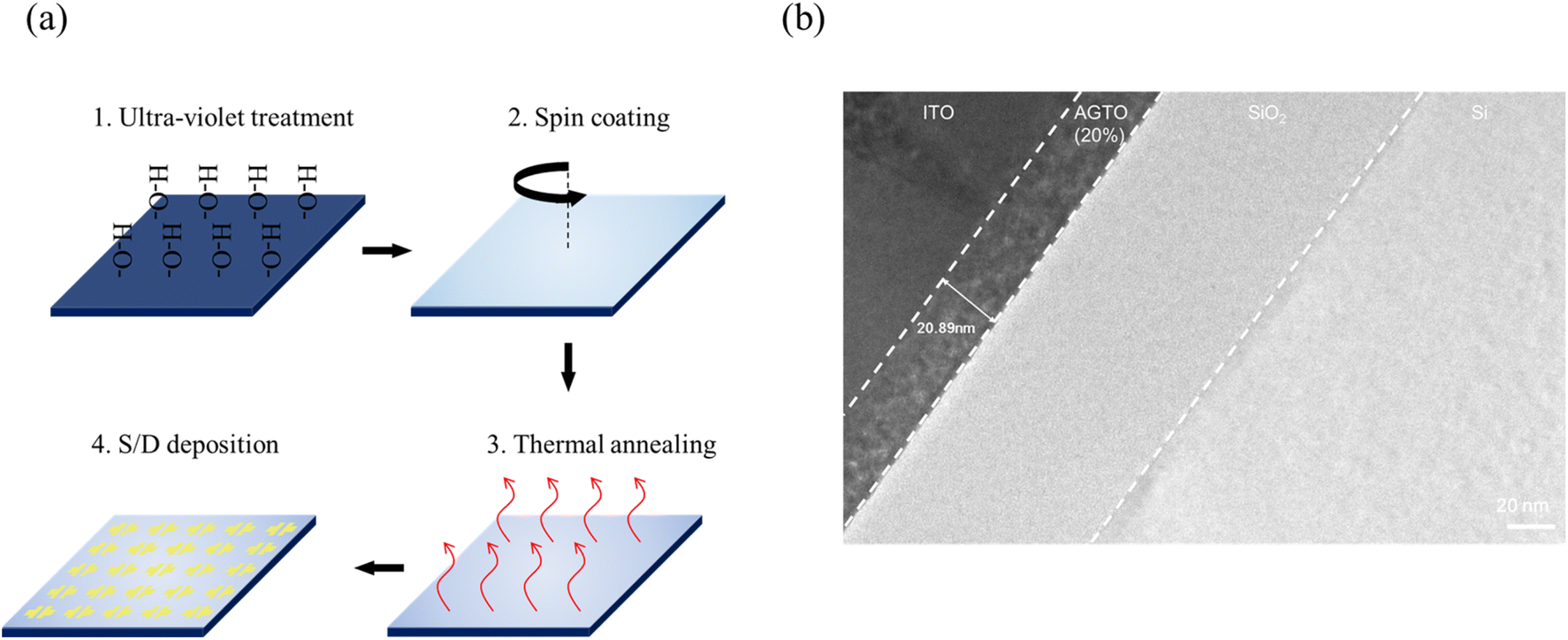 | ||
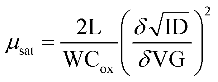
| Fig. 1 (a) Experimental procedures of AGTO films and TFTs, (b) cross-sectional TEM image of AGTO(Ga20%) TFT. | ||
Prior to coating the active layer, the substrates were irradiated in an ultraviolet ozone cleaner (AC-16, Ahtech) for 10 minutes to remove organic residues and enhance adhesion. ATO and AGTO thin films were spin-coated at 5000 rpm for 20 seconds and subsequently pre-annealed on a hot plate for 10 minutes. All devices underwent thermal annealing at 550 °C for 1 hour in an ambient air environment.
The source/drain electrodes were fabricated by depositing a 100 nm-thick ITO film via magnetron sputtering, followed by patterning through a lift-off process. The active channel width and length were designed to target 400 μm and 100 μm, respectively, for characterizing the electrical properties of the ATO and AGTO devices.
Fig. 1(b) shows the cross-sectional TEM image of AGTO(Ga: 20%) TFT at the ITO/AGTO(Ga20%)/SiO2/Si region. It can be confirmed that the AGTO(Ga: 20%) TFT has a well-defined layer without defect structures at the gate/gate insulator/semiconductor interfaces.
Device characterization
The electrical characteristics and bias stress tests of the fabricated TFTs were measured using an HP 4145B semiconductor parameter analyzer (Hewlett Packard) under ambient air and dark conditions. The transfer curves were obtained by sweeping the gate voltage (VGS) from −40 V to 40 V in 0.5 V increments. The chemical compositions of the ATO and AGTO thin films were analyzed using an X-ray photoelectron spectrometer (XPS) equipped with an Al Kα (1486.68 eV) source (NEXSA XPS, Thermo Fisher Scientific). The binding energy was calibrated to 284.5 eV using the C 1s peak.The crystallinity and amorphous state of the films were evaluated using a grazing incidence X-ray diffractometer (GI-XRD) (D8 Advance A25 Plus) with an incident angle of 1°, measured over the 2θ range of 10° to 80°.
Results and discussion
Fig. 2(a) illustrates the structure of the fabricated AGTO TFT, while Fig. 2(b) shows the transfer curves used to compare the electrical characteristics of the AGTO TFTs. The ATO TFT does not exhibit switching characteristics due to the high and constant drain current, which may be attributed to its high electrical conductivity. In contrast, switching characteristics are observed in AGTO TFTs starting from a Ga doping ratio of 10%. Notably, as the Ga doping ratio increases, the off current decreases, indicating that the excessive carriers are effectively reduced by Ga doping. Fig. 2(c) presents the variation in the electrical parameters of AGTO TFTs as a function of the Ga doping ratio, as extracted from the transfer curves. These values are summarized in Table 1. The mobility was calculated using the equation:and Vth was determined by extrapolating IDS1/2. The AGTO (Ga: 10%) TFT exhibits Vth of −15.5 V, operating in the on state without the application of a positive voltage. However, due to its relatively high off current compared to the on current, the on/off ratio is low at 9.20 × 10². By increasing the Ga ratio, the AGTO (Ga: 20%) TFT demonstrates Vth of 1.5 V, allowing it to operate in the off state without applying a negative voltage. Its mobility increases approximately threefold to 1.12 cm2 V−1 s−1 compared to AGTO (Ga: 10%) TFT, and the on/off ratio improves significantly to 6.68 × 10⁴, representing a 72-fold increase. This improvement results from a substantial reduction in off current while maintaining a similar on current compared to AGTO (Ga: 10%). Ga doping introduces Ga3+ ions, replacing Sn4+ ions, and generates holes in the film.20 These generated holes form electron–hole pairs with the existing electrons, reducing the electron carrier concentration and thereby contributing to the reduced off current.
 | ||
| Fig. 2 (a) Schematic illustration of the bottom-gate top-contact AGTO TFT. (b) Transfer characteristics of the ATO and AGTO TFTs with various Ga ratio (VDS = 20.1 V). (c) Electrical characteristics (mobility, Vth, and S.S.) of the AGTO TFTs with various Ga ratio. (d) Carrier concentration of the AGTO TFTs with various Ga ratio. | ||
| Mobility (cm2 V−1 s−1) | Vth (V) | S.S·(V per decade) | On/off ratio | Dit (cm−2 eV−1) | |
|---|---|---|---|---|---|
| ATO | — | ||||
| AGTO (Ga: 10%) | 0.42 | −15.5 | 20.13 | 9.20 × 10² | 7.50 × 10¹³ |
| AGTO (Ga: 20%) | 1.12 | 1.5 | 3.77 | 6.68 × 10⁴ | 1.39 × 10¹³ |
| AGTO (Ga: 30%) | 0.06 | 16.5 | 2.18 | 1.31 × 10⁴ | 7.93 × 10¹² |
Fig. 2(d) shows the carrier concentration of the AGTO TFTs. As the Ga concentrations increased, the carrier concentration decreased. The carrier concentration of the AGTO (Ga: 30%) film could not be measured due to its high electrical resistivity. These results support the above explanation of the Ga doping mechanism.
However, the AGTO (Ga: 30%) TFT shows a mobility of only 0.06 cm2 V−1 s−1, representing a 95% decrease compared to AGTO (Ga: 20%), and the Vth shifts positively to 16.5 V. These results indicate that while Ga doping suppresses excessive carrier generation and reduces the off current, excessive doping degrades the electrical performance of the TFTs. Therefore, the Ga doping level must be carefully optimized to avoid deterioration of electrical properties.
Interestingly, although the mobility of AGTO (Ga: 30%) TFT decreased, the S.S. improved to 2.18 V per decade, representing a 43% improvement compared to AGTO (Ga: 20%) TFT (3.77 V per decade). This improvement can be attributed to a reduction in impurities due to the promotion of M–O bonding by Ga doping. Impurities within the film can act as defects between the channel layer and gate insulator, causing electron scattering. Improved switching performance is directly linked to a reduction in interface trap density (Dit), confirming the effectiveness of Ga doping in reducing defects.
The specific mechanisms behind the reduction in Dit will be further discussed in the XPS analysis section.
The S.S. of AGTO TFTs exhibiting switching characteristics was calculated using the equation:

The Dit was derived using the following equation:

Table 2 shows the electrical properties of the reported the carrier suppressor doping oxide TFTs. The comparison shows that AGTO can effectively suppress the carrier and achieve a small Vth. It exhibits that AGTO can be an advantageous material for low-power applications such as mobile displays and flexible electronics.
To investigate the effects of Ga concentration on the chemical bonding states of AGTO films, XPS analysis was conducted. Fig. 3(a)–(d) show the O 1s and Sb 3d spectra of ATO and AGTO films with varying Ga doping ratios, and the results are summarized in Fig. 3(e). The O 1s peak was deconvoluted into three components OI (530.4 eV ± 0.1), OII (531.6 eV ± 0.1), and OIII (532.0 eV ± 0.1) using Gaussian fitting.26 OI corresponds to oxygen in the lattice, OII represents Vo, and OIII is associated with impurities such as metal hydroxyl bonding (OH-bonding). The Sb 3d peaks were fitted at 529.8 eV ± 0.1 and 539.7 eV, corresponding to Sb 3d5/2 and Sb 3d3/2, respectively.
 | ||
| Fig. 3 XPS spectra of ATO and AGTO films with various Ga concentrations: O 1s peaks for the chemical bonding states of the (a) ATO film, AGTO films with (b) Ga: 10%, (c) Ga: 20% and (d) Ga: 30%, respectively. (e) Content evolution of OI, OII, and OIII as a function of the Ga ratios. (f) Ga 2p peak. (g) Sn 3d peak. | ||
For the ATO film, the relative concentrations of OI, OII, and OIII were 32.4%, 34.8%, and 29.3%, respectively. In comparison, the AGTO (Ga: 10%) film showed a 52% increase in OI to 49.3%, while OII and OIII decreased to 34% and 12.8%, respectively, representing reductions of 2% and 57% compared to the ATO film. These results indicate that Ga doping promotes M–O bonding while reducing defects such as Vo and OH-bonding. Interestingly, the OII peak exhibited a smaller decrease (2%) compared to OIII. Since Vo contributes to carrier concentration by supplying electrons in oxide semiconductors, its limited reduction may explain the high off current observed in the AGTO (Ga: 10%) TFT in Fig. 2(b).
For AGTO (Ga: 20%), the OI component increased by 6% to 52.5%, while OII and OIII decreased by 7% and 15%, respectively, compared to AGTO (Ga: 10%). This aligns with the observed reduction in off current and improvement in S.S. for AGTO (Ga: 20%) TFT in Fig. 2(b). Additionally, Vo induces electron scattering, which impacts electrical properties.27 The reduction in Vo likely contributed to decreased electron trapping, thereby facilitating carrier transport and enhancing mobility.
In AGTO (Ga: 30%), the OI peak increased to 67.7%, while OII and OIII decreased to 19.8% and 7.6%, respectively. Notably, the OII peak showed a 38% reduction compared to AGTO (Ga: 20%), which can be attributed to the excessive reduction in carrier concentration caused by over-doping with Ga. This result supports the significant degradation in electrical performance observed in AGTO (Ga: 30%) TFT, such as a tenfold decrease in mobility and a Vth shift exceeding 15 V, as shown in Fig. 2(b).
As mentioned earlier, the improved Dit of AGTO (Ga: 30%) TFT is closely associated with the reduction in OIII. Impurities such as OH-bonding cause trapping at the interface, impairing switching characteristics.28 Consequently, Ga doping effectively reduces impurities in the film, and the decreasing trend of OIII correlates well with the improvement in Dit.
Fig. 3(f) displays the Ga 2p spectra for ATO, AGTO (Ga: 10%), AGTO (Ga: 20%), and AGTO (Ga: 30%) films. The central peaks of Ga 2p3/2 and Ga 2p1/2 were located at binding energies of 1117–1118 eV and 1144–1145 eV, respectively. As the Ga content increased, these peaks shifted slightly to higher binding energies, suggesting an increase in the oxidation state of Ga–O bonds. This observation aligns with the trend of increasing M–O bonding with higher Ga content, as shown in Fig. 3(e).29
Fig. 3(g) presents the Sn 3d spectra of AGTO films with various Ga concentrations. As the concentration of Ga increased, Sn 3d binding energy shifted to lower binding energies. It indicates that the substitution of Sn4+ by Ga3+ upon Ga doping, as the lower charge state of Ga3+ reduces the binding energy of Sn.
To evaluate the crystallinity of ATO and AGTO films with varying Ga concentrations (10%, 20%, and 30%), GI-XRD analysis was performed. Fig. 4 shows the GI-XRD patterns of films annealed at 550 °C after spin coating. The diffraction peaks of the ATO film match those of tetragonal SnO2 (JCPDS No. 41-1445). This indicates that Sb is incorporated into the SnO2 lattice by substituting Sn ions without forming new compounds, consistent with the findings reported in ref. 30. The ATO film exhibits a polycrystalline structure with diffraction planes corresponding to (110), (101), (211), (200), and (220).
 | ||
| Fig. 4 GI-XRD patterns of ATO film, AGTO films with various Ga concentrations. | ||
In contrast, as the Ga content increases, the intensity of the diffraction peaks gradually weakens, and the peaks broaden. This indicates that the incorporation of Ga induces a reduction in grain size of films, which correlates with the decreasing trend of Dit presented in Table 1. Interestingly, no shifts in the diffraction peaks were observed, suggesting that Ga substitution does not induce significant structural changes. These results confirm that Ga doping introduces lattice distortions in SnO2, leading to progressive amorphization. As the ionic radius of Ga3+ (0.71 Å) is smaller than that of Sn4+ (0.71 Å), the lattice distortion can be confirmed to result from different charge balance and ionic radius between Ga3+ and Sn4+. Notably, the crystallinity of AGTO (Ga: 30%) was significantly diminished, approaching an amorphous state.
Le et al. demonstrated a similar amorphization trend in cadmium (Cd) oxide TFT devices, where increasing Ga content caused broadening and disordering of Cd peaks in GI-XRD patterns. At a Ga content of 30% (Cd![[thin space (1/6-em)]](https://www.rsc.org/images/entities/char_2009.gif) :Ga = 7:3), the peaks became broad and disordered.31 Additionally, Lingjiao et al. reported that by adjusting the Ga doping level in solution-processed Gallium–Tin Oxide (GTO) TFTs, the films transitioned from polycrystalline to amorphous. When the Ga content exceeded 40%, the GI-XRD spectra showed no discernible peaks.32 These findings align with the results observed in this study, indicating that ATO films undergo amorphization with increasing Ga doping.
:Ga = 7:3), the peaks became broad and disordered.31 Additionally, Lingjiao et al. reported that by adjusting the Ga doping level in solution-processed Gallium–Tin Oxide (GTO) TFTs, the films transitioned from polycrystalline to amorphous. When the Ga content exceeded 40%, the GI-XRD spectra showed no discernible peaks.32 These findings align with the results observed in this study, indicating that ATO films undergo amorphization with increasing Ga doping.
Since TFTs are applied to display backplanes, their reliability under external stress is a critical factor. In particular, VGS stability is essential for ensuring the proper operation of TFTs in display applications. Fig. 5 shows the results of bias stress tests conducted to evaluate the stability of TFTs under gate bias conditions. Fig. 5(a)–(d) depict the results of the NBS test and PBS test, negative bias illumination stress (NBIS) test and positive bias illumination stress (PBIS) test, respectively. For these tests, VGS of ±10 V was applied, and transfer curves were measured at 100, 500, 1000, 5000, and 10000 seconds. The illumination stress was set to 1000 lux of light source. The AGTO (Ga: 20%) TFT exhibited excellent stability, with a Vth shift of −4.8 V under NBS and a positive shift of 4.6 V under PBS. In addition, a Vth shift of the AGTO (Ga: 20%) TFT under NBIS and PBIS was −9.8 V and +8.6 V, respectively.
 | ||
| Fig. 5 (a) Negative bias stress, (b) positive bias stress, (c) negative bias illumination stress, (d) positive bias illumination stress test for AGTO (Ga: 20%) TFT. | ||
Oxide TFTs without a passivation layer are known to be highly susceptible to environmental factors, such as oxygen and moisture in the air. Specifically, under negative bias, the reaction H2O(g) + H+ ↔ H2O+(s) causes moisture from the atmosphere to be adsorbed onto the back channel. Conversely, under positive bias, the reaction O2(g) + e− ↔ O2−(s) leads to oxygen adsorption, resulting in a positive shift in Vth. These shifts are also closely related to interface trap sites.
In particular, under the NBIS stress, Vo is ionized due to light, generating more electrons in the conduction band. It causes a large Vth shift in the negative direction. In addition, under the PBIS, the electrons are trapped in the trap state, inducing a positive Vth shift. When bias stress is applied, charges in the active layer become trapped at the interface between the channel and gate insulator, causing significant Vth shifts. However, the AGTO (Ga: 20%) TFT demonstrated improved stability due to the reduction of defects such as Vo and OH-bonding, achieved through Ga doping. This reduction contributed to the enhancement of device reliability under various conditions.
Conclusion
In this study, we successfully induced switching characteristics in highly conductive ATO by doping it with Ga using a solution-process. The electrical properties, chemical bonding states, and crystalline structures of ATO and AGTO films with various Ga/(Sb + Sn) ratios (0%, 10%, 20%, 30%) were analyzed using I–V curves, XPS, and GI-XRD. The transfer curves confirmed that excessive charge carriers in ATO were suppressed by Ga doping, enabling the control of switching characteristics. As the Ga doping content increased, the Vth shifted positively, attributed to a reduction in Vo formation due to the high dissociation energy of Ga–O bonds. This result is consistent with the XPS analysis, which showed a decrease in Vo proportion with increasing Ga doping. These findings demonstrate that Ga acts as a controller to suppress excessive carrier generation by reducing Vo. Notably, the AGTO (Ga: 20%) TFT exhibited outstanding electrical performance, including a mobility of 1.12 cm2 V−1 s−1, Vth of 1.5 V, and an on/off ratio of 6.68 × 10⁴. Furthermore, under PBS (VGS = 10 V, VDS = 20.1 V) and NBS (VGS = −10 V, VDS = 20.1 V) the Vth shifts were minimal (+4.6 V and −4.8 V, respectively) after 10000 seconds. These results confirm that AGTO is a viable candidate for use as an active layer in TFTs. In conclusion, we developed a novel composition, AGTO, and demonstrated its potential application as an active layer in TFTs. Consequently, AGTO is expected to become a promising candidate material for transparent electronic devices through further research and development.
Data availability
All data is available within the manuscript.Conflicts of interest
There are no conflicts to declare.Acknowledgements
This research was supported by the National Research Foundation of Korea (NRF) funded by the Ministry of Science and ICT (NRF-2020M3H4A3081867) and funded by the Ministry of Trade, Industry and Energy (MOTIE) (RS-2024-00418877).References
- W. Xu, H. Li, J.-B. Xu and L. Wang, ACS Appl. Mater. Interfaces, 2018, 10, 25878–25901 CrossRef CAS PubMed.
- R. Chen and L. Lan, Nanotechnology, 2019, 30, 312001 CrossRef CAS PubMed.
- H.-L. Zhao, G. Tarsoly, F. Shan, X.-L. Wang, F.-Y. Lee, Y. J. Jeong and S.-J. Kim, Sci. Rep., 2022, 12, 19497 CrossRef CAS PubMed.
- K. Nomura, H. Ohta, A. Takagi, T. Kamiya, M. Hirano and H. Hosono, Nature, 2004, 432, 488–492 Search PubMed.
- H. S. Kim, M.-G. Kim, Y.-G. Ha, M. G. Kanatzidis, T. J. Marks and A. Facchetti, J. Am. Cem. Soc., 2009, 131, 10826–10827 CrossRef CAS PubMed.
- Y. Wang, Z. Wang, K. Huang, X. Liang, C. Liu, C. Chen and C. Liu, Appl. Phys. Lett., 2020, 116, 141604 CrossRef CAS.
- H. Kim, S. Maeng, S. Lee and J. Kim, ACS Appl. Electron. Mater., 2021, 3, 1199–1210 Search PubMed.
- A. R. Babar, S. S. Shinde, A. V. Moholkar, C. H. Bhosale, J. H. Kim and K. Y. Rajpure, J. Alloys Compd., 2010, 505, 416–422 CrossRef CAS.
- M. Sun, J. Liu and B. Dong, Curr. Appl. Phys., 2020, 20, 462–469 Search PubMed.
- L. Liu, M. Ueda and T. Kawaharamura, RSC Adv., 2023, 13, 13456–13462 RSC.
- S. D. Ponja, B. A. D. Williamson, S. Sathasivam, D. O. Scanlon, I. P. Parkin and C. J. Carmalt, J. Mater. Chem. C, 2018, 6, 7257–7266 RSC.
- J.-S. Park, J. K. Jeong, Y.-G. Mo, H. D. Kim and G.-J. Kim, Appl. Phys. Lett., 2008, 93, 033513 CrossRef.
- C.-Y. Park, S.-P. Jeon, J. B. Park, H.-B. Park, D.-h. Kim, S. H. Yang, G. Kim, J.-W. Jo, M. S. Oh, M. Kim, Y.-H. Kim and S. K. Park, Ceram. Int., 2023, 49, 5905–5914 CrossRef CAS.
- Y.-Y. Chen, Y. Liu, L. Wang, B. Li, X.-M. Xiong and R. Chen, IEEE J. Electron Devices Soc., 2021, 9, 2168–6734 Search PubMed.
- Q. Li, J. Dong, D. Han and Y. Wang, Membranes, 2021, 11, 929 CrossRef CAS PubMed.
- L. Ji, X. Chen, X. Su, J. Wan, Z. Tu, H. Wu and C. Liu, Appl. Phys. Lett., 2023, 122, 202105 CrossRef CAS.
- L. Guo, Q. Wang, C. Wang, X. Chu, Y. Hao, Y. Chi and X. Yang, Micromachines, 2024, 15, 1445 CrossRef PubMed.
- W. Li, C. Gao, X. Li, J. Yang, J. Zhang and J. Chu, Microelectron. Eng., 2024, 286, 112142 CrossRef CAS.
- Z. Deng, Z. Liang, H. Ning, Y. Yang, X. Fu, M. Li, S. Jin, B. Jiang, R. Yao and J. Peng, J. Alloys Compd., 2024, 1008, 176778 CrossRef CAS.
- W.-Y. Lee, H. Lee, S. Ha, C. Lee, J.-H. Bae, I.-M. Kang, K. Kim and J. Jang, Elecronics, 2020, 9, 523 CAS.
- D. Afouxenidis, N. R. Halcovitch, W. I. Milne, A. Nathan and G. Adamopoulos, Adv. Electron. Mater., 2020, 6, 1900976 CrossRef CAS.
- S. Zhang, H. Zhang, S. Leng, Y. Leng, Y. Wen, H. Wang and Z. Li, J. Mater. Sci.: Mater. Electron., 2022, 33, 23821–23833 CrossRef CAS.
- J. Cao, D. Liu, W. Xia, F. Liu and B. Chen, IEEE J. Electron Devices Soc., 2023, 11, 406–410 CAS.
- F. Jaehnike, D. V. Pham, C. Bock and U. Kunze, J. Mater. Chem. C, 2019, 7, 7627–7635 RSC.
- J.-H. Na, J.-H. Park, W. Park, J. Feng, J.-S. Eun, J. Lee, S.-H. Lee, J. Jang, I. M. Kang, D.-K. Kim and J.-H. Bae, Nanomaterials, 2024, 14, 466 CrossRef CAS PubMed.
- H. J. Kim, S. Y. Je, J. Y. Won, J. H. Baek and J. K. Jeong, Phys. Status Solidi RRL, 2014, 8, 924–927 CrossRef CAS.
- X. Li, H. Zhang, X. Lu, Z. Fang, R. Yao, Y. Wang, H. Tao, H. Liang, H. Ning and J. Peng, Superlattices Microstruct., 2020, 137, 106317 CrossRef CAS.
- W. Park, J.-H. Park, J.-S. Eun, J. Lee, J.-H. Na, S.-H. Lee, J. Jang, I. M. Kang, D.-K. Kim and J.-H. Bae, Nanomaterials, 2023, 13, 2231 CrossRef CAS PubMed.
- T.-C. Li, C.-F. Han, T.-H. Kuan and J.-F. Lin, Opt. Mater. Express, 2016, 6, 343–366 CrossRef CAS.
- R. Ramanathan, S. Nagarajan, S. Sathiyamoorthy, B. Manavaimaran, H. C. Barchilia and R. C. Mallik, Mater. Adv., 2024, 5, 293–305 RSC.
- M. N. Le, P. Lee, S.-H. Kang, K. Ahn, S. K. Park, J. Heo and M.-G. Kim, J. Mater. Chem. C, 2023, 11, 7433–7440 RSC.
- L. Zhang, D. Zhu, S. Han, Y. Lu, M. Fang, W. Liu, P. Cao and W. Xu, Ceram. Int., 2020, 46, 19557–19563 CrossRef CAS.
Footnote |
| † Bu Kyeong Hwang and Ji Hyang An contributed to the work equally as joint first authors. |
| This journal is © The Royal Society of Chemistry 2025 |