
 Open Access Article
 This Open Access Article is licensed under a Creative Commons Attribution-Non Commercial 3.0 Unported Licence
One-step flashlight processing of MOF thin films for non-linear light absorption†
Nikolaj A.
Zhestkij
*a,
Svyatoslav A.
Povarov
 a,
Lev
Volodin
b,
Rostislav
Chelmodeev
b,
Mikhail
Melkomukov
b,
Yuliya
Kenzhebayeva
a,
Sergey S.
Rzhevskiy
a,
Sergei A.
Shipilovskikh
a,
Anastasia V.
Lubimova
a,
Maria V.
Timofeeva
a and
Valentin A.
Milichko
*c
a,
Lev
Volodin
b,
Rostislav
Chelmodeev
b,
Mikhail
Melkomukov
b,
Yuliya
Kenzhebayeva
a,
Sergey S.
Rzhevskiy
a,
Sergei A.
Shipilovskikh
a,
Anastasia V.
Lubimova
a,
Maria V.
Timofeeva
a and
Valentin A.
Milichko
*c
aSchool of Physics and Engineering, ITMO University, St. Petersburg, 197101, Russia. E-mail: nikolaj.zhestkij@metalab.ifmo.ru
bFaculty of Power Engineering, Bauman Moscow State Technical University, Moscow, 105005, Russia
cInstitut Jean Lamour, Universite de Lorraine, UMR CNRS 7198, 54011 Nancy, France. E-mail: valentin.milichko@univ-lorraine.fr
First published on 14th March 2025
Abstract
Although flashlight processing is an energy-efficient and fast technological approach for one-step patterning of polymers, metals, and dielectrics for diverse applications, it has not yet been implemented for hybrid materials such as metal–organic frameworks (MOFs). Herein, we report a one-step and large-scale patterning of different MOF thin films using a flash xenon lamp and a given mask in real time with cm2 s−1 speed. Structural and morphological analyses confirmed that the resulting patterns consisted of carbon and metal derivatives. We demonstrated that the resulting patterns acted as visible and near-infrared light absorbers with nonlinear absorption coefficients of 102 to 104 cm GW−1, exceeding those of most of the metal films, initial MOFs, and metal–carbon hybrids. Thus, these results open up a universal one-step approach to pattern arbitrary MOFs for nonlinear optical applications in desired ways.
Introduction
Metal–organic frameworks (MOFs), composed of inorganic and organic building blocks linked together via coordination bonds, possess tunable porosity and composition.1,2 These have made MOFs promising materials for gas separation/sorption, catalysis, and energy applications.3–6 Followed by the conventional synthetic approaches to fabricate MOFs7 for diverse applications, their patterning (by post-processing or structuring) endows them with new functionalities. For instance, the self-assembly of MOF particles,8,9 MOF patterning,10 shaping,11 pyrolysis, and scaling from nanocrystal to thin-film (TF) forms12 enable tuning the sorption and catalytic properties and extending the optical and electronic applications. Moreover, MOF patterning provides simple integration with optoelectronic devices.13,14 For optical and electronic applications, patterns greatly influence nonlinear optics and the corresponding planar/microscale devices as the hybrid structure of MOFs provides efficient modulation, nonlinear absorption, and high conversion of light.15–21Laser processing21–24 and lithography25–27 are considered as scalable and industry-oriented approaches to pattern MOFs. They make it possible to pattern the MOFs (and other materials)28–30 to create planar components for optics, electronics, medicine, and sensors. However, despite their high level of scalability and pattern resolution (up to 50 nm for MOFs),25 these approaches are still energy-consuming and require relatively long patterning times (with rare exceptions).28–30
Herein, we report a one-step process to pattern MOF TFs through flashlight. Although flashlight approach has been proven as an energy-efficient and fast technological approach to pattern polymers, metals, and dielectrics,31 it has not yet been implemented for hybrid materials such as MOFs. Using a flash xenon lamp and a given mask, we developed arbitrary images on different MOF TFs in real time with cm2 s−1 speed in this study. Structural and morphological analyses confirmed that the resulting patterns consisted of carbon and metal derivatives. We also demonstrated that the resulting patterns acted as visible and near-infrared light absorbers: Z-scan technique revealed that patterns of varying thicknesses demonstrated the saturation absorption process with up to 104 cm GW−1 nonlinear coefficient, which exceeded the values of most of the metal films, initial MOFs, and metal–carbon hybrids. Thus, these results open up a universal one-step approach for fast and large-scale optical patterning of arbitrary MOFs for nonlinear optics in desired ways.
Results and discussion
As model MOFs, we selected HKUST-1,32 consisting of Cu ions, coordinated together with a 1,3,5-benzenetricarboxylate (BTC) ligand, its bimetallic forms (containing Cu–Ni, Cu–Co, and Cu–Fe ions),33 and ZIF-8 (see ESI†). A relatively simple process of nucleation and growth of these MOFs34 makes them suitable for TF deposition.35 In this work, 220–280 °C decomposition temperature36 of HKUST-1 should simplify the flashlight processing and reduce the energy consumption. As a result, the decomposition of HKUST-1 and ZIF-8 MOFs (depending on the environmental conditions)36 generally provides carbon, metal, and metal oxide derivatives.21,37Initial TFs of HKUST-1 were deposited by a spin-coating method (see Experimental section and Video S1 (ESI†); for its bimetallic forms and ZIF-8, see the ESI†). In detail, two automated microfluidic pumps were filled with a solution of Cu(NO3)2 and BTC in ethanol (1.5 mmol and 3 mmol per 100 mL of ethanol, respectively), releasing up to 700 drops of solution one by one onto Menzel glass, mounted on a rotating and heated holder (300 rpm, 100 °C, see Video S1, ESI†). This spin-coating setup have allowed us to fabricate MOF TFs recently with a surface roughness up to 200 nm.38 The structure of obtained HKUST-1 TFs was confirmed by powder X-ray diffraction (PXRD, Fig. S1, ESI†), elemental analysis (Fig. S2 and S3, ESI†), and Raman analysis (Fig. 3b), while the thickness of the TFs (app. 30 μm) was determined by scanning electron microscopy (SEM). The structure of initial bimetallic HKUSTs and ZIF-8 TFs was also confirmed by PXRD, elemental, and Raman analyses (Fig. S9, S10, S12, and S14, ESI†).
Then, we performed flashlight processing of the TFs (see Experimental section and Video S2, ESI†). For this, each TF was mounted under a light source (pulsed xenon lamp, Fig. 1A) at a distance of 2 cm, while 0.5 mm-thick brass mask of the desired pattern was placed on the top of the TF. The obtained patterns (logo and variable width stripes, Fig. 1B–H) on HKUST-1 TF can be characterized by a metallic shine. It should also be noted that the spatial resolution (with up to 70 μm, Fig. S21, ESI†) and the quality of the flashlight patterning in Fig. 1A are limited by white light diffraction at the aperture,39 heat transfer, and the geometry of the mask itself (smoothed boundaries of the patterns appeared, when the width of the aperture is less than the mask thickness). Concerning the contribution of heat transfer, the transition from isolators (such as glass) to heat-conducting surfaces can reduce the gradient of the pattern boundary (Fig. S21, ESI†), thereby additionally improving the spatial resolution.
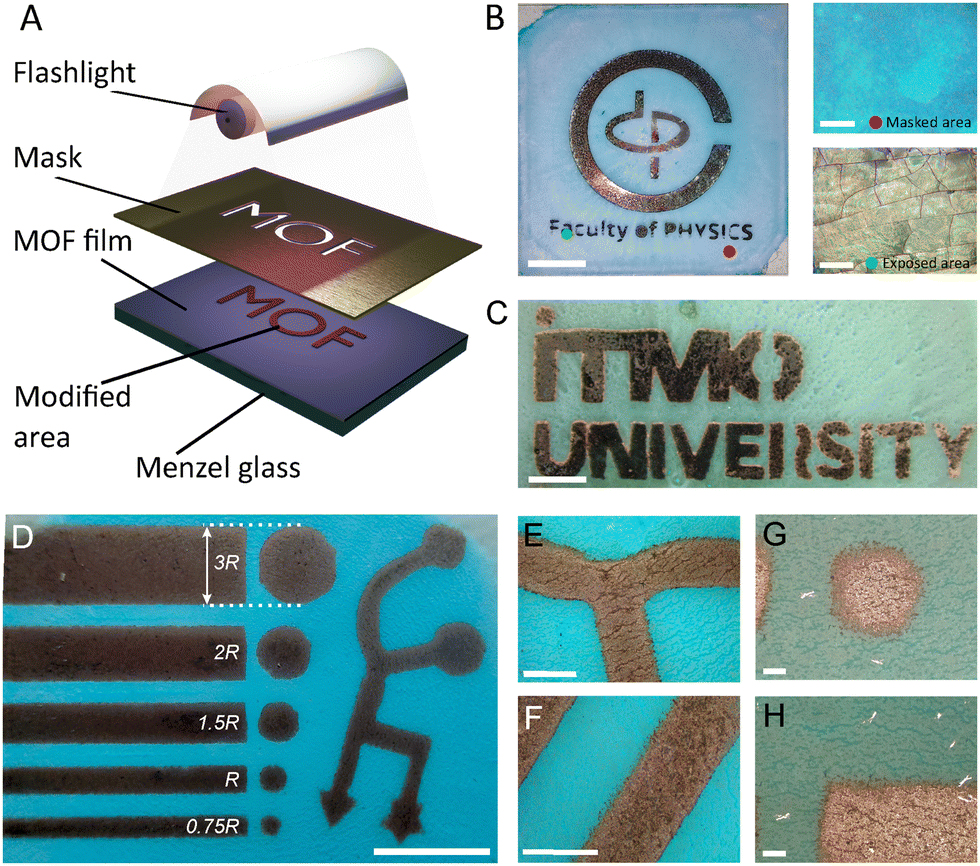 | ||
| Fig. 1 (A) Scheme of flashlight processing of MOF TF (Video S2, ESI†). (B) Pattern on HKUST-1 TF after a series of 10 pulses with a surface energy density of 2.7 J cm−2, and the optical images of the characteristic masked (upper image) and exposed (lower image) areas. Scale bars = 1 cm (left), 250 μm (right). (C) Optical image of the pattern obtained after a series of 50 pulses with a surface energy density of 1.8 J cm−2. Scale bar = 500 μm. (D) Optical image of the arbitrary pattern with the fixed size of elements (R = 1 mm). Scale bar = 500 μm. (E)–(H) Magnified optical images of an arbitrary pattern from (D). Scale bars = 1 mm (E) and (F) and 200 μm (G) and (H). | ||
The comparison of the optical properties of initial HKUST-1 TF and its pattern (Fig. 2) revealed that the flashlight process caused radical changes in both transmission (2-fold decrease of transmission for the pattern, Fig. 2A) and reflection spectra. Here, the latter is similar to the spectrum of light reflection from pure copper (Fig. 2B).
 | ||
| Fig. 2 (A) Transmittance and (B) reflectance spectra for the initial (black curve) and patterned (red curve) HKUST-1 TF. | ||
In a series of test experiments with HKUST-1 TF of a fixed thickness (app. 30 μm), we discovered the threshold values of the surface energy of flashlight, required to initiate the patterning. At the surface energy values less than 1.5 J cm−2, no changes of HKUST-1 TF could be observed, regardless of the number of the flashlight pulses. However, we detected the characteristic changes (i.e., the appearance of a metallic sheen) when operating at 1.8 J cm−2 even at a single flashlight pulse. An increase in the number of the flashlight pulses (irradiation dose) did not lead to additional changes in this case. However, the thickness inhomogeneities of the initial HKUST-1 TF resulted in different degrees of patterning by a single flashlight pulse (three distinguished areas in Fig. 3A). Using a confocal Raman spectrometer in the non-destructive mode (see the Experimental section), we analysed these areas (Fig. 3A): The first unmodified area of HKUST-1 TF did not absorb enough energy to initiate the visual changes (Fig. 3B, red curve correlating well with the Raman spectrum of initial HKUST-1).21 The second area demonstrated the metallic shine, probably associated with broken coordination bonds and partial diffusion/nucleation of Cu.40 Indeed, Raman spectra revealed the decreased intensity of the coordination bond peak (270 cm−1),21 and the appearance of halo in the region of 1200–1700 cm−1 (Fig. 3B, green curve), which indirectly confirmed the amorphization (Fig. S5, ESI†) and carbonization41 of MOFs. The third area in Fig. 3A corresponds to a complete MOF decomposition, characterized by the vanished Raman vibration of organic ligands, coordination bond breaking,21 and appearance of carbon Raman peaks (Fig. 3B, black curve).41 Elemental analysis (Fig. S2–S7, ESI†) also confirmed the carbonization and appearance of Cu after flashlight patterning of HKUST-1 TF. Herein, the morphological analysis of the patterns (Fig. 4A) revealed the heterogeneity of the surface of the patterned TF with a well-defined macroscale granular structure (partially detached from the surface due to the thermal stresses, Fig. 4B). The cross-section SEM micrographs determined the thickness of the patterned area varying from 0.1 to 2 μm (Fig. 4D and Fig. S4, ESI†), while the elemental analysis along the pattern (Fig. 4H–K) revealed a decrease in carbon (due to the thinning of the pattern itself and partial evaporation of carbon). Nevertheless, the patterned area still contained carbon (Fig. 3B) and agglomerated Cu-based particles (Fig. 4F–G and Fig. S6, S7, ESI†). Similar results were obtained for the patterned bimetallic HKUST-1 and ZIF-8 (Fig. S11 and S13, ESI†).
 | ||
| Fig. 3 (A) Characteristic stages of the patterning of HKUST-1 TF by single pulse and a set of pulses (C) at a fixed surface energy of 1.8 J cm−2 with the corresponding Raman spectra (B). | ||
 | ||
| Fig. 4 SEM micrographs and elemental analysis of the patterned area of HKUST-1 TF: (A) top view, (B) angled view and (C) and (D) cross-section view. Scale bars = 200 μm, 100 μm, 200 μm and 2.5 μm, respectively. (E) Top-view SEM micrograph of the exposed area. Scale bar = 10 μm. (F) SEM micrograph and (G) the corresponding EDS map of Cu particle agglomerates. Scale bar = 2 μm. (H) EDS scan of carbon distribution across the exposed line. (I) SEM micrograph and the corresponding EDS map of (J) carbon and (K) copper distribution on the exposed and unexposed areas of HKUST-1 TF. Scale bar = 500 μm. | ||
The transition from a single flashlight pulse mode to a set of pulses at a fixed surface energy of 1.8 J cm−2 is shown in Fig. 3C. It can be observed that the first pulse led to a local change in Fig. 3A, corresponding to the appearance of carbon (black area) and Cu (responsible for the metallic shine). Then, subsequent pulses only increase the probability of absorption of their energy and expand the surface of patterned area of the TF. This process repeats until the whole TF becomes completely patterned and the flashlight pulses does not cause any changes.
It is important that the number of pulses (30 pulses with 1.8 J cm−2 in our case), needed for the complete patterning of the TF, depends on the pulse energy (above the threshold) and the TF thickness, which determine the level of absorbed light. Thus, the flashlight patterning can be considered as adaptive and tunable through TF thickness and the number/energy of the flashlight pulses.
We should also mention that at a high level of pulse energy for patterning, the surface roughness and crystalline orientations of MOF TFs vanished its significance. Thus, the flashlight patterning can be applicable for diverse MOF TFs (with different thermal stabilities) obtained by spin coating (HKUST-1 and ZIF-8, Fig. S12, ESI†) and other methods (for example, dripping of bimetallic HKUST-1, Fig. S8, ESI†). Despite the increased thickness of bimetallic HKUST-1 TFs (up to 0.2 mm), the flashlight patterning (at 1.4 to 7 Hz repetition rate, 30 pulses) during 30 s was also successful (Fig. S11 and Fig. S20, ESI†).
In accordance with the capabilities of the flashlight approach,31 the pulse repetition rate can be increased up to 30 Hz, thereby reducing the patterning time. The latter is important for the transition of the Lab approach to industry: the laser processing and lithography of various materials25–30 and MOFs (Table 1 and Table S3, ESI†)42–50 scale from cm2 h−1 to cm2 s−1 speed, while we reached the desired patterning speed up to cm2 s−1 (see Video S2, ESI†). The next feature of the Lab approach is spatial resolution (70 μm in our case, Fig. S21, ESI†): In contrast to laser processing and lithography of MOFs,21–26 demonstrating up to 50 nm resolution (Table 1 and Table S3, ESI†), the flashlight is limited by the white light diffraction at the aperture39 and heat transfer process, and can potentially reach several hundred nanometers.48
| Approach | Source | Resolution | Speed/Exposure time | MOF | Product of patterning | Substrate | Ref. |
|---|---|---|---|---|---|---|---|
| Laser metallurgy | Pulsed fiber laser (1064 nm central wavelength, 20 kHz pulse repetition rate, 80–100 ns pulse duration) | 55–380 μm | 15 mm2 s−1 | MOFs based on Fe, Co, Ni, Zn, Cd, In, Pb and Bi | Metal nanoparticles covered with graphene shell | Glass | 23 |
| 70 mm s−1 | Ce-MOF | CeO2 nanoclusters with Pt nanoparticles | 42 | ||||
| Laser ablation | Pulsed Femto-, pico- and nano-second lasers | HKUST-1, ZIF-8, ZIF-67, UiO-66 | Carbon, metal and metal oxide nanocrystals, MOF nanocrystals, amorphous MOF | 21 | |||
| Laser nanoforging | Pulsed fiber laser (1064 nm central wavelength, 1–10 Hz pulse repetition rate, 5 ns pulse duration) | 150 nm | ZIF-8 | ZIF-8 thin film | Metal foil, PET | 43 | |
| Laser carbonization | Pulsed CO2 laser (10.6 μm central wavelength, 9–10 W integral power) | 150 μm | ZiF-67 (Co) | Porous graphene | LIMDG polyamide | 44 | |
| CO2 laser (10.6 μm central wavelength, 2.4–7.8 W integral power) | 80–270 mm s−1 | Fe (MIL), Ni-BDC, HKUST-1 | Metal nanoparticles with an amorphous carbon | Metal foil, carbon paper, carbon cloth | 45 | ||
| CaN laser diode (450 nm central wavelength, 5.5 W integral power) | 50 μm | ZiF-67 (Co) | Co/N doped amorphous carbon | 46 | |||
| Laser interference patterning | Continuous diode laser (532 nm central wavelength, 40 mW integral power) | 5 μm | HKUST-1 | Copper oxide and amorphous carbon | Glass | 47 | |
| Nonlinear lithography | Femtosecond laser (850–1300 nm wavelength, 150 fs pulse duration, 1 MHz pulse repetition rate) | 400 nm | 150 fs, and 30–120 s | Er-BTC | Amorphous area inside a crystal volume | MOF crystal on Menzel glass | 48 |
| Femtosecond laser (780 nm central wavelength, 80 MHz pulse repetition rate, 100 fs pulse duration) | 700-800 nm | 250 ms | MOF-5 | Metallic patterns inside a crystal volume | 49 | ||
| UV-lithography | Hg lamp | min | ZIF-8 | Etched ZIF-8 | Glass, Si, Au, Ag, Pt, Pd | 50 | |
| Flashlight | Pulsed Xe lamp | 70–120 μm | 140 μs/cm2 s−1 | HKUST-1, bimetallic HKUST-1 (Cu–Co, Cu–Ni, Cu–Co), ZIF-8 | Metal oxide nanoparticle agglomerations with an amorphous carbon | Glass | This work |
Concerning the application,21–23 the large-scale MOF derivatives and patterns possess diverse functionalities from catalysis to energy and optics. This is due to the presence of metal open sites, residual porosity, and carbon nature. It is important that this set can additionally provide efficient absorption of light over a wide spectral range for nonlinear light absorbers17,18 and coatings. To prove this, we performed Z-scan measurements with an open aperture for the patterns on HKUST-1, bimetallic, and ZIF-8 TFs (see the Experimental section and ESI†).51 For this, Thorlabs AC lenses were used to build a telescope system at wavelengths of 1030 nm (254-50-AB-ML) and 515 nm (Mitutoyo NIR 10× NA 0.26), while Ophir PD10-C was used to detect the light in both cases. As the laser pulses, 515 nm and 1030 nm femtosecond light was utilized (Avesta Antaus fs laser, 6 Hz pulse repetition rate). The patterned TFs were then mounted on the linear translation stage and moved between two confocally aligned objectives, while the incoming and transmitted energies of the laser pulses were detected.
Fig. 5 and Fig. S22 (ESI†) show the results of Z-scan. It can be observed that 50 to 100 nm-thick (Fig. S4, ESI†) patterns demonstrated a well-defined saturation absorption (SA) process.52 The curves shown in Fig. 5 were also used to estimate the nonlinear coefficient of light absorption βeff (for the one-photon process, see details in the ESI†).51,52 We revealed that βeff varied from 102 to 104 cm GW−1 (Table S4, ESI†) depending on the wavelength and composition of the initial MOF. The complex morphology and hybrid nature of the patterned TF provided a nonlinear coefficient βeff higher than that of common metals, carbon-based TFs (see Table S4, ESI†), and most initial MOFs (with some exceptions), which is intriguing.53–55
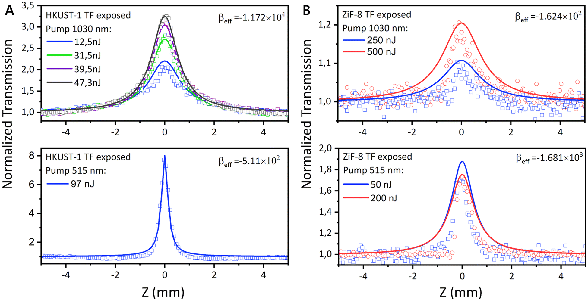 | ||
| Fig. 5 Open-aperture Z-scan curves for the pattern on HKUST-1 TF from Fig. 1B at 1030 nm and 515 nm wavelengths (A), and the pattern on ZIF-8 TF (B) at 1030 nm and 515 nm wavelengths with varying laser pulse energies (12.5 to 500 nJ). | ||
Additionally, after Z-scan experiments, we noticed no damage of the patterned TF. Therefore, the observed nonlinear optical effect, in combination with high laser damage stability of the patterns (up to TW cm−2), outlines their potential application for large-scale and nanometer-thick semi-transparent patterns for passive modulation devices and photonics in general.56–58
Conclusions
We report a one-step process to pattern MOF thin films through flashlight processing. Using a flash xenon lamp and a given mask, we developed arbitrary images on different MOF TFs in real time with cm2 s−1 speed and 70 μm spatial resolution. Structural and morphological analyses confirmed that the resulting patterns consist of carbon and metal derivatives. We also demonstrated that the resulting patterns act as visible and near-infrared light absorbers: Z-scan revealed that the patterns demonstrated the saturation absorption process with a nonlinear absorption coefficient up to 104 cm GW−1, which exceeds that of most metal films, initial MOFs, and metal–carbon hybrids. Thus, these results, open up a universal one-step approach to optically pattern MOFs (Table 1) for nonlinear optics in the desired ways.Experimental section
HKUST-1 thin film synthesis
Thin films were synthesized on the self-made spin coating setup (see Video S1, ESI†) with two microfluidic pumps and a two-dimensional positioner system. The Menzel glass, used as a wafer, has been previously sonified in isopropanol. Two microfluidic pumps were filled with Cu(NO3)2 and BTC (1,3,5-benzenetricarboxylate) solutions in ethanol (1.5 mmol and 3 mmol per 100 mL of ethanol, respectively). A rotating sample holder (300 rpm) has been previously heated up to 100 °C. Drops were released from pumps one by one – two drops per each of 700 cycles, while drop counting was controlled by an optical pair feedback system. Each cycle takes approximately 10 s, which means that the deposition of one film takes two hours, without any control required from the setup operator. By the end of the synthesis procedure, films were dried in air on the sample holder heated up to 70 °C for 15 min.Powder X-ray diffraction
The PXRD analysis of the film was performed using a Rigaku SmartLab 3 X-ray diffractometer (Tokyo, Japan) with a 2 kW characteristic CuKα (Kα1λ = 1.54059 Å, angular range 2θ = 5°−45°) X-ray radiation source and the Bragg–Brentano goniometer geometry. The measurements were performed with an angular resolution of 0.01° at a scanning speed of 0.7° min−1. The analysis confirmed the HKUST-1 structure (Fig. S1, ESI†) based on the merging of diffraction peaks with the etalon samples from the Cambridge Crystallographic Data Centre (CCDC numb. 112954).Microscopic imaging
Microscopic images of HKUST-1 thin films were acquired using a Karl Zeiss AxioImager A2m in a bright-field regime.Scanning electron microscopy and elemental analysis
SEM micrographs were obtained using a Carl Zeiss Neon 40 EsB CrossBeam system, being a combination of a field emission electron-optical column GEMINI and a field emission ion column with a gallium source, focused on a single point of the sample. The Neon 40 system uses three types of signal detectors: a secondary electron detector (In-lens SE) built into the column to study the surface topography with high resolution; a detector of reflected electrons with the possibility of energy filtering (EsB); and an Evernhart-Thornley secondary electron detector (SE). For obtaining the images of the patterns, the system was operated in a high-resolution field emission SEM mode, in combination with elemental analysis. The sample was mounted on a translation stage inside the chamber (stage positioning: X/Y = 152 mm, Z = 43 mm, tilt −15° − +65°, rotation 360°).Flashlight processing
For flashlight processing of MOF thin films, we designed the setup based on a pulsed Xe lamp (emission spectrum in Fig. S17, ESI†). The condenser battery charged for the estimate value ignited the discharge of the Xe lamp, thus creating the high-temperature plasma channel, irradiating the sample with the high-intensity full-spectrum pulsed light. In order to achieve the optimal distribution of the irradiance field, the reflector was used. The MOF thin film was placed at a distance of 2 cm from the light source, while the amount of energy put in the discharge (0.51 ± 0.04 J cm−2 and more, see Table S2, ESI†) was regulated via the initial voltage (1.00 ± 0.05 kV) on the condenser battery. The time needed for cm2 flashlight patterning varied from 1 s to 2 min, depending on the number of pulses (for more technical details, see the detailed description of the setup in the ESI† and Video S2).Confocal transmission and reflection spectroscopy
Confocal transmission and reflection measurements were performed on a self-made confocal optical setup. A halogen lamp (Avantes Hal-s mini) was used as the light source. For transmission measurements, the incoming light was focused via the bottom objective (Mitutoyo M Plan Apo x50, NA = 0.55) and transmitted light was collected with the top one (Mitutoyo M Plan Apo x50, NA = 0.55). For the reflection, the top objective was used both for focusing the incoming radiation on the TF, and for collecting the reflected light. In both cases, the collected signal was transferred to a Horiba Labram spectrometer with 150 g mm−1 diffraction grating and a water-cooling ANDOR CCD detector.Confocal Raman spectroscopy
Raman scattering measurements were implemented under excitation by a 632.8 nm He-Ne continuous laser radiation in the reflection mode through 100×/0.9 NA objective. To prevent the TF from unintended overheating, the integral power of He-Ne was limited with a natural density filter by 10% (from 25 mW to 2.5 mW). The collected signal was transferred to a Horiba Labram Spectrometer with 1800 g mm−1 diffraction gratings and a water-cooling ANDOR CCD detector.Z-scan measurements
The optical setup for Z-scan analysis is based on the fs pulsed ANTAUS fiber laser (Avesta projects) with the main harmonic wavelength of 1030 nm and a pulse duration of 270 fs. The main laser is also occupied with the second and third harmonic generators, which provides the conversion of the main wavelength into 515 nm. The pulse repetition rate was adjusted using the laser operational software, while the energy per pulse was regulated with the polarization attenuator (Glan-Taylor prism with rotating half wavelength plate). A telescope system was mounted with two long-working distance objectives, 10×/0.26NA Mitutoyo Plan Apo NIR. The pulse energy measurements of the incoming and the transmitted pulses were conducted using two Ophir Photonics PD10C detectors. The vertical translation of the sample (along the Z axis) was provided using a Standa Motorized Stage 8MT177-100.Author contributions
V. A. M. and N. A. Z. conceptualized the work. L. V., R. C., and M. M. performed the flashlight processing. Y. K. performed optical spectroscopy. S. A. P. performed z-scan experiments. S. S. R. and A. V. L. performed MOF thin film synthesis. S. A. S. performed bimetallic HKUST-1 synthesis. M. V. T. performed structural analysis. All the authors participated in writing the text.Data availability
The data supporting this article have been included as part of the ESI.†Conflicts of interest
There are no conflicts to declare.Acknowledgements
V. A. M. acknowledges the CPJ project (ANR-22-CPJ1–0010–01) of the French Agence Nationale de la Recherche. The authors acknowledge A. Efimova and P. Alekseevskiy (ITMO University) for assistance in confocal Raman analysis.Notes and references
- H. C. Zhou, J. R. Long and O. M. Yaghi, Introduction to Metal–Organic Frameworks, Chem. Rev., 2012, 112, 673–674 CrossRef CAS PubMed.
- Z. Ji, H. Wang, S. Canossa, S. Wuttke and O. M. Yaghi, Pore Chemistry of Metal–Organic Frameworks, Adv. Funct. Mater., 2020, 30, 2000238 CrossRef CAS.
- M. Kadhom and B. Deng, Metal-Organic Frameworks (MOFs) in Water Filtration Membranes for Desalination and Other Applications, Appl. Mater. Today, 2018, 11, 219–230 CrossRef.
- C. Jiang, L. Wang, Y. Ouyang, K. Lu, W. Jiang, H. Xu, X. Wei, Z. Wang, F. Dai and D. Sun, Recent Advances in Metal–Organic Frameworks for Gas Adsorption/Separation, Nanoscale Adv., 2022, 4, 2077–2089 RSC.
- D. Yang and B. C. Gates, Catalysis by Metal Organic Frameworks: Perspective and Suggestions for Future Research, ACS Catal., 2019, 9, 1779–1798 CrossRef CAS.
- H. Wang, Q. L. Zhu, R. Zou and Q. Xu, Metal–Organic Frameworks for Energy Applications, Chem, 2017, 2, 52–80 CAS.
- O. M. Yaghi, M. O’Keeffe, N. W. Ockwig, H. K. Chae, M. Eddaoudi and J. Kim, Reticular Synthesis and the Design of New Materials, Nature, 2003, 423, 705–714 CrossRef CAS PubMed.
- Y. Katayama, M. Kalaj, K. S. Barcus and S. M. Cohen, Self-Assembly of Metal–Organic Framework (MOF) Nanoparticle Monolayers and Free-Standing Multilayers, J. Am. Chem. Soc., 2019, 141, 20000–20003 CrossRef CAS PubMed.
- C. Avci, I. Imaz, A. Carné-Sánchez, J. A. Pariente, N. Tasios, J. Pérez-Carvajal, M. I. Alonso, A. Blanco, M. Dijkstra, C. López and D. Maspoch, Self-Assembly of Polyhedral Metal–Organic Framework Particles into Three-Dimensional Ordered Superstructures, Nat. Chem., 2017, 10, 78–84 CrossRef PubMed.
- A. Carné-Sánchez, I. Imaz, M. Cano-Sarabia, D. Maspoch and A. Spray-Drying, Strategy for Synthesis of Nanoscale Metal–Organic Frameworks and Their Assembly into Hollow Superstructures, Nat. Chem., 2013, 5, 203–211 Search PubMed.
- Q. Xiong, Y. Chen, D. Yang, K. Wang, Y. Wang, J. Yang, L. Li and J. Li, Constructing Strategies for Hierarchically Porous MOFs with Different Pore Sizes and Applications in Adsorption and Catalysis, Mater. Chem. Front., 2022, 6, 2944–2967 Search PubMed.
- C. Crivello, S. Sevim, O. Graniel, C. Franco, S. Pané, J. Puigmartí-Luis and D. Muñoz-Rojas, Advanced Technologies for the Fabrication of MOF Thin Films, Mater. Horizons, 2021, 8, 168–178 RSC.
- V. Stavila, A. A. Talin and M. D. Allendorf, MOF-Based Electronic and Opto-Electronic Devices, Chem. Soc. Rev., 2014, 43, 5994–6010 RSC.
- N. Kulachenkov, Q. Haar, S. Shipilovskikh, A. Yankin, J. F. Pierson, A. Nominé and V. A. Milichko, MOF-Based Sustainable Memory Devices, Adv. Funct. Mater., 2021, 32, 2107949 CrossRef.
- Z.-Z. Ma, Q.-H. Li, Z. Wang, Z.-G. Gu and J. Zhang, Electrically regulating nonlinear optical limiting of metal-organic framework film, Nat. Commun., 2022, 13, 6347 CrossRef CAS PubMed.
- N. Kulachenkov, M. Barsukova, P. Alekseevskiy, A. A. Sapianik, M. Sergeev, A. Yankin, A. A. Krasilin, S. Bachinin, S. Shipilovskikh, P. Poturaev, N. Medvedeva, E. Denislamova, P. S. Zelenovskiy, V. V. Shilovskikh, Y. Kenzhebayeva, A. Efimova, A. S. Novikov, A. Lunev, V. P. Fedin and V. A. Milichko, Dimensionality Mediated Highly Repeatable and Fast Transformation of Coordination Polymer Single Crystals for All-Optical Data Processing, Nano Lett., 2022, 22(17), 6972–6981 CrossRef CAS PubMed.
- Y. Liang, W. Hu, X. Yuan, Z. Zeng, B. Zhu and Y. Gu, Switchable Nonlinear Optical Absorption of Metal–Organic Frameworks, Adv. Opt. Mater., 2022, 10, 2200779 CrossRef CAS.
- Z.-B. Jin, G. Zhou, Y. Han, Z. Huang, Z.-G. Gu and J. Zhang, Topochemical Polymerization at Diacetylene Metal–Organic Framework Thin Films for Tuning Nonlinear Optics, J. Am. Chem. Soc., 2024, 146, 25016–25027 CrossRef CAS PubMed.
- C. Li, G. Qian and Y. Cui, Metal–organic frameworks for nonlinear optics and lasing, Info. Funct. Mater., 2024, 1, 125–159 Search PubMed.
- N. K. Kulachenkov, S. Bruyere, S. A. Sapchenko, Y. A. Mezenov, D. Sun, A. A. Krasilin, A. Nominé, J. Ghanbaja, T. Belmonte, V. P. Fedin, E. A. Pidko and V. A. Milichko, Ultrafast Melting of Metal–Organic Frameworks for Advanced Nanophotonics, Adv. Funct. Mater., 2019, 30, 1908292 CrossRef.
- E. V. Gunina, N. A. Zhestkij, M. Sergeev, S. V. Bachinin, Y. A. Mezenov, N. K. Kulachenkov, M. Timofeeva, V. Ivashchenko, A. S. Timin, S. A. Shipilovskikh, A. A. Yakubova, D. I. Pavlov, A. S. Potapov, J. Gong, L. Khamkhash, T. S. Atabaev, S. Bruyere and V. A. Milichko, Laser-Assisted Design of MOF-Derivative Platforms from Nano- to Centimeter Scales for Photonic and Catalytic Applications, ACS Appl. Mater. Interfaces, 2023, 15, 47541–47551 CrossRef CAS PubMed.
- R. Ma, H. Jiang, C. Wang, C. Zhao and H. Deng, Multivariate MOFs for Laser Writing of Alloy Nanoparticle Patterns, Chem. Comm., 2020, 56, 2715–2718 RSC.
- H. Jiang, S. Jin, C. Wang, R. Ma, Y. Song, M. Y. Gao, X. Liu, A. Shen, G. J. Cheng and H. Deng, Nanoscale Laser Metallurgy and Patterning in Air Using MOFs, J. Am. Chem. Soc., 2019, 141, 5481–5489 CrossRef CAS PubMed.
- R. Bo, M. Taheri, H. Chen, J. Bradford, N. Motta, S. Surve, T. Tran-Phu, P. Garg, T. Tsuzuki, P. Falcaro and A. Tricoli, Paper-Like Writable Nanoparticle Network Sheets for Mask-Less MOF Patterning, Adv. Funct. Mater., 2022, 32, 2100351 CrossRef CAS.
- M. Tu, B. Xia, D. E. Kravchenko, M. L. Tietze, A. J. Cruz, I. Stassen, T. Hauffman, J. Teyssandier, S. De Feyter, Z. Wang, R. A. Fischer, B. Marmiroli, H. Amenitsch, A. Torvisco, M. de, J. Velásquez-Hernández, P. Falcaro and R. Ameloot, Direct X-Ray and Electron-Beam Lithography of Halogenated Zeolitic Imidazolate Frameworks, Nat. Mater., 2020, 20, 93–99 CrossRef PubMed.
- X. Tian, F. Li, Z. Tang, S. Wang, K. Weng, D. Liu, S. Lu, W. Liu, Z. Fu, W. Li, H. Qiu, M. Tu, H. Zhang and J. Li, Crosslinking-induced patterning of MOFs by direct photo- and electron-beam lithography, Nat. Commun., 2024, 15, 2920 CrossRef CAS PubMed.
- M. de, J. Velásquez-Hernández, M. Linares-Moreau, L. A. Brandner, B. Marmiroli, M. Barella, G. P. Acuna, S. Dal Zilio, M. F. K. Verstreken, D. E. Kravchenko, O. M. Linder-Patton, J. D. Evans, H. Wiltsche, F. Carraro, H. Wolinski, R. Ameloot, C. Doonan and P. Falcaro, Fabrication of 3D Oriented MOF Micropatterns with Anisotropic Fluorescent Properties, Adv. Mater., 2023, 25, 2211478 Search PubMed.
- H. Liu, W. Lin and M. Hong, Surface coloring by laser irradiation of solid substrates, APL Photon, 2019, 4, 051101 CrossRef CAS.
- J. Geng, L. Xu, W. Yan, L. Shi and M. Qiu, High-speed laser writing of structural colors for full-color inkless printing, Nat. Commun., 2023, 14, 565 CrossRef CAS PubMed.
- X. Zhu, W. Yan, U. Levy, N. A. Mortensen and A. Kristensen, Resonant laser printing of structural colors onhigh-index dielectric metasurfaces, Sci. Adv., 2017, 3, e1602487 CrossRef PubMed.
- T. H. Im, J. H. Lee, H. S. Wang, S. H. Sung, Y. B. Kim, Y. Rho, J. H. Park and K. J. Lee, Flashlight-Material Interaction for Wearable and Flexible Electronics, Mater. Today, 2021, 51, 525–551 CrossRef CAS.
- S. S. A. Chui, S. M.-F. Lo, J. P. H. Charmant, A. G. Orpen and I. D. Williams, A Chemically Functionalizable Nanoporous Material [Cu3(TMA)2(H2O)3]N, Science, 1999, 283, 1148–1150 CrossRef CAS PubMed.
- L. Chen, H.-F. Wang, C. Li and Q. Xu, Bimetallic metal–organic frameworks and their derivatives, Chem. Sci., 2020, 11, 5369–5403 RSC.
- M. J. Van Vleet, T. Weng, X. Li and J. R. Schmidt, In Situ, Time-Resolved, and Mechanistic Studies of Metal–Organic Framework Nucleation and Growth, Chem. Rev., 2018, 118, 3681–3721 CrossRef CAS PubMed.
- L. Huelsenbeck, S. Jung, R. Herrera, P. V. Balachandran and G. Giri, Accelerated HKUST-1 Thin-Film Property Optimization Using Active Learning, ACS Appl. Mater. Interfaces, 2021, 13, 61827–61837 CrossRef CAS PubMed.
- Y. Wang, Y. Lü, W. Zhan, Z. Xie, Q. Kuang and L. Zheng, Synthesis of Porous Cu2O/CuO Cages Using Cu-Based Metal–Organic Frameworks as Templates and Their Gas-Sensing Properties, J. Mater. Chem. A, 2015, 3, 12796–12803 RSC.
- Y. A. Mezenov, S. Bruyere, A. Krasilin, E. Khrapova, S. V. Bachinin, P. V. Alekseevskiy, S. Shipiloskikh, P. Boulet, S. Hupont, A. Nomine, B. Vigolo, A. S. Novikov, T. Belmonte and V. A. Milichko, Insights into Solid-To-Solid Transformation of MOF Amorphous Phases, Inorg. Chem., 2022, 61, 13992–14003 CrossRef CAS PubMed.
- P. V. Alekseevskiy, M. Timofeeva, S. Bachinin, R. Peignier, C. Noel, P. Boulet, T. Belmonte and V. A. Milichko, Non-thermal plasma etching of MOF thin films in high optical quality for interference sensing, Opt. Mater., 2024, 154, 115666 Search PubMed.
- M. Born and E. Wolf, Principles of Optics, Pergamon Press, United Kindom, 1959 Search PubMed.
- Y. A. Mezenov, S. Bruyere, N. K. Kulachenkov, A. N. Yankin, S. S. Rzhevskiy, P. V. Alekseevskiy, V. D. Gilemkhanova, S. V. Bachinin, V. Dyachuk, A. A. Krasilin, J. Zollinger, T. Belmonte, A. Nominé and V. A. Milichko, Probing the Dynamics of Cu Nanoparticle Growth inside Metal–Organic Frameworks upon Electron Beam Irradiation, Photon. Nanostruct. Fund. App., 2020, 41, 100832 CrossRef.
- Z. Li, L. Deng, I. A. Kinloch and R. J. Young, Raman spectroscopy of carbon materials and their composites: Graphene, nanotubes and fibres, Prog. Mater. Sci., 2023, 135, 101089 CrossRef CAS.
- S. Guo, Y. Zhao, H. Yuan, C. Wang, H. Jiang and G. J. Cheng, Ultrafast Laser Manufacture of Stable, Efficient Ultrafine Noble Metal Catalysts Mediated with MOF Derived High Density Defective Metal Oxides, Small, 2020, 16, 2000749 CrossRef CAS PubMed.
- X. Liu, L. An, S. Xiang, H. Jiang and G. J. Cheng, 3D MOF Nanoarchitecture Membrane via Ultrafast Laser Nanoforging, Small Meth, 2021, 5, 2100758 CrossRef CAS PubMed.
- A. Basu, K. Roy, N. Sharma, S. Nandi, R. Vaidhyanathan, S. Rane, C. Rode and S. Ogale, CO2 Laser Direct Written MOF-Based Metal-Decorated and Heteroatom-Doped Porous Graphene for Flexible All-Solid-State Microsupercapacitor with Extremely High Cycling Stability, ACS Appl. Mater. Interfaces, 2016, 8, 31841–31848 CrossRef CAS PubMed.
- Y. Tang, H. Zheng, Y. Wang, W. Zhang and K. Zhou, Laser-Induced Annealing of Metal–Organic Frameworks on Conductive Substrates for Electrochemical Water Splitting, Adv. Funct. Mater., 2021, 31, 2102648 CrossRef CAS.
- J. Zou, H. Dong, H. Wu, J. Huang, X. Zeng, Y. Dou, Y. Yao and Z. Li, Laser-induced rapid construction of Co/N-doped honeycomb-like carbon networks as oxygen electrocatalyst used in zinc-air batteries, Carbon, 2022, 200, 462–471 CrossRef CAS.
- N. Zhestkij, A. Efimova, S. Rzhevskiy, Y. Kenzhebayeva, S. Bachinin, E. Gunina, M. Sergeev, V. Dyachuk and V. A. Milichko, Reversible and Irreversible Laser Interference Patterning of MOF Thin Films, Crystals, 2022, 12, 846 CrossRef CAS.
- N. A. Zhestkij, A. S. Efimova, Y. Kenzhebayeva, S. A. Povarov, P. V. Alekseevskiy, S. S. Rzhevskiy, S. A. Shipilovskikh and V. A. Milichko, Grayscale to Multicolor Laser Writing Inside a Label-Free Metal-Organic Frameworks, Adv. Funct. Mater., 2024, 34, 2311235 CrossRef CAS.
- R. Ameloot, M. B. J. Roeffaers, G. De Cremer, F. Vermoortele, J. Hofkens, B. F. Sels and D. E. De Vos, Metal–Organic Framework Single Crystals as Photoactive Matrices for the Generation of Metallic Microstructures, Adv. Mater., 2011, 23, 1788–1791 CrossRef CAS PubMed.
- G. Lu, O. K. Farha, W. Zhang, F. Huo and J. T. Hupp, Engineering ZIF-8 Thin Films for Hybrid MOF-Based Devices, Adv. Mater., 2012, 24, 3970–3974 CrossRef CAS PubMed.
- M. Sheik-bahae and A. A. Said, E. W. Van Stryland, High-Sensitivity, Single-Beam N_2 Measurements, Opt. Lett., 1989, 14, 955 CrossRef CAS PubMed.
- A. Volpi, J. Kock, A. R. Albrecht, M. P. Hehlen, R. I. Epstein and M. Sheik-Bahae, Open-aperture Z-scan study for absorption saturation: accurate measurement of saturation intensity in YLF:Yb for optical refrigeration, Opt. Lett., 2021, 46, 1421–1424 CrossRef PubMed.
- D. J. Li, Q. Li, Z. G. Gu and J. Zhang, Oriented Assembly of 2D Metal-Pyridylporphyrinic Framework Films for Giant Nonlinear Optical Limiting, Nano Lett., 2021, 21, 10012–10018 CrossRef CAS PubMed.
- Y. Liang, W. Qiao, T. Feng, B. Zhang, Y. Zhao, Y. Song, T. Li and C. Kränkel, Investigation on the Optical Nonlinearity of the Layered Magnesium-Mediated Metal Organic Framework (Mg-MOF-74), Opt. Express, 2021, 29, 23786 CrossRef CAS PubMed.
- Z. Z. Ma, Q. H. Li, Z. Wang, Z. G. Gu and J. Zhang, Electrically Regulating Nonlinear Optical Limiting of Metal-Organic Framework Film, Nat. Comm., 2022, 13, 6347 CrossRef CAS PubMed.
- I. L. Gomes de Souza and V. F. Rodriguez-Esquerre, Design of planar and wideangle resonant color absorbers for applications in the visible spectrum, Sci. Rep., 2019, 9, 7045 CrossRef PubMed.
- Y. Takashima, S. Furuta, K. Nagamatsu, M. Haraguchi and Y. Naoi, Broadband Ag/SiO2/Fe/TiO2 ultrathin planar absorber with a wide acceptance angle from visible to near-infrared regions, Opt. Mater. Express, 2024, 14, 778–791 CrossRef CAS.
- C.-S. Park and S.-S. Lee, Narrowband and flexible perfect absorber based on a thin-film nano-resonator incorporating a dielectric overlay, Sci. Rep., 2020, 10, 17727 CrossRef CAS PubMed.
Footnote |
| † Electronic supplementary information (ESI) available. See DOI: https://doi.org/10.1039/d5qm00166h |
| This journal is © the Partner Organisations 2025 |