
 Open Access Article
 This Open Access Article is licensed under a Creative Commons Attribution-Non Commercial 3.0 Unported Licence
Effect of annealing temperature on the properties of CsPbBr3 nanocrystal films via inkjet printing and its application in colour conversion layers†
Junaid
Khan
 *a,
Júlia
Marí-Guaita
a,
Kenneth
Lobo
a,
Giovanni
Vescio
a,
Carina
Pareja-Rivera
b,
Iván
Mora-Seró
b,
Sergi
Hernández
a,
Albert
Cirera
a and
Blas
Garrido
a
*a,
Júlia
Marí-Guaita
a,
Kenneth
Lobo
a,
Giovanni
Vescio
a,
Carina
Pareja-Rivera
b,
Iván
Mora-Seró
b,
Sergi
Hernández
a,
Albert
Cirera
a and
Blas
Garrido
a
aMIND-IN2UB, Department of Electronics and Biomedical Engineering, University of Barcelona, Carrer Martí i Franquès 1, 08028, Barcelona, Spain. E-mail: junaidkhan@ub.edu
bInstitute of Advanced Materials (INAM), Universitat Jaume I, Castelló de la Plana, Spain
First published on 21st July 2025
Abstract
Inkjet printing has emerged as a sustainable and scalable approach for fabricating electronic and optoelectronic devices, offering precise material deposition with minimal waste. Among solution-processable materials, metal halide perovskites, particularly CsPbBr3, have gained significant attention due to their exceptional optoelectronic properties, including high photoluminescence quantum yield, tuneable bandgap, and efficient charge transport. However, optimizing the inkjet-printing process remains a challenge, particularly post printing annealing since CsPbBr3 nanocrystals are sensitive to environmental conditions. In this study, we systematically investigate the effect of annealing temperature on the structural, morphological, and photoluminescence properties of inkjet-printed CsPbBr3 films. Our results reveal that thermal treatment plays a pivotal role in controlling grain size, crystallinity, defect density, and overall optoelectronic behaviour. Notably, a remarkable 70-fold enhancement in photoluminescence emission was observed, alongside a crystal structure morphology evolution from 3D to 0D and 2D structures through simple annealing offering transformative potential for optoelectronic applications. By elucidating the interplay between annealing conditions and film characteristics, this work provides key insights for optimizing inkjet-printed perovskite films, driving advancements in next-generation, sustainable, and high-performance printed electronics. The application of the printed films was successfully demonstrated as efficient colour conversion layers for optoelectronic devices.
1. Introduction
Printed electronics are emerging as a sustainable alternative to traditional lithographic processes for developing eco-friendly electronic devices.1–3 There are various methods for fabricating printed electronics, such as inkjet printing, screen printing, gravure printing, flexographic printing, offset printing, and direct digital ink writing.4–6 Among these, inkjet printing stands out for its numerous advantages, including its non-contact nature and scalability, while minimizing material waste and reducing energy consumption.7,8 Moreover, inkjet printing supports eco-friendly, water-based inks, eliminates the need for hazardous chemicals, and enables low-temperature processing, making it compatible with biodegradable substrates. Additionally, the technology allows for on-demand customization, scalable production, and the integration of diverse functional materials such as dielectric, conductive, and semiconducting inks.7,9 By reducing environmental impact and enabling the creation of flexible, recyclable, and energy-efficient designs, inkjet printing aligns closely with the goals of sustainable electronics manufacturing.10–12 The research and development of solution processability of many functional inks have further widened their applications in various fields. These include inks based on carbon materials such as graphene and carbon nanotubes, gold (Au) nanoparticles, silver (Ag) nanoparticles, halide-based and non-halide based perovskites, and biomolecules.8Besides various advantages, inkjet printing has challenges related to film uniformity, reproducibility of results, and interfacial adhesion compared to conventional lithographic and spin-coating techniques. These limitations arise due to inconsistent droplet formation, variations in ink spreading, and weak adhesion to substrates. To overcome these issues, it is crucial to optimize key parameters such as ink formulation (viscosity, surface tension, and solvent composition), substrate properties (surface energy and wettability), and annealing conditions (temperature, duration, and atmosphere). Fine-tuning these factors ensures uniform jetting, improved ink-substrate interaction, enhanced film morphology, and superior device performance, making inkjet printing a viable alternative for high-precision applications.
For optoelectronics applications, halide perovskites are emerging as leading candidates due to their outstanding properties, such as a tuneable bandgap, high absorption coefficients, long carrier diffusion lengths, and low trap-state densities, making them highly suitable for applications in solar cells, LEDs, photodetectors, and lasers.13–15 Halide perovskites also possess excellent charge-carrier mobility, low exciton binding energy, and high photoluminescence quantum yields, enabling efficient light emission and energy conversion. Additionally, they are solution-processable, enabling low-cost fabrication of thin films using scalable techniques like inkjet printing.16 Their versatility in composition and structure allows for tailoring material properties to specific device requirements, solidifying their potential in next-generation optoelectronics.
Besides these remarkable properties, halide perovskites also present certain limitations. Notably, the susceptibility of CsPbX3 (X = Cl, Br, I) to environmental factors like moisture, heat, and UV light poses significant challenges for commercialization. However, these limitations can be addressed by encapsulation methods.17 The combination of solution processing for CsPbBr3 with inkjet printing enables the development of devices with a broad range of applications.
The performance of inkjet-printed devices is strongly influenced by various factors, including ink rheology, substrate interactions, and the post-printing annealing process, as previously discussed. Many previous studies have outlined the importance of annealing conditions in the final properties of their inks. For instance, Secor et al.,18 studied the impact of intense pulsed light (IPL) annealing of graphene inks on various substrates such as polyester, poly(ethylene naphthalate), glass and polyimide. They concluded that IPL annealing effectively reduces the sheet resistance of graphene films on various substrates (PET, PEN, PI, and glass), with required pulse energy varying based on each substrate's thermal properties. Another study by Woo et al.,19 reported annealing temperature significantly affects the resistivity of printed silver films. As the temperature increases, resistivity generally decreases due to improved particle sintering and interparticle connectivity. This effect is most notable in films from stable dispersions, which show the lowest resistivity at higher temperatures, particularly at 400 °C, where uniform microstructures with minimal pores are achieved.
CsPbBr3 nanocrystals, being highly sensitive to thermal treatment and environmental conditions due to their ionic crystal structure and weak ligand bonding, undergo significant structural and morphological changes upon annealing, directly impacting the optoelectronic properties of the fabricated devices.20–22 Grain size and film morphology are critical factors that govern charge transport, defect density, and overall device efficiency, all of which are highly sensitive to annealing conditions. However, despite its pivotal role in scalable manufacturing, the impact of annealing temperature on inkjet-printed CsPbBr3 films remains largely unexplored. A comprehensive investigation into this aspect is essential to unlock new pathways for optimizing device performance while ensuring a sustainable and efficient fabrication process.
In this study, we conduct a comprehensive investigation into the effect of annealing temperature on the chemical composition, structural evolution, surface morphology, and photoluminescence characteristics of inkjet-printed CsPbBr3 films. Our findings reveal critical thermally induced transformations directly influencing film quality and optoelectronic performance. By optimizing the annealing process, we achieve enhanced crystallinity, morphological changes, improved charge transport, and a remarkable increase in photoluminescence emission. Furthermore, we demonstrate the practical application of these printed films as high-performance colour conversion layers, highlighting their potential for next-generation optoelectronic and display technologies. These insights pave the way for advancing inkjet-printed perovskite materials in sustainable and scalable device fabrication.
2. Experimental
2.1. Materials
All the compounds, materials, and solvents used to synthesize the CsPbBr3 nanocrystals were employed as received from their corresponding provider companies without any further purification. Lead(II) bromide (PbBr2, ABCR, 99.999%), cesium carbonate (Cs2CO3, Sigma-Aldrich, 99.995%), 1-octadecene (1-ODE, Sigma-Aldrich, 90%), oleic acid (OA, Sigma-Aldrich, 90%), oleylamine (OLA, Sigma-Aldrich, 90%), hexane (Hx, Sigma-Aldrich, 99%), dodecane (Sigma-Aldrich, anhydrous ≥99%) methyl acetate (MeOAc, Sigma-Aldrich, 99.5%).![[thin space (1/6-em)]](https://www.rsc.org/images/entities/char_2009.gif) :1 OA/oleylamine (OLA) solution (10 mL) under nitrogen. The temperature was raised to 170 °C, and 4 mL Cs-oleate was injected. After 5 seconds, the reaction was quenched in an ice bath. For the purification of nanocrystals, the crude reaction mixture was centrifuged (5000 rpm, 5 min), the supernatant was discarded, and the precipitate was redispersed in hexane (Hx, 5 ml). The MeOAc (5 ml) was added to the dispersion, followed by a second centrifugation (5000 rpm, 5 min). The supernatant was discarded, and the solid was redispersed in Hx (2 ml). The dispersion was stored at −18 °C overnight, then carefully decanted and filtered to remove the solid sediment deposited at the bottom. In all cases, the dispersion was transferred to a glass vial, dried under a gentle nitrogen flow, and placed under vacuum for 15 minutes to obtain CsPbBr3 nanoparticles as a solid. Finally, the solid was weighed and redispersed in the appropriate volume of Hx or dodecane to achieve the desired concentration and filtered through a 0.42 μm Teflon filter. The schematic of the synthesis process is given in Fig. 1(a).
:1 OA/oleylamine (OLA) solution (10 mL) under nitrogen. The temperature was raised to 170 °C, and 4 mL Cs-oleate was injected. After 5 seconds, the reaction was quenched in an ice bath. For the purification of nanocrystals, the crude reaction mixture was centrifuged (5000 rpm, 5 min), the supernatant was discarded, and the precipitate was redispersed in hexane (Hx, 5 ml). The MeOAc (5 ml) was added to the dispersion, followed by a second centrifugation (5000 rpm, 5 min). The supernatant was discarded, and the solid was redispersed in Hx (2 ml). The dispersion was stored at −18 °C overnight, then carefully decanted and filtered to remove the solid sediment deposited at the bottom. In all cases, the dispersion was transferred to a glass vial, dried under a gentle nitrogen flow, and placed under vacuum for 15 minutes to obtain CsPbBr3 nanoparticles as a solid. Finally, the solid was weighed and redispersed in the appropriate volume of Hx or dodecane to achieve the desired concentration and filtered through a 0.42 μm Teflon filter. The schematic of the synthesis process is given in Fig. 1(a).
 | ||
| Fig. 1 (a) Schematic illustration of the CsPbBr3 nanocrystal synthesis process. (b) Ink formulation and printing steps: (b1) Ink preparation and deposition, (b2) measurement of the contact angle, (b3) digital photograph of the printed film under illumination, (b4) SEM image showing the surface morphology, and (b5) annealing process for film formation. | ||
:1 volume ratio (dodecane:hexane). The NC concentration was adjusted to 10 wt% and were vigorously stirred using a vortex mixer for 3 minutes at room temperature. The resulting perovskite NC ink was then ready for inkjet printing to obtain nanofilms. The obtained colloidal solution was also characterized for absorption, PL and morphology as shown in Fig. S1(a and b).†
Dimatix piezoelectric drop-on-demand (DOD) inkjet printer (DMP2831 Fujifilm Dimatix Inc.) was used for printing with a drop spacing of 20 μm. SiO2/Si substrates was used as substrate which was cleaned using acetone and isopropanol solvents and were dried using a nitrogen gun. The substrate was chosen for its excellent wettability with our ink and thermal stability, making it suitable for studying the effects of high-temperature annealing. A Samba cartridge with 12 nozzles, each delivering a native drop volume of 2.4 pL, was employed to ensure precise deposition. The viscosity and surface tension of the NC ink were carefully optimized to achieve smooth, uniform and consistent printability, following the protocols established in our prior studies.16
The printed films were fabricated by printing two layers of the NC ink to ensure pinhole-free uniform and continuous wet film. After printing, the samples were subjected to annealing at varied temperatures of 45 °C, 90 °C, 120 °C, 150 °C, 180 °C, and 200 °C for 20 minutes under vacuum conditions (60 mbar) in an oven. Each sample was labelled according to its respective annealing temperature and stored in a vacuum desiccator to preserve their structural and compositional integrity for further characterization.
2.2. Characterization
Scanning electron microscopy (SEM) images were obtained using the FEGSEM – JEOL 3100F system. TEM analysis was conducted using a JEM-2010F TEM/STEM (JEOL Ltd, Japan) operated at an acceleration voltage of 200 kV. High-resolution TEM images were obtained using JEM-ARM200F: NEOARM TEM microscope. For spherical morphologies, diameters were measured across 100 nanocrystals, while cubic structures were analysed from the TEM images by determining their edge lengths, ensuring accurate morphological quantification.Morphology of the samples were also observed via atomic force microscopy (AFM) using a Digital Instruments Nanoscope D-5000, scanning the x–y plane with a z-axis resolution of approximately 1 nm. The crystalline microstructure, orientation, and nanocrystal (NC) were characterized through X-ray diffraction (XRD) using a Japan Rigaku D/Max-IIA diffractometer with Cu Kα radiation (λ = 1.5406 Å) operating at 40 keV and 40 mA.
The chemical composition and local environment of the printed perovskite NC layers were examined via X-ray photoelectron spectroscopy (XPS) using a PHI ESCA-5500 spectrometer with monochromatic Al Kα radiation (E = 1486 eV) at 350.0 W. The X-ray source and detector positioned at 45.1° angle relative to the sample normal.
The photoluminescence (PL) properties of the films deposited on SiO2/Si substrates were investigated by exciting the samples with a 325 nm He–Cd laser at a power density of 50 mW, in a spot size of about 80 μm in diameter. The emitted light was analysed using a single-grating monochromator coupled to a GaAs photomultiplier. To ensure the reliability of the photoluminescence intensity comparisons across samples, PL spectra were acquired at three distinct points on each film. The measured values showed minimal variation (below 15%), indicating a high degree of uniformity. In addition, new samples were fabricated and measured under identical conditions to confirm reproducibility. The photostability of the samples was further assessed by monitoring the PL intensity over 150 seconds under continuous laser illumination. The emission remained stable throughout, with fluctuations below 5%, confirming that the excitation conditions did not induce photodegradation during the measurements. These results are presented in ESI Fig. S4.† The observed PL intensity trends remained consistent across all measurements, validating the robustness of the annealing-dependent behaviour.
The absorption spectra of the colloidal solution were acquired using the JASCO V-780 UV-Visible/NIR Spectrophotometer, which features a double-beam, single monochromator with dual gratings for UV-Visible and NIR, and a PMT detector for UV-Visible. The absolute photoluminescence quantum yield (PLQY) of the perovskites colloidal solution was estimated using the Absolute QY Measurement System C9920-02, equipped with an integrating sphere and excited with a wavelength of 405 nm.
3. Results and discussion
The printing process and annealing of the CsPbBr3 films on Si/SiO2 substrates are illustrated in Fig. 1(b1). The surface tension, viscosity, and density of the CsPbBr3 ink were measured to be 27 dynes per cm, 2.5 cP, and 1.08 g cm−3, respectively. Based on these rheological parameters (Tables S1 and S2†), the calculated Z value for the ink is Z = 12. This value falls within the optimal range of 1 < Z < 14 indicating the potential for stable droplet formation during the inkjet printing process.24The average contact angle was measured as shown in Fig. 1(b2) using a contact angle goniometer, which was found to be approximately 24°, indicating good wettability with the SiO2/Si substrate. These parameters are extremely important to maintain the printing properties and performance of the fabricated device.1,2 As shown in Fig. 1(b3), the CsPbBr3 forms a continuous film, demonstrating uniform coverage. Upon illumination, the film exhibits fluorescent green emission typically observed for CsPbBr3 printed films. The SEM image demonstrates uniform coverage of the nanocrystals across the film (Fig. 1(b4)). The annealing conditions to develop uniform films is illustrated in Fig. 1(b5).
3.1. Crystalline structure and phase evolution
The crystalline structure of the perovskite films annealed at varying temperatures provides critical insights into their structural and phase properties. X-ray diffraction (XRD) analysis was performed for all annealed samples to examine the crystal quality, phase composition, and the presence of any secondary phases or impurities. The diffraction peaks’ peak positions, intensities, and full width at half-maximum (FWHM) provide valuable information about lattice constants, crystallite size, and strain within the films. Furthermore, peak shifts or broadening variations can indicate structural integrity changes or thermal-induced modifications.The XRD patterns of the inkjet-printed CsPbBr3 thin films annealed at various temperatures are presented in Fig. 2(a), enabling a comprehensive comparison of the structural evolution with the annealing temperature. The XRD pattern showed two prominent diffraction peaks at 2θ = 15.18° and 30.64°, corresponding to the {100} and {200} crystallographic planes, respectively. These peaks were significantly more intense compared to other peaks typically observed in cubic phase CsPbBr3 nano-cubes (Pm![[3 with combining macron]](https://www.rsc.org/images/entities/char_0033_0304.gif) m), as shown from the JCPDS 00-054-0752 Cubic CsPbBr3. These include peaks at 21.55° ({110}), 26.48° ({111}), 37.56° ({210}), and 43.62° ({211}).
m), as shown from the JCPDS 00-054-0752 Cubic CsPbBr3. These include peaks at 21.55° ({110}), 26.48° ({111}), 37.56° ({210}), and 43.62° ({211}).
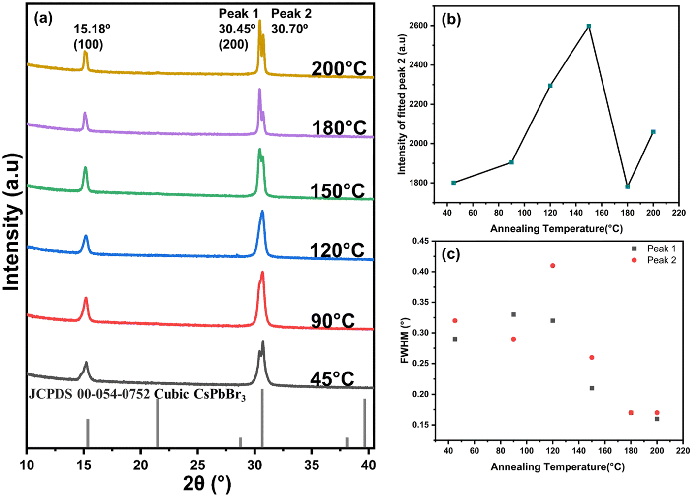 | ||
| Fig. 2 (a) X-ray diffraction patterns of CsPbBr3 nanocrystals annealed at different temperatures, showing the evolution of crystallinity and phase stability. (b) The intensity variation of the fitted (200) peak with annealing temperature indicates the optimal temperature for enhanced crystallinity. (c) FWHM analysis of peaks 1 and 2, demonstrating the effect of annealing on crystallite size and structural order. | ||
The dominance of the (100) and (200) peaks indicate a preferential crystallographic orientation of the inkjet-printed CsPbBr3 films, likely induced by the controlled inkjet printing deposition process and subsequent annealing. This preferential orientation reflects the structural uniformity and alignment of the nano cubes within the printed films.14,25,26 The preferential orientations can be observed in the high resolution TEM image as shown in Fig. S1(c).†
The peaks observed at 2θ ≈ 30° in the sample annealed at 45 °C exhibited splitting, suggesting the presence of an intermediate phase attributed to solvent retention and initial crystal growth.27 At higher annealing temperatures (90 °C and 120 °C), this peak merged into a single broad peak, likely due to the overlap of two phases. Interestingly, at 150 °C, the overlapped peak split into two distinct peaks at 2θ = 30.45° and 30.70°, with the latter showing higher intensity and persisting up to this temperature, suggesting the presence of two separate phases in the inkjet-printed films.
For better comparison, the peaks were deconvoluted into two peaks as shown in Fig. S2.† The maximum intensity of the fitted peak 2 was plotted against annealing temperature, as shown in Fig. 2(b). An increase in secondary phase formation was observed with increasing temperature, suggesting that higher temperatures favour secondary phase formation. However, at 180 °C, a sudden drop in intensity was observed, indicating a transformation of the secondary phase back into the primary perovskite phase. Interestingly, at 200 °C, the secondary phase re-emerged.
This secondary phase formation is likely due to the structural transformation of cubic CsPbBr3 into tetragonal Cs4PbBr6 or CsPb2Br5 phases at high temperatures.26 The observed peak splitting could be attributed to the coexisting multiple crystalline phases or lattice distortions induced by thermal stress. Additionally, a slight shift in peak position was observed at 180 °C and 200 °C, which can be attributed to thermal expansion of the unit cell.28
The full-width at half-maximum of the primary diffraction peaks corresponding to the (200) planes became narrower progressively with increasing annealing temperature, signifying enhanced crystallinity, as plotted for both peaks found at 2θ ≈ 30°, as shown in Fig. 2(c). This improvement is associated with Ostwald ripening, resulting in larger grain sizes and reduced lattice strain,28 which is attributed to increased energy availability for larger grain formation and the elimination of residual solvents during annealing.
3.2. Morphological evolution and TEM analysis
To gain deeper insights into the structural modifications observed in the XRD analysis, transmission electron microscopy (TEM) was employed to investigate the corresponding morphological changes, providing a direct correlation between structural alterations and morphology at the nanoscale. The TEM images, presented in Fig. 3, provide critical insights into the nanoscale structural features of the CsPbBr3 films annealed at different temperatures. CsPbBr3 perovskites are known to crystallize in orthorhombic, tetragonal, and cubic polymorphs within the perovskite lattice, with the cubic phase representing the high-temperature state for all compositions.29 | ||
| Fig. 3 TEM analysis of CsPbBr3 nanocrystals annealed at different temperatures. (a1–f1) TEM images showing the overall morphology of nanocrystals annealed at (a) 45 °C, (b) 90 °C, (c) 120 °C, (d) 150 °C, (e) 180 °C, and (f) 200 °C. (a2–f2) Magnified TEM images highlighting the detailed morphology of nanocrystals. (a3–f3) Size distribution histograms corresponding to the respective annealing temperatures, based on the measurements of 100 nanocrystals using ImageJ software. | ||
At lower annealing temperatures of printed films (45 °C and 90 °C), the TEM images reveal well-defined cubic morphologies with average edge lengths of 10.3 ± 2.4 nm and 18.5 ± 4.7 nm, respectively, as calculated for nanocrystals using ImageJ software (Table 1). These nano cubes exhibit a uniform size distribution, with a small fraction of globular structures with unclear edges observed at 90 °C, as highlighted in yellow in Fig. 3b. The cubic phase, confirmed by XRD analysis, indicates stability under low thermal stress, with the preferential crystallographic orientation of the cubes further corroborating the results obtained in the XRD analysis.
| Annealing temperature (°C) | Morphology | Average size (nm) | SD (nm) | Min size (nm) | Max size (nm) |
|---|---|---|---|---|---|
| 45 | 3D cubes | 10.3 | 2.4 | 5.6 | 15.8 |
| 90 | 3D cubes and 0 D | 18.5 | 4.7 | 8.9 | 34.0 |
| 120 | 0 D | 25.7 | 6.7 | 12.9 | 44.0 |
| 150 | 0 D | 25.4 | 7.5 | 7.4 | 47.4 |
| 180 | 2D nanoplatelets | 23.0 | 9.1 | 11.3 | 60.8 |
| 200 | 0 D | 110.3 | 74.3 | 26.0 | 325.2 |
As the annealing temperature increased to 120 °C and 150 °C, a pronounced morphological transformation occurred. TEM images indicate the replacement of cubic structures by globular morphologies with unclear edges, with average diameters of 25.7 ± 6.7 nm and 25.4 ± 7.5 nm, respectively, in both cases compatible with a bimodal distribution. The globular morphology can be related to the disassociation of 3D CsPbBr3 into 0D Cs4PbBr6.30 The transformation of 3D CsPbBr3 to 0D Cs4PbBr6via thermal annealing occurs through a structural reorganization driven by the increased temperature. The mechanism behind this transition involves Pb–Br network degradation, forming isolated [PbBr6]4− octahedrons stabilized by additional Cs+ ions.
This transition is accompanied by peak splitting observed in the XRD, indicating phase coexistence and lattice distortions. Besides, the initial transformation at 120 °C would induce lower crystalline quality, as confirmed by maximum FWHM in Fig. 2c. This transformation is driven by size expansion, as evidenced by the larger globular morphology of 0D Cs4PbBr6 compared to the cubic structures of CsPbBr3, with the dark spots on 0D Cs4PbBr6 indicating the presence of heavier Pb atoms.31–34 This observation is consistent with the findings of Tian et al.,35 in which they demonstrated the conversion of 3D CsPbBr3 to 0D Cs4PbBr6. They found that inorganic cations (e.g., Cs+) and ligands (e.g., didodecyldimethylammonium bromide, DDAB), used in the synthesis of CsPbBr3 nanocrystals (NC) at ambient temperature, rapidly induced this transformation. A similar morphological transformation from 3D to 0D was reported by Rao et al.,36 in which the globular-shaped 0D Cs4PbBr6 were observed by adjusting the Oleyl Amine (OA) concentration. This transformation is attributed to crystal anisotropy driven by growth kinetics, where capping ligands preferentially bind to specific crystal facets, leading to facet-dependent growth rates and ultimately altering the perovskite morphology. However, our study reports the transformation by just thermal annealing. The observed changes highlight the significant role of thermal energy in driving the rearrangement of nanocrystal surfaces and altering their morphology.
At 180 °C, a remarkable transformation was observed, as a square-like morphology of nanoplatelets with well-defined edges was observed as evident from the TEM images (Fig. 3(e)). The average crystal size was determined to be 23.05 ± 9.10 nm, exhibiting a broader size distribution compared to lower temperature samples. Notably, the prevalence of globular morphologies decreased significantly, giving rise to distinct nanoplatelet-like structures, as illustrated in Fig. 3(e1 and e2). This transformation is further supported by the XRD, where the intensity of peaks associated with secondary phases diminishes substantially, indicating the conversion into 2D nanosheet-like structures. This suggests that 180 °C represents a critical annealing temperature at which sufficient thermal energy enables surface atom diffusion and recrystallization, that might have resulted in conversion of irregular or globular shapes 0D Cs4PbBr6 into a more stable, layered CsPbBr3 nanoplatelets-like structure.37 The nanoplatelet-like structure was further confirmed using AFM microscopy, as shown in Fig. S3.† The AFM images of the sample annealed at 180 °C reveal numerous stacked nanosheet-like structures of varying sizes, ranging from 20 to 200 nm, consistent with observations from TEM images. To obtain a more precise measurement of thickness, a smaller scan area of 0.5 μm was measured for larger nanosheets, as depicted in Fig. 4(a). The measured thickness and corresponding line profile are presented in Fig. 4(b). The line profile indicates the presence of multiple stacked nanosheets with a thickness of 30 nm and a lateral size of 200 nm, further supporting the conclusion that annealing at 180 °C promotes the transformation from cubes to nanosheet-like structures. The transformation from 3D structures to 0D nanocrystals and subsequently into 2D nanosheet-like formations is distinctly illustrated in Fig. 4(c).
 | ||
| Fig. 4 Atomic force microscopy (AFM) analysis of the nanosheet-like structures formed after annealing at 180 °C (a) High-resolution AFM image of a selected region, highlighting a large nanosheet with a line scan for thickness measurement. (b) Corresponding height profile extracted from the line scan, indicating a nanosheet thickness of approximately 30 nm. (c) Schematic illustration of the morphological changes from 3D to 0D to 2D. | ||
This morphological evolution observed in the TEM images suggests a growth mechanism driven by Ostwald ripening. This hypothesis aligns with prior studies of in situ TEM investigations, where the growth of nanocrystals (NC) was monitored on a heated TEM grid, as reported by Hoffman et al.38 Ostwald ripening is a process wherein smaller, less stable particles gets sacrificed and contribute to the growth of larger, energetically more stable particles. This phenomenon results in a reduction in the total number of particles, as evidenced by the diminished number of nanocrystals observed in the TEM images (Fig. 3(f)). Further investigation is required to determine the exact reason for the change in the morphology and atomic composition from 3D CsPbBr3 nano cubes to 0D Cs4PbBr6 at 120 °C and 150 °C and recrystallization to 2D CsPbBr3 nanoplatelets at 180 °C.
At 200 °C, a significant deviation from the nanoplatelets like morphology is observed. Fig. 3(f) show irregularly shaped nanocrystals, with an average size of 110.3 ± 74.3 nm. The large standard deviation reflects extensive size variation and irregularity due to the nanocrystals’ coalescence, sintering, and partial decomposition. These observations align with the XRD analysis formation of secondary phase. The elevated thermal energy at 200 °C compromises the structural integrity of the nanocrystals, leading to morphological degradation and irregular growth.
The average size and morphology of CsPbBr3 nanocrystals also exhibit distinct trends with annealing temperature as shown in Table 1. At lower temperatures, the stability of the cubic phase is associated with relatively small and uniform nanocrystals.14 With increasing temperature, the transition to globular morphologies occurs alongside a growth in size, peaking at 200 °C with significant irregularity. The largest nanoplatelets are observed at 180 °C, indicating this as the optimal annealing condition for achieving the desired nanoplatelets like morphology with larger crystalline size.
3.3. XPS analysis and chemical state modifications
To further investigate the functional groups and chemical states present on the surface of the samples, XPS analysis was conducted. The survey spectra for all samples are presented in Fig. 5(a). The survey XPS spectra given in Fig. 5(a) for CsPbBr3 nanocrystals annealed at various temperatures reveal the presence of characteristic peaks corresponding to Cs 3d, Pb 4f, Br 3d, O 1s, C 1s, and N 1s. The dominant peaks associated with Cs, Pb, and Br confirm the elemental composition of CsPbBr3, whereas the peaks for C 1s and O 1s may originate from adventitious carbon from the remaining solvent and capping agents. The adsorbed oxygen present on the sample surface is likely due to environmental exposure, a common observation in XPS analysis of perovskites and other nanomaterials.39,40 Additionally, the presence of N 1s could indicate the remnants capping ligands used during synthesis, which play a crucial role in stabilizing the nanocrystals.41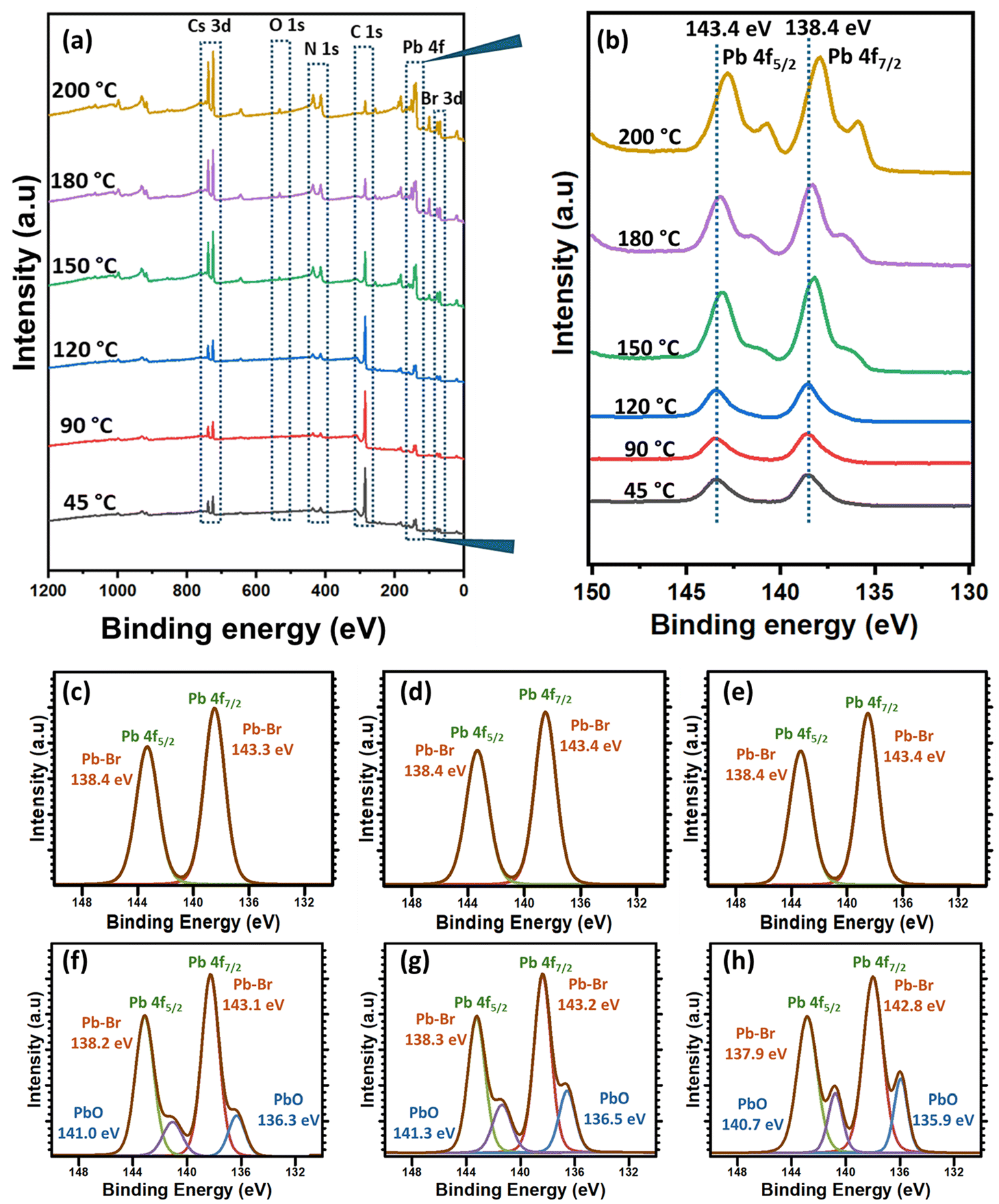 | ||
| Fig. 5 X-ray photoelectron spectroscopy (XPS) analysis of CsPbBr3 films annealed at different temperatures. (a) Survey spectra showing elemental composition across various annealing temperatures. (b) High-resolution XPS spectra of the Pb 4f region, highlighting Pb 4f5/2 and Pb 4f7/2 peaks. (c–h) Deconvoluted Pb 4f spectra at different temperatures (c) 45 °C, (d) 90 °C, (e)120 °C, (f)150 °C (g) 180 °C (h) 200 °C, indicating contributions from Pb–Br bonding and PbO formation. The shifting of peaks suggests changes in chemical states due to thermal annealing. | ||
The survey spectrum exhibits notable changes with annealing temperature. At lower annealing temperatures (45 °C, 90 °C and 120 °C), the C 1s peaks are sharper and more prominent. However, these peaks diminish drastically at higher temperatures (150, 180, and 200 °C), with the minimum at 200 °C. This is likely due to solvent evaporation as well as decomposition of capping ligands. Furthermore, the intensity of Cs 3d, Br 3d, O1s and Pb 3f peaks increases for samples annealed at 150, 180 and 200 °C, suggesting the formation of secondary species, a phenomenon also observed in the XRD and TEM images.
The systematic shift in the Pb 4f binding energy also correlates with changes in the Br 3d region, where a slight shift to lower binding energies is observed with increasing temperature. This suggests that changes in the local bonding environment of Pb are mirrored by corresponding changes in the Br chemical state, further confirming the thermal-induced structural modifications of the CsPbBr3 lattice as shown in Fig. 5(b).
The high-resolution spectra of the Pb 4f region provide more detailed insights into the chemical state of lead within the samples. The Pb 4f peaks consist of two primary components: Pb 4f7/2 and Pb 4f5/2, resulting from spin–orbit coupling.42 At lower annealing temperatures, the Pb 4f7/2 peak appears at ∼138.4 eV, characteristic of Pb–Br bonds in the CsPbBr3 lattice. However, as the annealing temperature increases, a systematic shift in the Pb 4f peaks to lower binding energies is observed, with the Pb 4f7/2 peak shifting to ∼137.9 eV at 200 °C. This shift reflects changes in the chemical environment surrounding Pb atoms, potentially due to lattice restructuring, a reduction in surface defects, or partial oxidation of lead.
Deconvolution of the Pb 4f peaks provides further insights into the chemical states of Pb as shown in Fig. 5(c–h). Two distinct components are resolved: Pb–Br, corresponding to lead in the CsPbBr3 perovskite lattice, and Pb–O, indicative of oxidized lead species on the sample surface. At lower temperatures, the Pb–Br component dominates, confirming the integrity of the perovskite structure. However, with increasing annealing temperature, the relative intensity of the Pb–O component becomes more pronounced, especially at 200 °C, indicating an increase in surface oxidation. This is consistent with the concurrent increase in the O 1s peak in the survey spectra, which suggests the formation of lead oxide species. The enhanced oxidation at higher temperatures can be attributed to thermal degradation or exposure to ambient conditions during the annealing process.
3.4. Photoluminescence analysis and optical properties
The observed structural, morphological, and chemical modifications discussed earlier directly influence the photoluminescence spectra of the samples. Accordingly, PL measurements were performed, and the relative intensities with different annealing temperatures are depicted in Fig. 6(a). | ||
| Fig. 6 (a) Photoluminescence (PL) analysis of inkjet-printed CsPbBr3 films annealed at different temperatures. PL spectra showing a significant enhancement in emission intensity with increasing annealing temperature, with the highest intensity observed at 180 °C. The inset depicts the normalized PL spectra, highlighting the shift in peak position. (b) Maximum PL intensity as a function of annealing temperature, demonstrating a remarkable 70-fold increase at 180 °C before decreasing at 200 °C, indicating the critical role of thermal treatment in optimizing optoelectronic properties. (inset) Without CsPbBr3 nanocrystals (blue emission) Colour conversion using CsPbBr3 nanocrystals (green emission). | ||
At the lowest annealing temperature (45 °C), a single fluorescence peak cantered around 520 nm is observed, corresponding to the PL emission of nanocrystalline CsPbBr3. The PL intensity at this stage appears relatively low, possibly due to the smaller crystal size and the presence of surface defects or residual solvents, which may contribute to non-radiative recombination.
At 90 °C, the PL intensity increases noticeably. This enhancement can be attributed to the growth of nanocrystals, as evidenced by TEM images showing larger cube sizes. The improved crystallinity and reduced surface defects at this stage result in more efficient radiative recombination, contributing to the higher PL intensity.
At 120 °C, a significant drop in PL intensity is observed. This decrease can be related to morphological changes, where nanocrystals transition into non- 0D globular shaped Cs2PbBr6, as well as phase separation, as indicated by XPS and TEM analysis and is characteristics feature on non-luminescent 0D Cs4PbBr6. Although the 0D Cs4PbBr6 crystals are reported to be non-luminescent, the emission reported in this study could be due to the presence of embedded CsPbBr3 nanocrystalline phase inside the 0D Cs4PbBr6 crystals.43
Interestingly, at 150 °C, the PL intensity increases again, which might indicate further growth of nanocrystalline embedded CsPbBr3 inside the 0D Cs4PbBr6 matrix. The evidence of growth is also observed from the low-resolution TEM images given in Fig. 3, where the darker image contrast represents embedded CsPbBr3 as compared to 0D Cs4PbBr6 crystals. The darker contrast is due to the presence of higher density of heavier Pb atoms, whereas a lighter contrast indicates the presence of lighter atoms.
Similar structure is reported by Sun et al.,30 in which the origin of green emission in 0D Cs4PbBr6 crystals was observed due to the presence of embedded nanocrystalline CsPbBr3 grown due to the lack of Cs+ atoms which was controlled by varying the Cs:Pb ratio. The mechanism of Cs4PbBr6 formation is closely related to the dissociation and rearrangement of [PbBr6]4− octahedrons due to thermal stress, coupled with an excess of Cs+ ions. Under thermal activation, the [PbBr6]4− octahedrons partially dissociate, weakening their direct connections and facilitating the interaction with excess Cs+ ions. This results in the formation of a polymerized framework where [PbBr6]4− units are linked through Cs+ ions, forming a –PbBr6–Cs-PbBr6–Cs– structure. This polymerized linkage subsequently rearranges into the 0D Cs4PbBr6 perovskite phase, where the [PbBr6]4− octahedra are isolated from each other by Cs+ ions, leading to its characteristic zero-dimensional crystal structure. However, in certain conditions, particularly when there is an excess of [PbBr6]4− octahedrons beyond what is required to stabilize the 0D Cs4PbBr6 phase, some of these octahedrons can remain intact and crystallize into CsPbBr3 nanocrystals within the Cs4PbBr6 matrix. The embedded CsPbBr3 nanocrystals (NC) are a result of local phase segregation, where regions of higher Pb2+ and Br− concentration facilitate the formation of the 3D CsPbBr3 perovskite phase inside the Cs4PbBr6 domains. This leads to the coexistence of both the zero-dimensional 0D Cs4PbBr6 and 2D CsPbBr3 within the same material, creating a raisin bread like structure with unique optical and electronic properties.
At 180 °C, a remarkable increase in PL intensity of nearly 70 times higher than that of the sample annealed at 45 °C is observed, representing the highest fluorescence among all samples. This pronounced enhancement is attributed to the complete crystallization of CsPbBr3 nanocrystals into well-defined 2D nanosheets, as confirmed by TEM analysis (Fig. 3 and Table 1). The formation of 2D structures introduces quantum confinement effects along the thickness direction, especially when the nanosheet thickness approaches or falls below the Bohr exciton radius of CsPbBr3 (∼7 nm). While the lateral size of the sheets remains large, confinement in the vertical (z) axis can still significantly influence the excitonic properties, leading to enhancement in photoluminescence. In addition to confinement, thermal annealing promotes improved crystallinity and surface passivation, reducing trap states that typically facilitate non-radiative recombination. This combination of dimensional confinement, enhanced structural order, and fewer surface defects contributes to the substantial increase in radiative recombination efficiency, thereby intensifying the PL emission.44
At 200 °C, the PL intensity decreases significantly, indicating degradation of the crystal structure and the formation of a multiphase material. The XPS analysis corroborates this observation, suggesting the emergence of additional non-radiative recombination pathways due to the breakdown of the perovskite lattice and the presence of defect states.
In addition to the changes in intensity, the PL peak position exhibits distinct shifts with annealing temperature, reflecting the variations in nanocrystal size and phase composition. This trend is clearly illustrated in the normalized PL spectra shown in inset of Fig. 6(a), where the peak intensity was normalized for a better comparison of the shifts.
At lower annealing temperatures (45 °C to 90 °C), the emission remains centred around 519 nm, corresponding to smaller CsPbBr3 nanocrystals. As the annealing temperature increases to 120 °C and 150 °C, the PL spectrum broadens slightly, indicating a mixture of nanocrystalline and bulk-like phases. At 180 °C, the PL peak shifts slightly toward longer wavelengths (∼523 nm), indicating a redshift associated with the transition to crystals with larger lateral sizes. At 200 °C, the emission is at ∼521 nm, but the intensity diminishes significantly due to the degradation of the perovskite structure and the formation of multiphase materials.
3.5. Interplay between morphology, crystal size, and optical properties
The observed shifts in peak position and changes in PL intensity highlight the interplay between morphology, crystal size and optical properties in inkjet-printed films. The redshift for sample annealed at 180 °C corresponds to the emergence of larger crystal structure of CsPbBr3 as compared to the smaller CsPbBr3 nano crystallites inside the 0D Cs4PbBr6 which is also evidence from the TEM images in which perfectly larger square shaped nanosheets are observed.30These findings emphasize the need of optimizing annealing conditions to precisely control phase stability, crystallite size, and defect density that affect both the structural and optical properties of CsPbBr3 films for optoelectronic applications. While moderate annealing (90 °C–150 °C) facilitates improved crystallinity and passivation, excessive annealing at 200 °C leads to structural degradation and defect formation. Further experimental data of in situ characterization are required to further confirm the mechanism of morphological changes. Characterization techniques such as in situ real-time XRD, PL lifetime measurements, and grazing-incidence wide-angle X-ray scattering (GIWAXS) would be beneficial. These techniques would provide direct insights into crystal phase transitions, charge carrier dynamics, and structural evolution during annealing.
The inset image in Fig. 6(b) demonstrates the application of the inkjet-printed sample as a colour conversion layer, where the blue emission transitions into green. The inset image in Fig. 6(b) demonstrates the effective colour conversion mechanism of the inkjet-printed CsPbBr3 film, where incident blue light is transformed into green emission. This process is governed by photoluminescent down-conversion, in which high-energy blue photons (typically ∼450–470 nm) emitted from a blue LED source are absorbed by the CsPbBr3 perovskite layer due to its suitable bandgap (∼2.3 eV). Upon absorption, electrons in the perovskite are excited from the valence band to the conduction band, forming excitons (electron–hole pairs). These excitons subsequently undergo radiative recombination, releasing photons in the green spectral range (∼520–540 nm). This emitted green light constitutes the observed color change, resulting from the intrinsic photoluminescence of CsPbBr3. The narrow emission bandwidth and high photoluminescence quantum yield (PLQY) of the perovskite ensure a saturated and efficient green output. The energy difference between the absorbed blue light and the emitted green light, known as the Stokes shift, also minimizes reabsorption losses, enhancing optical performance. Thus, the inkjet-printed CsPbBr3 layer functions as an efficient and stable color-conversion medium, converting blue excitation into a visually distinct green emission.
4. Conclusion
This study presents a comprehensive analysis of the impact of annealing temperature on the structural, morphological, and optoelectronic properties of inkjet-printed CsPbBr3 films. Our results reveal that thermal treatment plays a crucial role in modulating grain size, crystallinity, defect density, and photoluminescence characteristics, directly influencing device performance. Optimizing annealing conditions is essential for achieving high-quality perovskite films with enhanced charge transport and stability. Notably, annealing-induced structural transformations were observed, with 3D nano-cubes evolving into 0D structures at higher temperatures, while a nanoplatelet-like morphology emerged at 180 °C. Remarkably, a 70-fold enhancement in photoluminescence was achieved, underscoring the significance of these modifications for optoelectronic applications. Finally, the practical application of inkjet-printed CsPbBr3 films was demonstrated as efficient colour conversion layers, highlighting their potential for next-generation display and lighting technologies.Data availability
The data supporting this article have been included as part of the manuscript, in the “Methods” section, and in the ESI.† The datasets generated during and/or analysed during the current study are available from the corresponding author on reasonable request.Conflicts of interest
The authors declare that they have no known competing financial interests or personal relationships that could have appeared to influence the work reported in this paper.Acknowledgements
This work was funded by the Ministry of Science and Innovation of Spain under the projects LIP-FREE (PID2022-140978OB-I00) and PIXIE-SENS (PDC2023-145804-I00). This work has been partially supported by PROMETEO Program from Generalitat Valenciana (Q-Solutions project reference CIPROM/2021/078). J. Marí-Guaita acknowledges the financial backing from grant JDC2022-049260-I funded by the Spanish Ministry of Science and Innovation and by the European Union Next Generation EU/PRTR.References
- J. Khan and M. Mariatti, Effect of natural surfactant on the performance of reduced graphene oxide conductive ink, J. Cleaner Prod, 2022, 376, 134254, DOI:10.1016/j.jclepro.2022.134254.
- J. Khan, M. Mariatti, S. A. Zubir, A. Rusli, A. A. Manaf and R. K. Khirotdin, Eco-friendly alkali lignin-assisted water-based graphene oxide ink and its application as a resistive temperature sensor, Nanotechnology, 2024, 35, 055301, DOI:10.1088/1361-6528/ad06d4.
- J. Khan, V. Rezo, T. Vincze, M. Weis, S. A. Momin, N. El-Atab and M. Jaafar, Flexible and highly selective NO2 gas sensor based on direct-ink-writing of eco-friendly graphene oxide for smart wearable application, Chemosphere, 2024, 367, 143618, DOI:10.1016/j.chemosphere.2024.143618.
- Y. Bonnassieux, C. J. Brabec, Y. Cao, T. B. Carmichael, M. L. Chabinyc, K.-T. T. Cheng, G. Cho, A. Chung, C. L. Cobb, A. Distler, H.-J. J. Egelhaaf, G. Grau, X. Guo, G. Haghiashtiani, T.-C. C. Huang, M. M. Hussain, B. Iniguez, T.-M. M. Lee, L. Li, Y. Ma, D. Ma, M. C. McAlpine, T. N. Ng, R. Österbacka, S. N. Patel, J. Peng, H. Peng, J. Rivnay, L. Shao, D. Steingart, R. A. Street, V. Subramanian, L. Torsi and Y. Wu, The 2021 flexible and printed electronics roadmap, Flexible Printed Electron., 2021, 6, 023001, DOI:10.1088/2058-8585/abf986.
- J. Lemarchand, N. Bridonneau, N. Battaglini, F. Carn, G. Mattana, B. Piro, S. Zrig and V. Noël, Challenges, Prospects, and Emerging Applications of Inkjet-Printed Electronics: A Chemist's Point of View, Angew. Chem., Int. Ed., 2022, 61, e202200166, DOI:10.1002/ANIE.202200166.
- K. Zhu, G. Vescio, S. González-Torres, J. López-Vidrier, J. L. Frieiro, S. Pazos, X. Jing, X. Gao, S. D. Wang, J. Ascorbe-Muruzábal, J. A. Ruiz-Fuentes, A. Cirera, B. Garrido and M. Lanza, Inkjet-printed h-BN memristors for hardware security, Nanoscale, 2023, 15, 9985–9992, 10.1039/D3NR00030C.
- J. Khan, M. Weis and M. Mariatti, Inkjet-Printed Temperature Sensor From Eco-Friendly Edge-Oxidized Graphene Oxide Ink on Biodegradable Polyvinyl Alcohol Substrate, IEEE Sens. Lett., 2024, 8, 1–4, DOI:10.1109/LSENS.2024.3414427.
- S. F. Kamarudin, N. H. Abdul Aziz, H. W. Lee, M. Jaafar and S. Sulaiman, Inkjet Printing Optimization: Toward Realization of High-Resolution Printed Electronics, Adv. Mater. Technol., 2024, 9, 2301875, DOI:10.1002/ADMT.202301875.
- M. A. Fakhri, J. Khan, M. Mariatti, Z. Ain Abdul Hamid, K. I. K. Marsilla, V. Vilay and M. Todo, The influence of working distance, stirring and electrospinning time on fibre forming properties of electrospun polylactic acid for facemask layer application, Mater. Today: Proc., 2022, 66, 2742–2746, DOI:10.1016/j.matpr.2022.06.507.
- J. Khan and M. Mariatti, In situ graphene oxide reduction via inkjet printing using natural reducing inks, Flexible Printed Electron., 2023, 8, 035009, DOI:10.1088/2058-8585/acf143.
- R. Islam, S. Afroj, J. Yin, K. S. Novoselov, J. Chen, N. Karim, M. R. Islam, S. Afroj, N. Karim, J. Yin, J. Chen and K. S. Novoselov, Advances in Printed Electronic Textiles, Adv. Sci., 2024, 11, 2304140, DOI:10.1002/ADVS.202304140.
- G. Vescio, D. N. Dirin, S. González-Torres, J. Sanchez-Diaz, R. Vidal, I. P. Franco, S. Das Adhikari, V. S. Chirvony, J. P. Martínez-Pastor, F. A. Vinocour Pacheco, L. Przypis, S. Öz, S. Hernández, A. Cirera, I. Mora-Seró, M. V. Kovalenko and B. Garrido, Inkjet-Printed Red-Emitting Flexible LEDs Based on Sustainable Inks of Layered Tin Iodide Perovskite, Adv. Sustainable Syst., 2024, 8, 2400060, DOI:10.1002/ADSU.202400060.
- H. Jin, Y. J. Zeng, J. A. Steele, M. B. J. Roeffaers, J. Hofkens and E. Debroye, Phase stabilization of cesium lead iodide perovskites for use in efficient optoelectronic devices, NPG Asia Mater., 2024, 161(16), 1–18, DOI:10.1038/s41427-024-00540-0.
- G. Vescio, J. L. Frieiro, A. F. Gualdrón-Reyes, S. Hernández, I. Mora-Seró, B. Garrido and A. Cirera, High Quality Inkjet Printed-Emissive Nanocrystalline Perovskite CsPbBr3 Layers for Color Conversion Layer and LEDs Applications, Adv. Mater. Technol., 2022, 7, 2101525, DOI:10.1002/ADMT.202101525.
- H. P. Adl, J. Sánchez-Díaz, G. Vescio, A. Cirera, B. Garrido, F. A. V. Pacheco, W. Żuraw, Ł Przypis, S. Öz, I. Mora-Seró, J. P. Martínez-Pastor and I. Suárez, Tailoring Single-Mode Random Lasing of Tin Halide Perovskites Integrated in a Vertical Cavity, Adv. Mater., 2024, 36, 2313252, DOI:10.1002/ADMA.202313252.
- G. Vescio, G. Mathiazhagan, S. González-Torres, J. Sanchez-Diaz, A. Villaueva-Antolí, R. S. Sánchez, A. F. Gualdrón-Reyes, M. Oszajca, F. Linardi, A. Hauser, F. A. Vinocour-Pacheco, W. Żuraw, S. Öz, S. Hernández, I. Mora-Seró, A. Cirera and B. Garrido, Fully Inkjet-Printed Green-Emitting PEDOT:PSS/NiO/Colloidal CsPbBr3/SnO2 Perovskite Light-Emitting Diode on Rigid and Flexible Substrates, Adv. Eng. Mater., 2023, 25, 2300927, DOI:10.1002/adem.202300927.
- L. Yang, T. Wang, Q. Min, B. Liu, Z. Liu, X. Fan, J. Qiu, X. Xu, J. Yu and X. Yu, High Water Resistance of Monoclinic CsPbBr 3 Nanocrystals Derived from Zero-Dimensional Cesium Lead Halide Perovskites, ACS Omega, 2019, 4, 6084–6091, DOI:10.1021/ACSOMEGA.9B00370/ASSET/IMAGES/LARGE/AO-2019-003707_0004.JPEG.
- E. B. Secor, B. Y. Ahn, T. Z. Gao, J. A. Lewis and M. C. Hersam, Rapid and Versatile Photonic Annealing of Graphene Inks for Flexible Printed Electronics, Adv. Mater., 2015, 27, 6683–6688, DOI:10.1002/ADMA.201502866;REQUESTEDJOURNAL:JOURNAL:15214095;WGROUP:STRING:PUBLICATION.
- K. Woo, D. Jang, Y. Kim and J. Moon, Relationship between printability and rheological behavior of ink-jet conductive inks, Ceram. Int., 2013, 39, 7015–7021, DOI:10.1016/j.ceramint.2013.02.039.
- K. Satake, K. Narazaki, H. Abe, K. Yanagihashi, M. Mizukami, Y. Suzuri, T. Chiba and J. Kido, Low-Temperature Annealing of Inkjet-Printed CsPbBr 3 Perovskite Nanocrystal Film for Light-Emitting Diodes, ACS Appl. Nano Mater., 2024, 7, 11313–11319, DOI:10.1021/acsanm.4c00867.
- H. Lee, J. W. Jeong, M. G. So, G. Y. Jung and C. L. Lee, Design of Chemically Stable Organic Perovskite Quantum Dots for Micropatterned Light-Emitting Diodes through Kinetic Control of a Cross-Linkable Ligand System, Adv. Mater., 2021, 33, 2007855, DOI:10.1002/ADMA.202007855.
- M. Liu, Q. Wan, H. Wang, F. Carulli, X. Sun, W. Zheng, L. Kong, Q. Zhang, C. Zhang, Q. Zhang, S. Brovelli and L. Li, Suppression of temperature quenching in perovskite nanocrystals for efficient and thermally stable light-emitting diodes, Nat. Photonics, 2021, 155(15), 379–385, DOI:10.1038/s41566-021-00766-2.
- L. Protesescu, S. Yakunin, M. I. Bodnarchuk, F. Krieg, R. Caputo, C. H. Hendon, R. X. Yang, A. Walsh and M. V. Kovalenko, Nanocrystals of Cesium Lead Halide Perovskites (CsPbX3, X = Cl, Br, and I): Novel Optoelectronic Materials Showing Bright Emission with Wide Color Gamut, Nano Lett., 2015, 15, 3692–3696, DOI:10.1021/nl5048779.
- Y. Z. N. Htwe, M. Mariatti and J. Khan, Review on solvent- and surfactant-assisted water-based conductive inks for printed flexible electronics applications, J. Mater. Sci.:Mater. Electron., 2024, 35, 1191, DOI:10.1007/s10854-024-12927-4.
- B. D. Chernomordik, A. E. Béland, N. D. Trejo, A. A. Gunawan, D. D. Deng, K. A. Mkhoyan and E. S. Aydil, Rapid facile synthesis of Cu2ZnSnS4 nanocrystals, J. Mater. Chem. A, 2014, 2, 10389–10395, 10.1039/C4TA01658K.
- F. Palazon, F. Di Stasio, S. Lauciello, R. Krahne, M. Prato and L. Manna, Evolution of CsPbBr3 nanocrystals upon post-synthesis annealing under an inert atmosphere, J. Mater. Chem. C, 2016, 4, 9179–9182, 10.1039/c6tc03342c.
- J. Y. Woo, Y. Kim, J. Bae, T. G. Kim, J. W. Kim, D. C. Lee and S. Jeong, Highly Stable Cesium Lead Halide Perovskite Nanocrystals through in Situ Lead Halide Inorganic Passivation, Chem. Mater., 2017, 29, 7088–7092, DOI:10.1021/acs.chemmater.7b02669.
- F. Palazon, S. Dogan, S. Marras, F. Locardi, I. Nelli, P. Rastogi, M. Ferretti, M. Prato, R. Krahne and L. Manna, From CsPbBr3 Nano-Inks to Sintered CsPbBr3-CsPb2Br5 Films via Thermal Annealing: Implications on Optoelectronic Properties, J. Phys. Chem. C, 2017, 121, 11956–11961, DOI:10.1021/acs.jpcc.7b03389.
- W. Zhang, S. Huang, Y. Zhang, H. Lv, D. Ge, Y. Gu and M. Jiang, Cesium lead bromide perovskite nanocrystals for the visual detection of chloride ions: A review, J. Solid State Chem., 2024, 329, 124418, DOI:10.1016/J.JSSC.2023.124418.
- W. Sun, Y. T. Hung, W. T. Huang, R. S. Liu and W. Zhou, Photoluminescent Nano-CsPbBr3 Embedded in Cs4PbBr6 Crystals: Formation Mechanism and Properties, Cryst. Growth Des., 2024, 24, 545–553, DOI:10.1021/acs.cgd.3c01226.
- Z. Dang, J. Shamsi, F. Palazon, M. Imran, Q. A. Akkerman, S. Park, G. Bertoni, M. Prato, R. Brescia and L. Manna, In Situ Transmission Electron Microscopy Study of Electron Beam-Induced Transformations in Colloidal Cesium Lead Halide Perovskite Nanocrystals, ACS Nano, 2017, 11, 2124–2132, DOI:10.1021/ACSNANO.6B08324/ASSET/IMAGES/LARGE/NN-2016-08324D_0007.JPEG.
- Y. Liu, Y. Liu, C. Yang, L. Mei, H. Ding, R. Mi and Y. Zhang, Influence of Lewis basicity on the S2− induced synthesis of 0D Cs4PbBr6 hexagonal nanocrystals and its implications for optoelectronics, Chem. Sci., 2025, 16(6), 2741–2750, 10.1039/D4SC06515H.
- K. Wang, Y. Yuan, S. Du, Q. Yao, J. Zhang, C. Shang, C. Li, H. Sun, W. Zhang, J. Ding and T. Zhou, Understanding of the Photoluminescence Mechanism Based on Zero-Dimensional Cs4PbBr6- mXm (X = Cl, I) Single Crystals, J. Phys. Chem. C, 2021, 125, 15223–15232 CrossRef CAS . (accessed February 2, 2025): https://pubs.acs.org/doi/abs/10.1021/acs.jpcc.1c04696.
- G. Tong, H. Li, Z. Zhu, Y. Zhang, L. Yu, J. Xu and Y. Jiang, Enhancing Hybrid Perovskite Detectability in the Deep Ultraviolet Region with Down-Conversion Dual-Phase (CsPbBr3-Cs4PbBr6) Films, J. Phys. Chem. Lett., 2018, 9, 1592–1599, DOI:10.1021/ACS.JPCLETT.8B00429/SUPPL_FILE/JZ8B00429_SI_001.PDF.
- H. Tian, Y. Liu and F. L. Jiang, Chemical Instability of CsPbBr3 Nanocrystals and the Reversible Transformation between CsPbBr3 and Cs4PbBr6 Nanocrystals as Driven by Synthetic Precursors, Chem. Mater., 2024, 36, 35, DOI:10.1021/ACS.CHEMMATER.4C02018/ASSET/IMAGES/LARGE/CM4C02018_0009.JPEG.
- L. Rao, X. Ding, X. Du, G. Liang, Y. Tang, K. Tang and J. Z. Zhang, Ultrasonication-assisted synthesis of CsPbBr3 and Cs4PbBr6 perovskite nanocrystals and their reversible transformation, Beilstein J. Nanotechnol., 2019, 1066(10), 666–676, DOI:10.3762/BJNANO.10.66.
- L. Yang, D. Li, C. Wang, W. Yao, H. Wang and K. Huang, Room-temperature synthesis of pure perovskite-related Cs4PbBr6 nanocrystals and their ligand-mediated evolution into highly luminescent CsPbBr3 nanosheets, J. Nanopart. Res., 2017, 19, 1–13, DOI:10.1007/S11051-017-3959-7/TABLES/2.
- J. B. Hoffman, G. Zaiats, I. Wappes and P. V. Kamat, CsPbBr3 Solar Cells: Controlled Film Growth through Layer-by-Layer Quantum Dot Deposition, Chem. Mater., 2017, 29, 9767–9774, DOI:10.1021/ACS.CHEMMATER.7B03751/ASSET/IMAGES/LARGE/CM-2017-03751R_0005.JPEG.
- M. Liu, G. Zhong, Y. Yin, J. Miao, K. Li, C. Wang, X. Xu, C. Shen, H. Meng, M. Liu, Y. Yin, J. Miao, K. Li, C. Wang, X. Xu, C. Shen, H. Meng and G. Zhong, Aluminum-Doped Cesium Lead Bromide Perovskite Nanocrystals with Stable Blue Photoluminescence Used for Display Backlight, Adv. Sci., 2017, 4, 1700335, DOI:10.1002/ADVS.201700335.
- S. M. H. Qaid, H. M. Ghaithan, B. A. Al-Asbahi and A. S. Aldwayyan, Achieving Optical Gain of the CsPbBr3Perovskite Quantum Dots and Influence of the Variable Stripe Length Method, ACS Omega, 2021, 6, 5297–5309, DOI:10.1021/ACSOMEGA.0C05414/ASSET/IMAGES/LARGE/AO0C05414_M003.JPEG.
- M. Wang, S. Wang, R. Chen, M. Zhu, Y. Liu, H. Ding, J. Ren, T. Xuan and H. Li, Highly Efficient and Stable CsPbBr3-Alginic Acid Composites for White Light-Emitting Diodes, Coatings, 2023, 13, 1062, DOI:10.3390/COATINGS13061062.
- I. S. Zhidkov, D. W. Boukhvalov, A. F. Akbulatov, L. A. Frolova, L. D. Finkelstein, A. I. Kukharenko, S. O. Cholakh, C. C. Chueh, P. A. Troshin and E. Z. Kurmaev, XPS spectra as a tool for studying photochemical and thermal degradation in APbX3 hybrid halide perovskites, Nano Energy, 2021, 79, 105421, DOI:10.1016/J.NANOEN.2020.105421.
- X. Yu, L. Wu, H. Hu, M. Chen, Y. Tan, D. Yang, Q. Pan, Q. Zhong, T. Supasai and Q. Zhang, Cs4PbX6 (X = Cl, Br, I) Nanocrystals: Preparation, Water-Triggered Transformation Behavior, and Anti-Counterfeiting Application, Langmuir, 2018, 34, 10363–10370, DOI:10.1021/acs.langmuir.8b01683.
- Z. Yang, M. Wang, H. Qiu, X. Yao, X. Lao, S. Xu, Z. Lin, L. Sun and J. Shao, Engineering the Exciton Dissociation in Quantum-Confined 2D CsPbBr3 Nanosheet Films, Adv. Funct. Mater., 2018, 28, 1–10, DOI:10.1002/adfm.201705908.
Footnote |
| † Electronic supplementary information (ESI) available. See DOI: https://doi.org/10.1039/d5nr01385b |
| This journal is © The Royal Society of Chemistry 2025 |