
 Open Access Article
 This Open Access Article is licensed under a
 Creative Commons Attribution 3.0 Unported Licence
Direct thermal atomic layer deposition of high-κ dielectrics on monolayer MoS2: nucleation and growth†
Brendan F. M.
Healy
 *,
Sophie L.
Pain
,
Nicholas E.
Grant
and
John D.
Murphy
*,
Sophie L.
Pain
,
Nicholas E.
Grant
and
John D.
Murphy
School of Engineering, University of Warwick, Coventry, CV4 7AL, UK. E-mail: brendan.f.m.healy@warwick.ac.uk
First published on 12th June 2025
Abstract
High dielectric constant (high-κ) materials must be successfully integrated with single-layer transition metal dichalcogenides for future nanoscale device technologies. With high carrier mobility and relatively strong visible light emission, monolayer molybdenum disulfide (1L MoS2) is a promising candidate for optoelectronic applications and is commonly synthesised via chemical vapour deposition (CVD) to enable large-area device production. The growth of uniform high-κ dielectrics on bulk materials is routinely achieved via thermal atomic layer deposition (ALD), but continuous deposition on MoS2 is notoriously challenging due to the absence of dangling bonds on the basal plane. The resulting unique nucleation and growth characteristics of high-κ dielectrics on 1L MoS2 are not fully understood, particularly on large-area CVD-1L MoS2. In this work, we investigate the nucleation and growth of aluminium oxide (Al2O3) and hafnium dioxide (HfO2) on CVD-1L MoS2 films via direct thermal ALD at 200 °C. We vary the number of ALD cycles and monitor the morphology of the deposited high-κ layer via atomic force microscopy, observing ALD-Al2O3 and ALD-HfO2 films on CVD-1L MoS2 to exhibit island features for all cycle numbers investigated (up to 200 cycles). We reveal the development of Al2O3 on CVD-1L MoS2 proceeds via a three-dimensional growth mode, and we estimate the vertical and lateral growth rates to be 0.09 ± 0.01 nm per cycle and 0.06 ± 0.01 nm per cycle, respectively. In contrast, we find direct ALD of HfO2 on CVD-1L MoS2 exhibits negligible lateral growth, with a vertical growth rate of 0.14 ± 0.01 nm per cycle. We also investigate the thickness-dependent effects of ALD-Al2O3 and ALD-HfO2 films on the Raman and photoluminescence character of CVD-1L MoS2, and quantify changes in electron density. Our growth study offers valuable insights into the nucleation and development of high-κ dielectric films on CVD-1L MoS2, enhancing the understanding of dielectric integration for MoS2-based devices.
Introduction
With novel electrical, optical, and mechanical properties at single-layer thickness, transition metal dichalcogenides (TMDCs) are a class of two-dimensional (2D) layered materials that have attracted considerable research attention. Monolayer molybdenum disulfide (1L MoS2) is a prototypical semiconducting TMDC, with a direct bandgap of ∼1.8 eV.1,2 1L MoS2 comprises a hexagonally arranged plane of Mo atoms, stacked between two planes of S atoms.3 Covalent bonding yields strong in-plane stability, with comparatively weak inter-layer van der Waals (vdW) forces holding the S–Mo–S planes together in the bulk MoS2 structure.4 With a monolayer thickness of ∼0.7 nm,2,5,6 the atomically thin geometry, coupled with the direct bandgap and high carrier mobility, renders 1L MoS2 desirable for inclusion in numerous nanoscale electronic and optoelectronic technologies, including photovoltaic cells,7–10 photodetectors,11,12 and field-effect transistors (FETs).6,13,14The deposition of high dielectric constant (high-κ) materials, commonly aluminium oxide (Al2O3) or hafnium dioxide (HfO2), on 1L MoS2 is often required for realisation of devices based on the FET architecture, providing the gate dielectric that electrostatically controls the channel conductivity.15 Atomic layer deposition (ALD), a variant of chemical vapour deposition (CVD), is a vapour phase deposition technique commonly utilised for the growth of dielectric films for nanoscale devices. The ALD process proceeds via the sequential introduction of gaseous precursor and co-reactant molecules, with purge steps between each reactant pulse ensuring the resultant film forms from the self-terminating chemical reaction of these two species on the substrate surface.16,17 ALD can achieve excellent film uniformity and conformality on conventional three-dimensional (3D) materials, offering precise control over the deposited film thickness.18–20 However, since the surface chemistry of monolayer TMDCs varies considerably from that of bulk 3D materials, the ALD of dielectrics on 1L MoS2 behaves differently. Unlike common 3D substrates, the basal plane of a 2D TMDC is chemically inert, lacking the out-of-plane dangling bonds that facilitate chemisorption of ALD reactants and yield rapid layer closure.21,22 The metal precursor and oxidising co-reactant instead adsorb onto the 1L MoS2 surface via relatively weak physisorption, and are easily detached at elevated temperatures or during extensive purge steps.23 Therefore, the generation of thin, uniform dielectric layers on 1L MoS2via ALD is challenging. Direct ALD, where no pre-treatment of the surface is performed, of dielectric materials on mechanically exfoliated 1L MoS2 has been shown to proceed via an island growth mode. This results in slow closure of the dielectric layer, yielding discontinuous films even at relatively high thicknesses,24,25 exemplified in our recent report of incomplete Al2O3 and HfO2 films grown on CVD-1L MoS2via direct thermal ALD.26 Numerous studies have explored a range of strategies to improve ALD-nucleation on MoS2, namely oxide buffer layers,27,28 plasma pre-treatment,24,29 and ultraviolet-ozone (UV-O3) exposure.30–32 However, such treatments prior to deposition may have deleterious impacts on the dielectric/MoS2 interface, so direct ALD processes are deemed preferable. Direct plasma-enhanced (PEALD) of high-κ dielectrics, while beneficial for growth on 3D materials, has been shown to degrade the crystal structure of 1L MoS2via substantial oxidation.33 Alternatively, tuning the thermal ALD process conditions may improve the growth of ALD-dielectric films on MoS2, with lower deposition temperatures thought to encourage physisorption of the ALD precursors on MoS2, thus yielding enhanced dielectric surface coverage.22,25 Despite improved growth, low-temperature ALD processes often result in poor-quality dielectric layers with compromised device performance.34 Therefore, an optimised direct thermal ALD process is important for the growth of high-quality high-κ dielectric films on 1L MoS2.
While the growth characteristics of dielectrics on standard 3D substrates are well established, the unique nucleation and growth processes associated with the direct thermal ALD of dielectrics on 1L MoS2 are not fully understood.35 In the literature, the vertical growth per cycle (GPC) associated with the deposition of high-κ dielectrics on MoS2 on a silicon-supported silicon dioxide (SiO2/Si) substrate is commonly estimated via ellipsometry experiments on companion silicon (Si) or silicon dioxide (SiO2) substrates. Many studies often assume that the vertical growth rate for a given dielectric on SiO2/Si-supported MoS2 will be approximately equal to that obtained for a SiO2/Si wafer.22,24,36–39 With the surface reactivity of TMDCs known to differ substantially from that of bulk 3D materials, this assumption may yield incorrect estimation of the vertical GPC that does not accurately reflect the development of ALD-grown high-κ dielectric films on MoS2.35 It should also be noted that the substrate upon which a MoS2 monolayer is supported will also impact the nucleation and growth behaviours of ALD-dielectric films.40 Interaction between the substrate and 1L MoS2 influences the adsorption of reactants, yielding substrate-dependent variation in dielectric film morphology. In this study, we focus on 1L MoS2 on SiO2/Si.
Atomic force microscopy (AFM) is a powerful method for the characterisation of surface morphology. McDonnell et al. have previously utilised AFM imaging to estimate a vertical GPC of ∼0.1 nm for the direct thermal ALD of HfO2 on multilayer (ML) MoS2 prepared via mechanical exfoliation.25 Similarly, Zhang et al. monitored the thickness dependence of the morphology of Al2O3 films grown directly on synthetic polycrystalline ML MoS2.35 The authors evaluated both the lateral and vertical growth rates of ALD-Al2O3 on ML MoS2via scanning electron microscopy (SEM) and AFM, respectively. However, knowledge of the processes that underpin the formation of high-κ dielectric layers on synthesised TMDC monolayers remains limited.41 CVD has emerged as a leading method for the generation of large-area, high-quality 1L MoS2 films.42–47 CVD-MoS2 is typically polycrystalline, with the lateral dimensions and orientation of the grains, together with the surface coverage, all sensitive to the CVD growth conditions.48 CVD-grown 1L MoS2 is known to contain numerous structural defects, including mono- and bi-sulfur vacancies, grain boundaries, impurities, dislocations, and anti-sites.49,50 The morphology of a 1L MoS2 surface prepared via CVD will influence subsequent ALD of a dielectric.38 With large-area 1L MoS2 increasingly synthesised by CVD methods, an assessment of the direct ALD of high-κ dielectrics on CVD-grown 1L MoS2 is critical for future device integration.
In this work, we employ both low- and high-magnification AFM to study nucleation and growth behaviours of direct thermal ALD of Al2O3 and HfO2 on SiO2/Si-supported CVD-1L MoS2 films. By systematically examining the physical properties of the deposited dielectric films as a function of the number of ALD cycles, we elucidate the vertical and lateral GPCs associated with each deposition. We also assess the impact of the deposited films on the optical properties of CVD-1L MoS2via Raman and photoluminescence (PL) spectroscopies.
Experimental
Materials
1 cm × 1 cm undoped hexagonal phase 1L MoS2 films (>99%) grown on SiO2/Si via atmospheric pressure chemical vapour deposition (APCVD) were supplied by 2D Semiconductors.42 Each film was cleaved into at least nine smaller samples of approximately equal size. The films were supplied in vacuum-sealed packaging and cleaved samples were stored in a desiccator to alleviate any degradation effects due to ambient exposure.51 The monolayer nature of the MoS2 samples was verified via AFM imaging and Raman mapping measurements, as described in section S1 of the ESI.† Companion polished SiO2/Si wafers were rinsed in deionised water and then dipped in ∼2–3% hydrofluoric acid (HF) for ∼1 min to remove the top few nm of oxide immediately before ALD of Al2O3 or HfO2.High-κ dielectric deposition
Thermal ALD of Al2O3 and HfO2 was performed at 200 °C using a Veeco Fiji G2 system. All depositions used water (H2O) as the co-reactant and argon (Ar) was employed as both the carrier and purging gas. Al2O3 was grown by pulsing trimethylaluminium (TMA) precursor for 0.06 s, and H2O for 0.06 s, purging for 8 s between each step. To deposit HfO2 films, a tetrakis(dimethylamido)hafnium (TDMAH) precursor, heated to 75 °C, was pulsed for 0.25 s, followed by 0.06 s of H2O, with an 8 s purge step before and after each pulse. For all depositions of Al2O3 and HfO2 in this study, the precursor delivery lines were heated to 150 °C.Atomic force microscopy
Surface topographies were imaged via AFM using a Bruker Dimension Icon in the PeakForce Tapping Mode and a ScanAsystAir tip (with a nominal tip length of 115 μm, a tip radius of 2 nm, and a spring constant of 0.4 N m−1).52 All AFM images comprised 256 lines per scan and were acquired at a scan rate of 0.5 Hz to yield an appropriate resolution. The Gwyddion 2.60 software package was used for image processing and analysis.53 The surface coverage of the ALD-dielectric films was estimated using the Fiji distribution of the ImageJ software package, by converting the AFM maps to 8-bit grayscale and subsequently binary images via the software's thresholding algorithm.54Raman and PL spectroscopy
Raman and PL data were acquired at room temperature using a Renishaw inVia Reflex Raman microscope in standard confocal mode with a 532 nm excitation laser at 0.1% of maximum power (∼0.18 μW). A Leica 50× objective lens was used, with a numerical aperture of 0.75 and a grating with 1800 lines per mm. Optical micrographs of the samples were acquired with this optical configuration. Single-spot Raman data were the sum of 4 accumulations of 5 s each, with the corresponding PL data the sum of 4 accumulations of 10 s each. Multipeak Lorentzian fitting of single-spot PL spectra was performed, with the exciton and trion peak energies constrained within approximate initial estimates and their linewidths allowed to vary freely. Raman and PL mapping data were also obtained for each sample, collected over an area of 12 μm × 12 μm with a step size of 0.5 μm. Each PL map was centred around ∼1.85 eV and the spectrum at each point fitted with a single Lorentzian curve, with the peak intensity extracted and mapped as a function of position. Similarly, a superposition of two Lorentzian functions was fitted to each Raman spectrum to encompass the two characteristic MoS2 peaks. The exposure conditions used to acquire PL/Raman spectra following ALD were identical to those used to measure the corresponding untreated MoS2. All data were recorded via the Renishaw WiRE 3.1 software package with cosmic-ray features eliminated where necessary.Spectral reflectivity
The thicknesses of HfO2 films grown on MoS2-free companion SiO2/Si wafers were determined via spectral reflectance measurements using a Filmetrics F40-UV microscope. The relative uncertainty of the F40-UV system is ±1 nm,55,56 and a SiO2/Si reference wafer with known SiO2 thickness was used to calibrate the system. Average thickness was determined from at least five points randomly distributed across the sample. A three-variable model in FILMeasure 9 software was utilised to determine the dielectric film thicknesses from the measured reflectance spectra.57Results and discussion
Development of Al2O3 and HfO2 films on CVD-1L MoS2
We first discuss the nucleation and growth of Al2O3 and HfO2 on CVD-grown 1L MoS2 films by varying the number of ALD cycles, from 25 cycles to 200 cycles. Each deposition was performed on a separate cleaved 1L MoS2 sample. Select high-magnification AFM images of the dielectric film and approximated maps of the dielectric surface coverage associated with each deposition explored here are presented in Fig. 1 (Al2O3) and Fig. 2 (HfO2), with a representative line profile traced across each image. | ||
| Fig. 1 High-magnification AFM images (top), maps of estimated surface coverage (middle) and representative line profiles (bottom) of the ALD-Al2O3 films grown on 1L MoS2 at cycle numbers (a) 25, (b) 50, (c) 100, (d) 150, and (e) 200. The line profiles were traced along the red dashed lines in each AFM image and the average island height is indicated on the bottom row where applicable – the significant coalescence at 200 ALD cycles prevents evaluation of the island height so no value is quoted in the bottom panel of (e). | ||
 | ||
| Fig. 2 High-magnification AFM images (top), maps of estimated surface coverage (middle) and representative line profiles (bottom) of the ALD-HfO2 films grown on 1L MoS2 at cycle numbers (a) 25, (b) 50, (c) 100, (d) 150, and (e) 200. The line profiles were traced along the red dashed lines in each AFM image and the average island height is indicated in (a). | ||
From the high-magnification AFM images, we evaluate the development of the high-κ dielectric films on 1L MoS2. By imaging a scan area on the order of a few hundred nanometres, AFM enables visualisation of the dielectric film morphology. As shown in Fig. 1 and 2, the ALD-Al2O3 and ALD-HfO2 films grown at all cycle numbers comprise nanoscale island structures. Such island morphology has been reported previously for ALD-grown dielectric films on MoS2.22,25,58 The vertical dimension of the island features can be extracted by tracing line profiles across the acquired AFM images, and monitored as the number of ALD cycles increases to ultimately estimate the vertical GPC associated with each deposition. We also track evolution of the lateral dimension of these island features, facilitating evaluation of the lateral GPC. While representative AFM images are displayed in Fig. 1 and 2, island heights and diameters were averaged from at least three high-magnification AFM images obtained from different regions of each 1L MoS2 sample.
The shape of the Al2O3 island features deposited at each number of cycles can be generalised as a cylinder with a hemisphere on top, as shown in Fig. S2 in the ESI.† After 25 cycles, the ALD-Al2O3 coverage is sparse, covering less than half of the underlying 1L MoS2 and indicating nucleation predominantly occurs at defective sites and is limited on the basal plane.35 We estimate the average island height to be ∼3.5 nm and the average diameter as ∼10.3 nm. The relatively small Al2O3 structures are packed together in randomly distributed larger “clusters”. The degree of coalescence within each ∼100 nm-wide “cluster” is high, but no Al2O3 islands exist outside of these regions. The ALD-Al2O3 film grown after 50 cycles exhibits a different morphology. Here, the Al2O3 features do not form “clusters” but are arranged in a network of irregular shapes and are slightly larger, with an average diameter of ∼24.0 nm and an average height of ∼6.4 nm. The increased height of the Al2O3 features gives a larger root mean square (RMS) surface roughness, Rq, of 2.6 nm. The Rq value will be influenced by both the height of the islands and the degree of coalescence, with more continuous films giving smoother Rq values. The surface coverage after 50 cycles is greater than that after 25 cycles, with ∼61% of the MoS2 surface covered by Al2O3. We find that after 100 cycles of ALD of Al2O3, the dielectric film has an increased surface coverage of ∼67% and comprises a more regular array of larger islands that are ∼10.4 nm high and ∼27.5 nm in diameter. The increased vertical dimension of the Al2O3 islands increases the surface roughness of the film, with Rq ∼4.8 nm. Following 150 ALD cycles, we find the Al2O3 film covers ∼75% of the underlying MoS2 surface, with Rq ∼5.4 nm. The dimensions of the Al2O3 islands are again increased; we evaluate the average height to be ∼15.2 nm and the average diameter to be ∼30.5 nm. Even after 200 cycles, the ALD-Al2O3 film does not develop via layer-by-layer growth, but rather comprises island features that are, on average, ∼32.9 nm in diameter and cover ∼89% of the MoS2 surface. The enhanced surface coverage results from a greater degree of coalescence, but complete coverage is not achieved even after 200 ALD cycles. The closer packing of the dielectric islands means the AFM tip cannot always access the uncovered MoS2 regions between islands, making accurate evaluation of the island height in this sample challenging. The representative line profile extracted from the Al2O3 film after 200 cycles, as displayed in Fig. 1e, shows relatively small variations in height and is relatively smooth (Rq ∼2.8 nm). However, in some regions of the film, a sufficient number of Al2O3 islands are isolated from their neighbours (see Fig. S3 in the ESI†) and we estimate the island height as ∼20.3 nm.
Compared to the hemispherically-capped cylindrical nanostructures seen in the Al2O3 films, islands observed in the HfO2 films displayed in Fig. 2 are more conical in shape at all ALD cycle numbers (Fig. S2†). This difference in shape may result from the bulkier size of the TDMAH precursor compared to TMA.37 Dense nucleation along a MoS2 grain boundary is evident after 25 cycles of HfO2 (Fig. 2a), but HfO2 islands, though more sparsely arranged, are also observed on the MoS2 basal plane. Following 25 ALD cycles, the conical islands in the ALD-HfO2 film have an average base diameter of ∼25 nm, an average height of ∼5 nm, and cover ∼57% of the underlying MoS2. From 50 ALD cycles onwards, the continuity of the ALD-HfO2 films increases with cycle number, with over 90% surface coverage achieved after 200 cycles.
In general, as shown in Fig. 3, we find that as the number of ALD cycles increases, the island features in the deposited Al2O3 film expand in both the lateral and vertical directions, and the surface coverage of the film increases. Moreover, the roughness of the deposited Al2O3 films increases up to 150 cycles, with increased coalescence at 200 cycles yielding a smoother morphology. With growth proceeding both vertically and laterally, it is clear that ALD-Al2O3 films develop on CVD-1L MoS2via a 3D growth mode. Lateral expansion during island growth has been reported to occur during the second ALD half-cycle.59 We find that from 50 ALD cycles onwards, the height and diameter of the Al2O3 islands evolve linearly. As has been described for substrate-inhibited ALD,41,59 including ALD of Al2O3 on synthetic ML MoS2,35 we separate the development of ALD-Al2O3 on CVD-1L MoS2 observed here into a three-stage growth process: (i) initial nucleation from 0 to 25 cycles, (ii) transition regime from 25 to 50 cycles, and (iii) linear growth mode after 50 cycles. In the initial regime, the inert basal plane of CVD-1L MoS2 impedes ALD, resulting in a low nucleation density, with nucleation likely occurring only at defects and grain boundaries. As island coalescence accelerates, the surface roughness, surface coverage, and Al2O3 island dimensions increase quickly in the transition regime until linear growth with a constant GPC is achieved. From the linear cycle dependences of island height and diameter after 50 cycles, we estimate the vertical GPC of this thermal ALD growth of Al2O3 on CVD-1L MoS2 to be 0.09 ± 0.01 nm, with a lateral GPC of 0.06 ± 0.01 nm.
 | ||
| Fig. 3 Comparisons of the cycle dependence of the average (a) dielectric film thickness, (b) island diameter, (c) surface coverage, and (d) Rq values of the ALD-Al2O3 (green) and ALD-HfO2 (magenta) films. The error bars indicate one standard deviation. In (a), the plotted thickness corresponds to the island height for all ALD cycles of Al2O3 and for 25 ALD cycles of HfO2. For depositions of HfO2 beyond 25 cycles, the thickness plotted in (a) is the inferred thickness obtained from lower-magnification AFM images and spectral reflectivity measurements on companion MoS2-free SiO2/Si wafers, as described in the main text and section S4 of the ESI.† | ||
Overall, we reveal the degree of coalescence of the ALD-HfO2 films is greater than that of the ALD-Al2O3 films, for all number of cycles (Fig. 3c). This indicates improved nucleation and growth characteristics result from the TDMAH/MoS2 and/or TDMAH/H2O interactions than from those involving TMA. The physisorption of bulkier ALD precursor molecules on MoS2 has been reported to be more energetically favourable.60 Compared to the reaction with TMA, an enhanced interaction between MoS2 and TDMAH may contribute to an improved nucleation pattern that facilitates the higher surface coverage observed at all cycle numbers for HfO2. Whereas the diameter of the Al2O3 islands and the associated surface roughness varies with the number of ALD cycles, we find the island diameter and roughness of the HfO2 films show no cycle dependence, as plotted in Fig. 3b and d. This suggests the development of ALD-HfO2 on CVD-1L MoS2 does not proceed via the same 3D growth mode as Al2O3, with only vertical growth occurring with further ALD cycles. With no appreciable lateral expansion of HfO2 islands, we suggest that the increased surface coverage of the HfO2 films at a higher number of ALD cycles originates from the formation of new islands.
The significant degree of coalescence in ALD-HfO2 observed for all depositions of more than 25 ALD cycles prevents evaluation of the vertical GPC from the high-magnification AFM images as performed for ALD-Al2O3, since there are no isolated HfO2 islands. To estimate the vertical GPC of ALD-HfO2, we instead utilise lower-magnification AFM imaging and the thickness of HfO2 deposited on companion SiO2/Si wafers measured via spectral reflectivity. We trace line profiles across relatively low-magnification AFM scans of areas close to the edges of each HfO2-encapsulated 1L MoS2 film, where bordering SiO2/Si substrate regions are adjacent to obtain the step height between HfO2/MoS2 and HfO2/SiO2/Si. By imaging a scan area of ∼10 μm × 10 μm, we extract line profile information over a relatively large region. The thickness of HfO2 on MoS2 is then estimated by subtracting the thickness of CVD-1L MoS2 (∼0.7 nm)5,61 and the step height from the measured thickness of HfO2 on SiO2/Si.62 Details of this process are provided in section S4 of the ESI.† The resulting inferred thickness of ALD-HfO2 on CVD-1L MoS2 is plotted as a function of ALD cycle number in Fig. 3a. We again assign the initial nucleation stage from 0 to 25 cycles, with a transition regime between 25 and 50 cycles, and linear growth from 50 cycles onwards. From the linear relationship after 50 ALD cycles, we estimate a vertical GPC of ∼0.14 ± 0.01 nm, indicating the vertical growth rate of ALD-HfO2 on CVD-1L MoS2 is notably faster than that of ALD-Al2O3. For the same number of thermal ALD cycles, the thickness of HfO2 grown on CVD-1L MoS2 is greater than that of Al2O3. Moreover, our estimated vertical GPC of HfO2 on CVD-1L MoS2 (after 50 cycles) is comparable to that previously determined for the growth of HfO2 on n-type Si via an identical thermal ALD process.63
At all cycle numbers of ALD-HfO2, the island diameter is estimated to be ∼25 nm, smaller than the diameter of the ALD-Al2O3 islands deposited at all cycle numbers greater than 25 cycles. This is opposite to the trend recently reported by Schilirò et al. for direct thermal ALD of thin Al2O3 and HfO2 films on gold-supported 1L MoS2, where HfO2 nanostructures after 40 ALD cycles were observed to be larger than the corresponding Al2O3 features.37 There, the authors attributed the increased island size to a lower precursor diffusivity due to the bulky structure of TDMAH compared to TMA. Our differing observations are likely due to differing substrate–MoS2 interactions in our SiO2/Si supported samples, and the lower temperature of our ALD processes.
Via AFM image analysis, we have demonstrated that while ALD-Al2O3 and -HfO2 films grown directly on CVD-1L MoS2 both comprise nanoscale island features, the underlying growth mechanisms are different. ALD-Al2O3 films develop via a 3D island growth mode, with lateral and vertical expansion of the island dimensions observed with increasing ALD cycle number. In contrast, ALD-HfO2 films grow primarily in the vertical direction, with minimal change to the lateral dimension of the constituent island structures.
Impact of Al2O3 and HfO2 on the optical properties of CVD-1L MoS2
We now discuss the optical behaviour of dielectric-encapsulated CVD-1L MoS2. We measure the Raman and PL emission from each 1L MoS2 sample before and after the depositions of Al2O3 and HfO2 at the various numbers of ALD cycles. To the best of our knowledge, no rigorous examination of the Raman and PL signals from MoS2 following ALD of varying thicknesses of Al2O3 and HfO2 has been reported. Li et al. studied, via single-spot optical measurements, the Raman and PL emission from CVD-grown 1L MoS2 following thermal ALD of several thicknesses of Al2O3 up to ∼24 nm.64 We have previously established that the PL properties of 1L MoS2 films synthesised via CVD are spatially inhomogeneous.61 Hence, we here apply a robust characterisation process that combines single-site measurements with spatially resolved Raman and PL maps to accurately assess the influence of high-κ dielectric films on the optical behaviour of CVD-1L MoS2.Fig. 4 displays single-spot PL spectra measured from 1L MoS2 before and after ALD of Al2O3 and HfO2 at the various numbers of ALD cycles. Maps of the maximum absolute PL intensity, peak PL energy, and PL FWHM can be found in section S5 of the ESI.† From the single-spot and mapping PL spectra, it is clear that direct thermal ALD of Al2O3 or HfO2 attenuates, red shifts, and broadens the 1L MoS2 PL signal to some extent at all ALD cycle numbers explored here.26 We define an attenuation factor as the ratio of the maximum absolute PL intensity averaged from the untreated MoS2 PL mapping data to that obtained from the corresponding sample after ALD. An analogous broadening factor is also introduced to evaluate changes to the spectral width. A comparison of the average attenuation factors, shifts, and broadening factors extracted from the PL mapping data is presented in Fig. 5.
 | ||
| Fig. 4 Single-spot PL spectra measured from each 1L MoS2 sample before (black) and after ALD of (a) Al2O3 (green) and (b) HfO2 (magenta) at each number of ALD cycles. Comparison of the changes to the (c) B/(A + A−) and (d) A−/A intensity ratios induced by each deposition of Al2O3 and HfO2. | ||
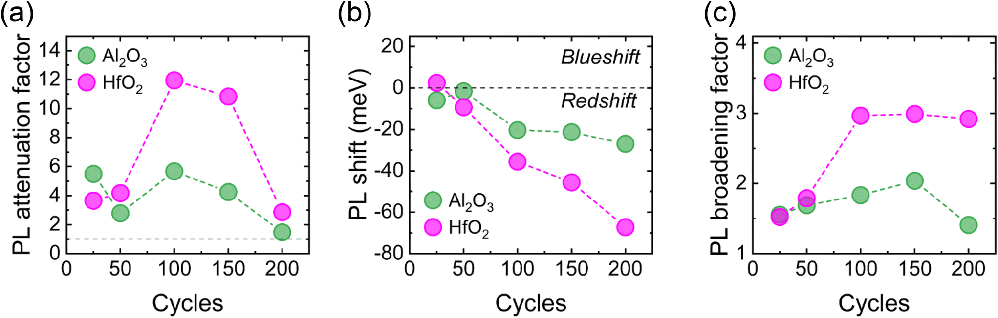 | ||
| Fig. 5 Comparison of average (a) PL attenuation factors, (b) shifts in PL energy, and (c) PL FWHM broadening factors extracted from the mapping data associated with ALD of Al2O3 (green) and HfO2 (magenta). | ||
We find non-monotonic relations between the number of ALD cycles and the degree of PL attenuation for both Al2O3 and HfO2. For each dielectric, the weakest reduction of the PL signal occurs after 200 ALD cycles, with 100 cycles yielding the largest attenuation. Generally, a greater number of ALD cycles of either dielectric gave rise to a larger redshift in the energy of the PL emission, with minor shifts (<6 meV) seen at low cycle numbers. Averaged across the mapping data, 25 ALD cycles of HfO2 resulted in a small blueshift in the PL energy. However, this blueshift may arise from the scatter in the data and, since it is <2 meV, we consider the shift negligible. For more than 50 ALD cycles, the redshift due to ALD-HfO2 is greater than that induced by ALD-Al2O3: following 200 ALD cycles of HfO2, the peak PL energy is downshifted by ∼65 meV, with only a ∼25 meV shift after 200 cycles of Al2O3. For ALD of Al2O3, the broadening of the MoS2 PL signal increased with the number of ALD cycles up to 150 cycles, where the deposition broadened the PL linewidth by a factor of ∼2. At 200 cycles, ALD of Al2O3 induced a broadening factor of only ∼1.4. For ALD of HfO2, the PL broadening factor increased up to 100 cycles before remaining constant at ∼3× for further cycles.
The attenuated intensity, downshifted energy, and broadened spectral width of the 1L MoS2 PL emission observed here following ALD of a dielectric material is consistent with previous reports, and such modification of the PL character is thought to originate from the introduction of defects and n-type doping.26,64–66 A variety of defect states can be created in 1L MoS2 during thermal ALD of high-κ dielectrics, including sulfur vacancies,67 charged defects at the dielectric/MoS2 interface,68,69 and oxygen substitution at sulfur sites due to exposure to oxidising co-reactants.33,39 Such defects in 1L MoS2 act as non-radiative recombination centres and reduce the PL signal strength by trapping photoexcited excitons in mid-bandgap states, thus inhibiting their radiative decay.70 The creation of defect states can also increase electron–phonon interactions, with the increased disorder in the 1L MoS2 crystal structure broadening the PL linewidth.71,72 Since deconvolution of the PL emission can reveal information on both the prevalence of defect states and the electron density in MoS2,73,74 we decompose each single-site PL spectrum obtained before and after ALD into three individual peaks: A and B exciton emissions and an A− trion feature. The full deconvoluted spectra associated with the ALD of Al2O3 and HfO2 performed in this study are provided in Fig. S8 and S9 in the ESI,† respectively. The ratio of the absolute intensity of the B excitonic PL feature to that of the A exciton has been proposed by McCreary et al. as an indicator of defect density in MoS2, with a larger ratio corresponding to a more significant abundance of defect states.73 Since we employ a three-peak fitting of the PL spectra, we define an excitonic ratio as B/(A + A−), and the increase in this ratio is plotted as a function of ALD cycle number for both Al2O3 and HfO2 in Fig. 4c. ALD of each dielectric increases the B/(A + A−) ratio at all ALD cycle numbers, indicating each deposition introduces defect states in 1L MoS2. The trends in the increase in B/(A + A−) ratio for each dielectric (Fig. 4c) generally follow the same trajectory as those of the corresponding PL attenuation factor (Fig. 5a), suggesting defect formation is a primary source of dielectric-induced reduction of the 1L MoS2 PL signal. The maximum increase in B/(A + A−) ratio for ALD of both dielectrics occurs at 100 ALD cycles. Beyond 100 cycles, the increase in B/(A + A−) ratio becomes less significant as the surface coverage of the dielectric film increases, and fewer additional defects are created in 1L MoS2, particularly at 200 cycles. In general, the change in B/(A + A−) ratio induced by ALD of Al2O3 is greater than that following ALD of HfO2. We speculate that the enhanced defect formation during Al2O3 deposition may be due to the lateral expansion of islands that does not occur during HfO2 growth.
In addition to defect generation, n-type doping can also contribute to a reduced, redshifted, and broadened MoS2 PL signal.64,74 ALD-grown high-κ dielectrics can modify the electron density in MoS2via charge transfer at the interface.39,65,69,75,76 Since the formation of A− trions is encouraged by an excess of electrons,77 the ratio of the absolute intensity of the trionic component to that of the A excitonic feature, A−/A, can serve as an indicator of the electron density in MoS2.78Fig. 4d presents evolution of the A−/A ratio with the number of ALD cycles for the growth of Al2O3 and HfO2. We find that ALD of each dielectric increases the A−/A ratio to some extent at all number of ALD cycles, indicating n-type doping of 1L MoS2. The enhancement of the A−/A ratio increases from 25 to 100 ALD cycles for both dielectrics, before stabilising after 100 cycles. Since the n-type doping of MoS2 is known to proceed via an interfacial transfer of electron density, we suggest that this trend can be attributed to an increase in the number of interfacial sites as further dielectric material is deposited. After 100 cycles, the increased surface coverage of both dielectric films may mean that many interfacial sites are occupied, and further interfacial charge transfer at higher ALD cycle numbers is minimal. The similar magnitude of the increase in A−/A ratio for both ALD-Al2O3 and HfO2 at each number of cycles suggests film thickness is not a critical factor in the charge transfer, consistent with an interfacial interaction. In addition to increases in the A−/A ratio, the overall progressive redshift of the MoS2 PL signal observed for increasing ALD cycles of Al2O3 and HfO2 may be attributed in part to an increasing redshift in the energy of the A− contribution, as shown in Fig. S10 in the ESI.† Despite an apparent general relation between surface coverage and increase in A−/A ratio, this intensity ratio may also be impacted by strain and dielectric screening effects. Increasing the dielectric environment of 1L MoS2 has been reported to enhance and blueshift the PL emission.78 Since we observe PL attenuation and redshift following all depositions of Al2O3 and HfO2, we exclude any significant dielectric screening effects. We develop a clearer understanding of the dielectric-induced strain and doping of 1L MoS2 in the subsequent analysis of the Raman emission.
The distinct Raman spectrum of 1L MoS2 comprises two characteristic peaks: an in-plane E12g vibration at ∼384 cm−1 that is sensitive to strain and an out-of-plane A1g mode at ∼403 cm−1 that is responsive to charge doping.79,80 We obtained single-site Raman spectra and spatially resolved maps of the positions and linewidths of the E12g and A1g peaks before and after each ALD of Al2O3 or HfO2, and these are provided in section S7 of the ESI.† For growth of Al2O3 and HfO2, we observe small but appreciable widening of the FWHM of the 1L MoS2 Raman peaks at all ALD cycle numbers, with a general increase in the degree of broadening as the cycle number increases (see Fig. S16 in the ESI†). Broadening of the characteristic MoS2 Raman modes indicates enhanced phonon scattering, typically associated with increased disorder that may arise from the introduction of strain or charge doping.81 To quantitatively separate the changes in electron density, n, and mechanical strain, ε, in CVD-1L MoS2 induced by each deposition, we employ a correlative analysis previously applied to graphene82–84 and MoS2.26,37,85–88Details of this procedure can be found in section S8 of the ESI.†Fig. 6 presents correlative plots of A1g peak position as a function of E12g wavenumber extracted from the Raman mapping data, with overlayed ε–n grids, for each ALD process studied here. The red dashed lines correspond to doping isolines and represent Δn = ±0.1 × 1013 cm−2 relative changes in the electron density. A positive (negative) Δn indicates n-type (p-type) doping. Strain isolines are indicated by the black dashed lines and demonstrate variations in the strain of Δε = ±0.1%. Δε > 0 corresponds to tensile strain, with Δε < 0 representing compressive strain. Comparisons of the doping and strain induced in 1L MoS2 by ALD of Al2O3 and HfO2 at each number of ALD cycles are given in Fig. 6c and d, respectively.
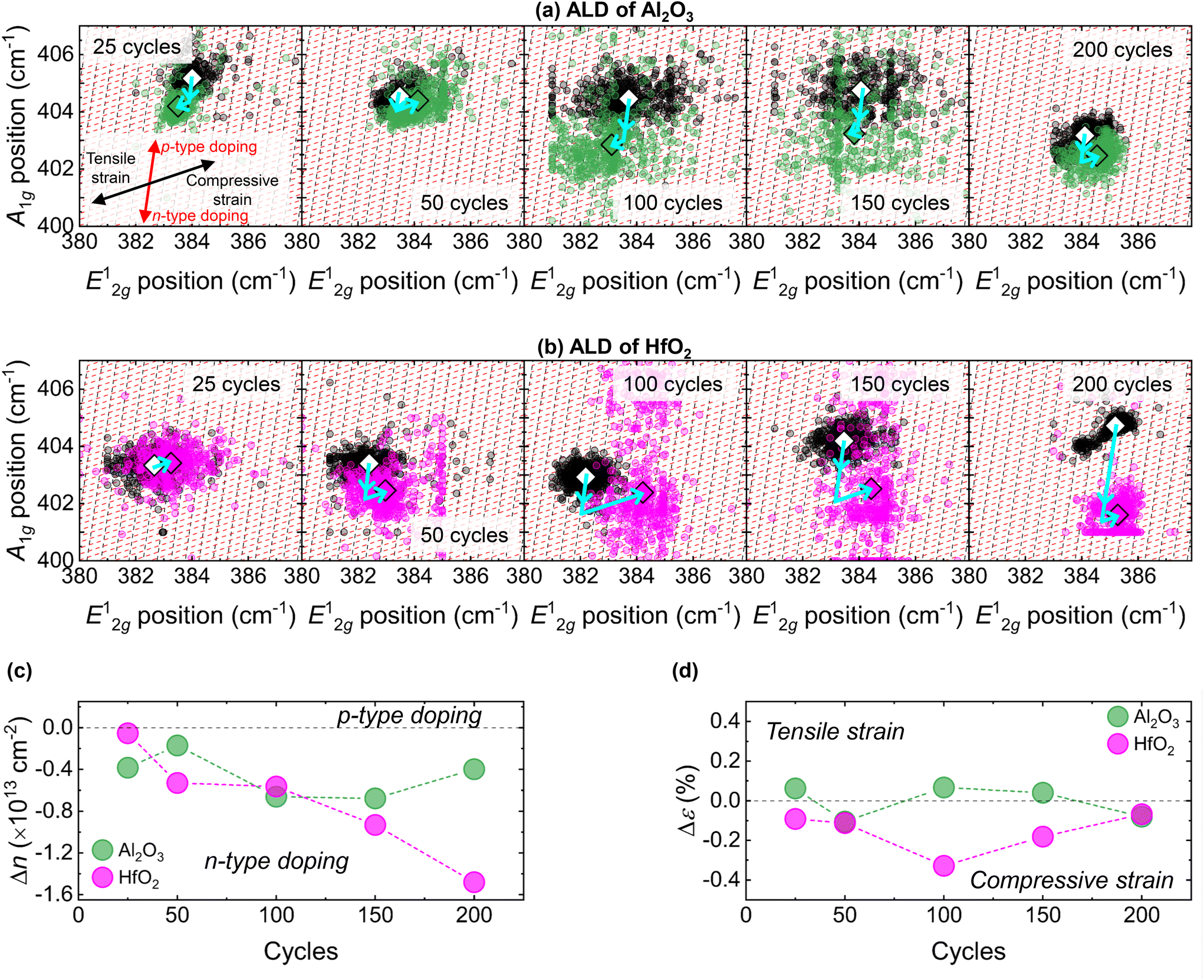 | ||
| Fig. 6 Correlative plots of A1g and E12g peak positions extracted from Raman mapping data before (black/white) and after ALD of (a) Al2O3 (green) and (b) HfO2 (magenta) at each number of ALD cycles. The small circular translucent markers arise from every pixel extracted from the Raman mapping data and the large diamond points indicate the corresponding average values. Strain isolines (black dashed lines) indicate Δε = ±0.1% variations in the strain and doping isolines (red dashed lines) correspond to relative changes in the electron density of Δn = ±0.1 × 1013 cm−2. The directions of the strain and doping effects are highlighted in the first panel. Comparison of the average relative changes in (c) electron density, Δn, and (d) mechanical biaxial strain, Δε, for each deposition. | ||
From analysis of the Raman maps, we find thermal ALD of Al2O3 or HfO2 induces some degree of n-type doping in CVD-1L MoS2 at all number of cycles, in good agreement with the general changes to the A−/A ratio extracted from the single-site PL data. We estimate that 25 cycles of ALD-Al2O3 enhances the MoS2 electron density by ∼0.4 × 1013 cm−2, yet only a ∼0.2 × 1013 cm−2 increase results from 50 ALD cycles. The degree of Al2O3-induced n-type doping reaches a maximum at 100 cycles and 150 cycles, with the electron density of 1L MoS2 increased by ∼0.7 × 1013 cm−2 following both depositions. At 200 ALD cycles of Al2O3, the degree of n-type doping is only ∼0.4 × 1013 cm−2, comparable to that observed after 25 cycles, despite ∼85% surface coverage. The variation in the extent of n-type doping of 1L MoS2 following ALD of Al2O3 is well explained by the saturation of interfacial sites at increased surface coverage. Due to the lateral component of the 3D growth mode, further Al2O3 film growth after 100 ALD cycles occurs primarily on existing islands rather than directly on uncovered MoS2, limiting further charge transfer. For ALD of HfO2 on CVD-1L MoS2, the degree of n-type doping increases monotonically with cycle number up to 200 cycles. With minimal change in the electron density observed after 25 cycles of ALD-HfO2, the increase in electron density in 1L MoS2 is ∼1.5 × 1013 cm−2 after 200 cycles. As the charge transfer occurs at the interfacial region between the ALD-dielectric and 1L MoS2 surface, the enhanced degree of n-type doping at higher ALD cycle numbers can be explained by the increasing surface coverage and lack of lateral expansion of HfO2 islands. In addition, a greater doping effect is seen for HfO2 at higher cycle numbers, where significant dielectric film coalescence is observed. This can be attributed to the higher dielectric constant of HfO2: the dielectric constants of Al2O3 and HfO2 are ∼8.5 and ∼20, respectively.89,90 High-κ dielectrics alter the local electric field on the MoS2 surface, thus encouraging electron accumulation at the interface. A higher dielectric constant ALD-film will facilitate stronger interfacial electrostatic interactions and more efficient charge transfer. Moreover, ALD-HfO2 films are more likely to exhibit oxygen deficiency due to a tendency to form sub-stoichiometric HfOx phases, further contributing to n-type doping effects.39
The induced changes to strain in 1L MoS2 due to ALD of Al2O3 are relatively small (|Δε| < 0.2%). The varying degrees of compressive or tensile strain are likely a result of local fluctuations due to the island morphologies and incomplete coalescence of the ALD-Al2O3 films. In contrast, only compressive strain was introduced in 1L MoS2 following ALD of HfO2. A maximum compressive strain (Δε ∼−0.3%) was imparted on MoS2 after 100 cycles of HfO2 and we suggest that this is due to localised strain effects from the vertically developing island features. Beyond 100 ALD cycles of HfO2, the film coalescence increases such that the strain imparted on the underlying MoS2 is distributed more evenly and a progressively weaker overall compressive strain effect is seen. We speculate that the relatively modest strain effects observed here in 1L MoS2 following ALD of Al2O3 or HfO2 are a result of the physisorption-driven nature of the film nucleation. The resulting vdW interaction between the dielectric and the underlying 1L MoS2 may limit the efficient transfer of mechanical strain into the monolayer. An exact understanding of the strain effects induced in CVD-1L MoS2 during ALD of high-κ dielectrics requires further research attention.
Conclusions
We have systematically studied the nucleation and growth of Al2O3 and HfO2 films deposited directly on CVD-1L MoS2via thermal ALD at 200 °C. We have revealed ALD-Al2O3 films develop via 3D island growth, with estimated vertical and lateral GPCs of 0.09 ± 0.01 nm and 0.06 ± 0.01 nm, respectively. We find ALD-HfO2 films also exhibit island morphology, but the absence of lateral expansion indicates the growth of HfO2 does not evolve via the same 3D mode. We attribute the differing growth mechanisms to variations in precursor/1L MoS2 interactions and nucleation kinetics. We have also investigated the change in the optical behaviour of 1L MoS2 with differing numbers of ALD cycles of Al2O3 and HfO2. We find that ALD of Al2O3 and HfO2 both induce some degree of PL attenuation, redshift, and broadening at all cycle numbers, consistent with defect generation and n-type doping. We connect the modified optical properties of encapsulated 1L MoS2 to the surface coverage and morphology of the ALD-dielectric films, and rationalise the extent of n-type doping in terms of interfacial charge transfer. This study of the direct ALD of high-κ dielectric materials on CVD-1L MoS2 films has revealed nucleation and growth behaviours that are important for the realisation of 1L MoS2-based device structures.Author contributions
This study was conceptualised by B. F. M. H. Experimental work was primarily conducted by B. F. M. H., with support from S. L. P. Data analysis was largely performed by B. F. M. H., with discussions and contributions from S. L. P., N. E. G., and J. D. M. The manuscript was written by B. F. M. H., with input and editing from S. L. P., N. E. G., and J. D. M.Data availability
Data underpinning figures in this paper can be freely downloaded from https://wrap.warwick.ac.uk/191653/. Requests for additional data should be made directly to the corresponding author.Conflicts of interest
There are no conflicts to declare.Acknowledgements
The authors acknowledge use of Raman/PL facilities within the Spectroscopy Research Technology Platform (RTP), University of Warwick, the AFM facilities within the Electron Microscopy RTP, University of Warwick, and the ALD facilities within the Nano Fabrication RTP, University of Warwick. The Spectroscopy and Electron Microscopy RTPs are part of the Warwick Analytical Science Centre supported by EPSRC (EP/V007688/1). S. L. P. is supported by a Royal Academy of Engineering Research Fellowship (RF-2324-23-197).References
- K. F. Mak, C. Lee, J. Hone, J. Shan and T. F. Heinz, Phys. Rev. Lett., 2010, 105, 136805 CrossRef PubMed
.
- A. Splendiani, L. Sun, Y. Zhang, T. Li, J. Kim, C.-Y. Chim, G. Galli and F. Wang, Nano Lett., 2010, 10, 1271–1275 CrossRef CAS PubMed
- Q. H. Wang, K. Kalantar-Zadeh, A. Kis, J. N. Coleman and M. S. Strano, Nat. Nanotechnol., 2012, 7, 699–712 CrossRef CAS PubMed
- N. Thomas, S. Mathew, K. M. Nair, K. O'Dowd, P. Forouzandeh, A. Goswami, G. McGranaghan and S. C. Pillai, Mater. Today Sustainability, 2021, 13, 100073 CrossRef
- J. Jeon, S. K. Jang, S. M. Jeon, G. Yoo, Y. H. Jang, J.-H. Park and S. Lee, Nanoscale, 2015, 7, 1688–1695 RSC
- B. Radisavljevic, A. Radenovic, J. Brivio, V. Giacometti and A. Kis, Nat. Nanotechnol., 2011, 6, 147–150 CrossRef CAS PubMed
- M. Fontana, T. Deppe, A. K. Boyd, M. Rinzan, A. Y. Liu, M. Paranjape and P. Barbara, Sci. Rep., 2013, 3, 1634 CrossRef PubMed
- A. Pospischil, M. M. Furchi and T. Mueller, Nat. Nanotechnol., 2014, 9, 257–261 CrossRef CAS PubMed
- M. M. Furchi, A. Pospischil, F. Libisch, J. Burgdörfer and T. Mueller, Nano Lett., 2014, 14, 4785–4791 CrossRef CAS PubMed
- Y. Zhang, H. Li, L. Wang, H. Wang, X. Xie, S.-L. Zhang, R. Liu and Z.-J. Qiu, Sci. Rep., 2015, 5, 7938 CrossRef CAS PubMed
- O. Lopez-Sanchez, D. Lembke, M. Kayci, A. Radenovic and A. Kis, Nat. Nanotechnol., 2013, 8, 497–501 CrossRef CAS PubMed
- M. Nayeri, M. Moradinasab and M. Fathipour, Semicond. Sci. Technol., 2018, 33, 025002 CrossRef
- Y. Zhang, J. Ye, Y. Matsuhashi and Y. Iwasa, Nano Lett., 2012, 12, 1136–1140 CrossRef CAS PubMed
- N. Aspiotis, K. Morgan, B. März, K. Müller-Caspary, M. Ebert, E. Weatherby, M. E. Light, C.-C. Huang, D. W. Hewak, S. Majumdar and I. Zeimpekis, npj 2D Mater. Appl., 2023, 7, 18 CrossRef CAS
- C. Liu, H. Chen, S. Wang, Q. Liu, Y.-G. Jiang, D. W. Zhang, M. Liu and P. Zhou, Nat. Nanotechnol., 2020, 15, 545–557 CrossRef CAS PubMed
- S. M. George, Chem. Rev., 2010, 110, 111–131 CrossRef CAS PubMed
- R. W. Johnson, A. Hultqvist and S. F. Bent, Mater. Today, 2014, 17, 236–246 CrossRef CAS
- D. J. Hagen, M. E. Pemble and M. Karppinen, Appl. Phys. Rev., 2019, 6, 041309 Search PubMed
- R. S. Bonilla, B. Hoex, P. Hamer and P. R. Wilshaw, Phys. Status Solidi A, 2017, 214, 1700293 CrossRef
- M. Leskelä and M. Ritala, Angew. Chem., Int. Ed., 2003, 42, 5548–5554 CrossRef PubMed
- M. Chhowalla, H. S. Shin, G. Eda, L.-J. Li, K. P. Loh and H. Zhang, Nat. Chem., 2013, 5, 263–275 CrossRef PubMed
- H. Liu, K. Xu, X. Zhang and P. D. Ye, Appl. Phys. Lett., 2012, 100, 152115 CrossRef
- B. J. Chou, Y. C. Chang, W. H. Chang and C. H. Chen, IEEE J. Electron Devices Soc., 2022, 10, 1033–1039 CAS
- J. Yang, S. Kim, W. Choi, S. H. Park, Y. Jung, M.-H. Cho and H. Kim, ACS Appl. Mater. Interfaces, 2013, 5, 4739–4744 CrossRef CAS PubMed
- S. McDonnell, B. Brennan, A. Azcatl, N. Lu, H. Dong, C. Buie, J. Kim, C. L. Hinkle, M. J. Kim and R. M. Wallace, ACS Nano, 2013, 7, 10354–10361 CrossRef CAS PubMed
- B. F. M. Healy, S. L. Pain, J. Lloyd-Hughes, N. E. Grant and J. D. Murphy, Adv. Mater. Interfaces, 2024, 11, 2400305 CrossRef CAS
- S. Son, S. Yu, M. Choi, D. Kim and C. Choi, Appl. Phys. Lett., 2015, 106, 021601 CrossRef
- X. Zou, J. Wang, C.-H. Chiu, Y. Wu, X. Xiao, C. Jiang, W.-W. Wu, L. Mai, T. Chen, J. Li, J. C. Ho and L. Liao, Adv. Mater., 2014, 26, 6255–6261 CrossRef CAS PubMed
- B. Huang, M. Zheng, Y. Zhao, J. Wu and J. T. L. Thong, ACS Appl. Mater. Interfaces, 2019, 11, 35438–35443 CrossRef CAS PubMed
- C. Jung, H. I. Yang and W. Choi, Nanoscale Res. Lett., 2019, 14, 278 CrossRef PubMed
- S. Park, S. Y. Kim, Y. Choi, M. Kim, H. Shin, J. Kim and W. Choi, ACS Appl. Mater. Interfaces, 2016, 8, 11189–11193 CrossRef CAS PubMed
- A. Azcatl, S. McDonnell, S. K. C. X. Peng, H. Dong, X. Qin, R. Addou, G. I. Mordi, N. Lu, J. Kim, M. J. Kim, K. Cho and R. M. Wallace, Appl. Phys. Lett., 2014, 104, 111601 CrossRef
- B. F. M. Healy, S. L. Pain, M. Walker, N. E. Grant and J. D. Murphy, ACS Appl. Nano Mater., 2025, 8, 7334–7346 CrossRef CAS PubMed
- A. Hiraiwa, D. Matsumura and H. Kawarada, J. Appl. Phys., 2016, 120, 084504 CrossRef
- H. Zhang, D. Chiappe, J. Meersschaut, T. Conard, A. Franquet, T. Nuytten, M. Mannarino, I. Radu, W. Vandervorst and A. Delabie, J. Chem. Phys., 2016, 146, 052810 CrossRef PubMed
- K. M. Price, K. E. Schauble, F. A. McGuire, D. B. Farmer and A. D. Franklin, ACS Appl. Mater. Interfaces, 2017, 9, 23072–23080 CrossRef CAS PubMed
- E. Schilirò, S. E. Panasci, A. M. Mio, G. Nicotra, S. Agnello, B. Pecz, G. Z. Radnoczi, I. Deretzis, A. La Magna, F. Roccaforte, R. Lo Nigro and F. Giannazzo, Appl. Surf. Sci., 2023, 630, 157476 CrossRef
- J. A. Kropp, Y. Cai, Z. Yao, W. Zhu and T. Gougousi, J. Vac. Sci. Technol., A, 2018, 36, 06A101 CrossRef
- R. Mahlouji, Y. Zhang, M. A. Verheijen, S. Karwal, J. P. Hofmann, W. M. M. Kessels and A. A. Bol, ACS Appl. Nano Mater., 2024, 7, 18786–18800 CrossRef CAS PubMed
- E. Schilirò, R. Lo Nigro, F. Roccaforte and F. Giannazzo, Appl. Sci., 2021, 11, 11052 CrossRef
- T.-T. Lee, K. Chiranjeevulu, S. Pedaballi, D. Cott, A. Delabie, C.-F. Dee and E. Y. Chang, J. Vac. Sci. Technol., A, 2022, 41, 013201 CrossRef
- Y.-H. Lee, X.-Q. Zhang, W. Zhang, M.-T. Chang, C.-T. Lin, K.-D. Chang, Y.-C. Yu, J. T.-W. Wang, C.-S. Chang, L.-J. Li and T.-W. Lin, Adv. Mater., 2012, 24, 2320–2325 CrossRef CAS PubMed
- Y. Yu, C. Li, Y. Liu, L. Su, Y. Zhang and L. Cao, Sci. Rep., 2013, 3, 1866 CrossRef PubMed
- J. Zhang, H. Yu, W. Chen, X. Tian, D. Liu, M. Cheng, G. Xie, W. Yang, R. Yang, X. Bai, D. Shi and G. Zhang, ACS Nano, 2014, 8, 6024–6030 CrossRef CAS PubMed
- K. Kang, S. Xie, L. Huang, Y. Han, P. Y. Huang, K. F. Mak, C.-J. Kim, D. Muller and J. Park, Nature, 2015, 520, 656–660 CrossRef CAS PubMed
- M. P. C. Taverne, X. Zheng, Y.-S. J. Chen, K. A. Morgan, L. Chen, N. M. Palakkool, D. Rezaie, H. Awachi, J. G. Rarity, D. W. Hewak, C.-C. Huang and Y.-L. D. Ho, ACS Appl. Opt. Mater., 2023, 1, 990–996 CrossRef CAS PubMed
- A. A. Wibowo, M. Tebyetekerwa, A. D. Bui, F. Kremer, S. Saji, Z. Yin, Y. Lu, D. Macdonald and H. T. Nguyen, ACS Appl. Electron. Mater., 2022, 4, 5072–5080 CrossRef CAS
- J. You, M. D. Hossain and Z. Luo, Nano Convergence, 2018, 5, 26 CrossRef PubMed
- J. Hong, Z. Hu, M. Probert, K. Li, D. Lv, X. Yang, L. Gu, N. Mao, Q. Feng, L. Xie, J. Zhang, D. Wu, Z. Zhang, C. Jin, W. Ji, X. Zhang, J. Yuan and Z. Zhang, Nat. Commun., 2015, 6, 6293 CrossRef CAS PubMed
- W. Zhou, X. Zou, S. Najmaei, Z. Liu, Y. Shi, J. Kong, J. Lou, P. M. Ajayan, B. I. Yakobson and J.-C. Idrobo, Nano Lett., 2013, 13, 2615–2622 CrossRef CAS PubMed
- J. Gao, B. Li, J. Tan, P. Chow, T.-M. Lu and N. Koratkar, ACS Nano, 2016, 10, 2628–2635 CrossRef CAS PubMed
- K. Xu, W. Sun, Y. Shao, F. Wei, X. Zhang, W. Wang and P. Li, Nanotechnol. Rev., 2018, 7, 605–621 CrossRef CAS
- D. Nečas and P. Klapetek, Open Phys., 2012, 10, 181–188 CrossRef
- J. Schindelin, I. Arganda-Carreras, E. Frise, V. Kaynig, M. Longair, T. Pietzsch, S. Preibisch, C. Rueden, S. Saalfeld, B. Schmid, J.-Y. Tinevez, D. J. White, V. Hartenstein, K. Eliceiri, P. Tomancak and A. Cardona, Nat. Methods, 2012, 9, 676–682 CrossRef CAS PubMed
- L. G. A. Melo, A. P. Hitchcock, D. Susac, J. Stumper and V. Berejnov, Phys. Chem. Chem. Phys., 2018, 20, 16625–16640 RSC
-
Filmetrics Inc.
Operations Manual for the FILMETRICS F20 Thin-Film Analyzer, Filmetrics Inc., 7.3.2., 2013 Search PubMed
-
Filmetrics Inc.
Taking the Mystery Out of Thin-Film Measurement, Filmetrics Inc., 2012 Search PubMed
- T. Park, H. Kim, M. Leem, W. Ahn, S. Choi, J. Kim, J. Uh, K. Kwon, S.-J. Jeong, S. Park, Y. Kim and H. Kim, RSC Adv., 2017, 7, 884–889 RSC
- R. L. Puurunen and W. Vandervorst, J. Appl. Phys., 2004, 96, 7686–7695 CrossRef CAS
- I. Cho, J. Yang, S. S. Raya and B. Shong, Colloid Interface Sci. Commun., 2025, 65, 100823 CrossRef CAS
- B. F. M. Healy, S. L. Pain, J. Lloyd-Hughes, N. E. Grant and J. D. Murphy, Mater. Res. Express, 2024, 11, 015002 CrossRef CAS
- T. N. Walter, S. Lee, X. Zhang, M. Chubarov, J. M. Redwing, T. N. Jackson and S. E. Mohney, Appl. Surf. Sci., 2019, 480, 43–51 CrossRef CAS
- S. L. Pain, E. Khorani, A. Yadav, T. Niewelt, A. Leimenstoll, B. F. M. Healy, M. Walker, D. Walker, N. E. Grant and J. D. Murphy, RSC Appl. Interfaces, 2024, 1, 471–482 RSC
- Y. Li, X. Li, H. Chen, J. Shi, Q. Shang, S. Zhang, X. Qiu, Z. Liu, Q. Zhang, H. Xu, W. Liu, X. Liu and Y. Liu, ACS Appl. Mater. Interfaces, 2017, 9, 27402–27408 CrossRef CAS PubMed
- S. Y. Kim, H. I. Yang and W. Choi, Appl. Phys. Lett., 2018, 113, 133104 CrossRef
- M. Turunen, H. Fernandez, S.-T. Akkanen, H. Seppänen and Z. Sun, 2D Mater., 2023, 10, 045018 CrossRef CAS
- H. Jung, M. Kim, Y. Lee, G. B. Sim, H. Gu, S. Hong, S. Lee, J. Lee, D. Lee, T. Zou, K. Kang, C. W. Myung, Y.-Y. Noh and J. Kwon, ACS Nano, 2025, 19, 6069–6078 CrossRef CAS PubMed
- S. Kc, R. C. Longo, R. M. Wallace and K. Cho, ACS Omega, 2017, 2, 2827–2834 CrossRef CAS PubMed
- C. J. McClellan, E. Yalon, K. K. H. Smithe, S. V. Suryavanshi and E. Pop, ACS Nano, 2021, 15, 1587–1596 CrossRef CAS PubMed
- H. Wang, C. Zhang and F. Rana, Nano Lett., 2015, 15, 339–345 CrossRef CAS PubMed
- F. Mujeeb, V. Mahamiya, A. Singh, M. Kothari, A. Chowdhury, A. Shukla and S. Dhar, Appl. Phys. Lett., 2024, 125, 213103 CrossRef CAS
- F. Cadiz, E. Courtade, C. Robert, G. Wang, Y. Shen, H. Cai, T. Taniguchi, K. Watanabe, H. Carrere, D. Lagarde, M. Manca, T. Amand, P. Renucci, S. Tongay, X. Marie and B. Urbaszek, Phys. Rev. X, 2017, 7, 021026 Search PubMed
- K. M. McCreary, A. T. Hanbicki, S. V. Sivaram and B. T. Jonker, APL Mater., 2018, 6, 111106 CrossRef
- S. Mouri, Y. Miyauchi and K. Matsuda, Nano Lett., 2013, 13, 5944–5948 CrossRef CAS PubMed
- X. Zhang, Z. Shao, X. Zhang, Y. He and J. Jie, Adv. Mater., 2016, 28, 10409–10442 CrossRef CAS PubMed
- A. Henning, S. Levashov, C. Qian, T. Grünleitner, J. Primbs, J. J. Finley and I. D. Sharp, Adv. Mater. Interfaces, 2023, 10, 2202429 CrossRef CAS
- K. F. Mak, K. He, C. Lee, G. H. Lee, J. Hone, T. F. Heinz and J. Shan, Nat. Mater., 2013, 12, 207–211 CrossRef CAS PubMed
- Y. Lin, X. Ling, L. Yu, S. Huang, A. L. Hsu, Y.-H. Lee, J. Kong, M. S. Dresselhaus and T. Palacios, Nano Lett., 2014, 14, 5569–5576 CrossRef CAS PubMed
- X. Zhang, X.-F. Qiao, W. Shi, J.-B. Wu, D.-S. Jiang and P.-H. Tan, Chem. Soc. Rev., 2015, 44, 2757–2785 RSC
- H.-J. Kim, D. Kim, S. Jung, M.-H. Bae, Y. J. Yun, S. N. Yi, J.-S. Yu, J.-H. Kim and D. H. Ha, J. Raman Spectrosc., 2018, 49, 1938–1944 CrossRef CAS
- B. Chakraborty, A. Bera, D. V. S. Muthu, S. Bhowmick, U. V. Waghmare and A. K. Sood, Phys. Rev. B:Condens. Matter Mater. Phys., 2012, 85, 161403 CrossRef
- T. M. G. Mohiuddin, A. Lombardo, R. R. Nair, A. Bonetti, G. Savini, R. Jalil, N. Bonini, D. M. Basko, C. Galiotis, N. Marzari, K. S. Novoselov, A. K. Geim and A. C. Ferrari, Phys. Rev. B:Condens. Matter Mater. Phys., 2009, 79, 205433 CrossRef
- J. E. Lee, G. Ahn, J. Shim, Y. S. Lee and S. Ryu, Nat. Commun., 2012, 3, 1024 CrossRef PubMed
- E. Schilirò, R. Lo Nigro, S. E. Panasci, F. M. Gelardi, S. Agnello, R. Yakimova, F. Roccaforte and F. Giannazzo, Carbon, 2020, 169, 172–181 CrossRef
- A. Michail, N. Delikoukos, J. Parthenios, C. Galiotis and K. Papagelis, Appl. Phys. Lett., 2016, 108, 173102 CrossRef
- W. H. Chae, J. D. Cain, E. D. Hanson, A. A. Murthy and V. P. Dravid, Appl.
Phys. Lett., 2017, 111, 143106 CrossRef
- S. E. Panasci, E. Schilirò, G. Greco, M. Cannas, F. M. Gelardi, S. Agnello, F. Roccaforte and F. Giannazzo, ACS Appl. Mater. Interfaces, 2021, 13, 31248–31259 CrossRef CAS PubMed
- E. Schilirò, R. L. Nigro, S. E. Panasci, S. Agnello, M. Cannas, F. M. Gelardi, F. Roccaforte and F. Giannazzo, Adv. Mater. Interfaces, 2021, 8, 2101117 CrossRef
- Y. Lu, S. Bangsaruntip, X. Wang, L. Zhang, Y. Nishi and H. Dai, J. Am. Chem. Soc., 2006, 128, 3518–3519 CrossRef CAS PubMed
- M. D. Groner, F. H. Fabreguette, J. W. Elam and S. M. George, Chem. Mater., 2004, 16, 639–645 CrossRef CAS
Footnote |
| † Electronic supplementary information (ESI) available: Characterisation of 1L MoS2, further AFM images of ALD-Al2O3 and -HfO2 films, evaluation of island height in ALD-Al2O3 film after 200 cycles, estimation of ALD-HfO2 thickness on 1L MoS2, PL mapping data, deconvoluted single-spot PL spectra, single-spot and mapping Raman data, and correlative analysis of strain and doping in 1L MoS2. See DOI: https://doi.org/10.1039/d5nr01144b |
| This journal is © The Royal Society of Chemistry 2025 |