
 Open Access Article
 This Open Access Article is licensed under a Creative Commons Attribution-Non Commercial 3.0 Unported Licence
Unveiling of free carrier transport and ion migration in a 2D–3D perovskite mixture for stable optoelectronic devices†
Bich Phuong
Nguyen
a,
Sarah Su-O
Youn
b,
Yeon Soo
Kim
a,
Thuy Thi
Nguyen
a,
Ha Kyung
Park
b,
Gee Yeong
Kim
c and
William
Jo
 *ab
*ab
aNew and Renewable Energy Research Center (NREC), Ewha Womans University, Seoul 03760, Republic of Korea. E-mail: wmjo@ewha.ac.kr
bDepartment of Physics, Ewha Womans University, Seoul 03760, Republic of Korea
cAdvanced Photovoltaics Research Center, Korea Institute of Science and Technology (KIST), Seoul 02792, Republic of Korea
First published on 28th May 2025
Abstract
Manipulating charge carrier recombination dynamics in mixed three-dimensional (3D) and two-dimensional (2D) perovskites is an effective approach to enhance performance and long-term stability in both solar cells and light-emitting diodes (LEDs). Due to high crystallinity and a low charge carrier recombination coefficient, photogenerated charge carriers in solar cells can effectively diffuse across the perovskite layer, while enhancing radiative recombination through charge carrier confinement can significantly improve electroluminescence efficiencies in LEDs. Further improvements in device efficiency and stability require a comprehensive understanding of charge carrier transport at the numerous interfaces between the different phases of 2D perovskites at both the micro- and nanoscale, as well as ion migration. In this study, we examine the carrier transport mechanism at the thin-surface 2D/bulk 3D perovskite interface and the dense-surface 2D/3D heterophase. The electrical properties and ion migration behavior were analyzed by examining the transition of the J–V characteristics in both vertical and lateral devices. We carefully analyzed the influence of nanostructures on charge transport using conductive atomic force microscopy (C-AFM) and Kelvin probe force microscopy (KPFM). The variation in the spatial response of the photocurrent and surface photovoltage across grains and grain boundaries with different phases of the 2D perovskite was carefully examined. These insights provide a pathway for optimizing the electrical properties and charge transport behavior of mixed perovskites, further positioning them as key materials for the development of efficient and stable optoelectronic devices.
Introduction
Halide perovskite materials have enabled remarkable advancements in photovoltaics1–4 and light-emitting devices (LEDs).5–7 The conventional three-dimensional (3D) perovskites, represented by the general formula ABX3 (where A denotes the metal or organic cation, B represents a larger metal cation, and X indicates a halide anion), exhibit high charge mobilities, a large absorption coefficient, and a suitable bandgap, but typically demonstrate poor stability under ambient conditions and facilitate ion migration under optoelectrical fields.8 Compared to 3D perovskites, two-dimensional (2D) perovskites, represented by the general formula L2An−1BnX3n+1 (where L denotes the organic cation and n represents the number of inorganic layers within [BX6]4− octahedra), exhibit high photoluminescence quantum yield and long-term stability but low carrier mobilities.9,10 Thus, mixed-dimensional 2D–3D perovskites are proposed to combine the advantages of 2D and 3D perovskites, in which the 3D perovskite ensures effective optoelectronic properties and the 2D perovskite enhances the stability of optoelectronic devices. In photovoltaics, surface functionalization and interfacial modification using a large cation perovskite, such as phenethylammonium (PEA+ = C8H12N+) or butylammonium (BA+ = CH3(CH2)3NH3+), can interact with the inorganic octahedral layer, which will be able to passivate the surface defects in 3D perovskites.11–13 Additionally, residual stress relaxation leads to a uniform perovskite microstructure, reducing additional driving force for ion migration and improving the charge transport at the interface, thereby enhancing photovoltaic performance.14,15 However, the performance of mixed-dimensional 2D–3D perovskite solar cells does not break through the efficiency limit as expected due to the restricted charge transport at the mixed 2D–3D heterojunction interface. The effect of 2D perovskites on the 3D perovskites can effectively regulate the energy level alignment between the perovskite and the charge transport layer to improve the charge transport. However, these conflicting results have been attributed to the formation of either type-I or type-II band alignment for identical or similar cation species, leading to contradictory explanations for optoelectronic device performance. For example, the type-I alignment at the 2D–3D heterojunction interface leads to enhanced photovoltaic performance due to suppressed carrier recombination;12,16 however, reduced carrier extraction has also been observed owing to high photoexcitation transfer from the 2D to 3D perovskite phases.5,6,17 Similarly, Xiong et al. reported that fluctuations in type-II alignment acted as energy barriers to charge transfer, thereby decreasing performance.16 Conversely, improving charge carrier extraction enhances performance.18,19 One possibility may be related to variations in the phase distribution,20 orientation21 and the structure22–24 of large organic cations, which manipulate the quantum confinement effect and dielectric confinement effect. In LEDs, the excitons or charge carriers are confined within a potential well in the 2D perovskite, which facilitates fast radiative recombination and energy transfer between the 2D multiphases. Although well-confined charge carriers within 2D perovskites are beneficial for the photoluminescence (PL) and electroluminescence efficiencies of LEDs, this approach can pose a critical challenge to device stability. The numerous interfaces between the different phases of a 2D perovskite can create a high density of surface and interfacial defects. Although these defects may be electronically benign or inactive, they play a critical role in determining the environmental and operational stability of perovskites and optoelectronic devices. To gain in-depth insights into the properties of 2D–3D mixed perovskites, this study examined the electrical properties and carrier transport behaviors of (BA2PbI4)x(MAPbI3)1−x mixed perovskites with different 2D BA2PbI4 phases incorporated within 3D MAPbI3 (MA+ = CH3NH3+). Direct microscopic investigation of optoelectronic properties can enhance the understanding of the local properties of 2D–3D perovskites. The electrical properties of 2D–3D mixed perovskites were determined by measuring their J–V characteristics. Our results identified potential barriers and ideality factors that affect the charge transport in vertical devices owing to variations of the Fermi level (EF), charge concentration, and charge mobility. Furthermore, the ionic and electronic conductivities of the 2D–3D mixed perovskites based on the lateral devices were quantified through direct-current (DC) galvanostatic polarization measurements. Specifically, our in-depth analysis focused on the electrical properties and ion migration at the nanoscopic scale using Kelvin probe force microscopy (KPFM) and conductive atomic force microscopy (C-AFM). We observed that the 2D–3D films exhibit highly heterogeneous dynamics in response to photoexcitation across intra-grains (IGs) and grain boundaries (GBs). The average surface photovoltage sign is dominated by the band bending at the 2D–3D interfaces. Overall, our methodology is expected to pave the way for new theories that elucidate the role and contributions of large cations in optoelectronic devices.Experimental methods
Fabrication of 2D–3D perovskite thin films
1.5 M solution of the MAPbI3 precursor was first prepared by dissolving methylammonium iodide (MAI, Greatcell Solar) and lead iodide (PbI2, TCI) in anhydrous N,N-dimethylformamide (DMF, Sigma-Aldrich). The BA2PbI4 precursor was then prepared by dissolving n-butylammonium iodide (BAI, Greatcell Solar) and PbI2 in DMF. Both solutions were stirred overnight in a nitrogen-filled glovebox. The resulting MAPbI3 and BA2PbI4 precursor solutions were appropriately combined to obtain (BA2PbI4)x(MAPbI3)1−x samples with varying BA2PbI4 contents (x = 0.00, 0.02, 0.10, and 1.00). After blending, each sample solution was filtered and spin coated onto a substrate at 1000 rpm for 10 s and at 5000 rpm for 25 s. Chlorobenzene (acting as the antisolvent) was introduced during the second spin-coating step after 10 s. Subsequently, all samples were annealed on a hot plate at 100 °C for 15 min. Notably, the sample with the pure 2D perovskite phase was spin coated onto a substrate preheated at 80 °C.Film characterization
Activation energy measurements of the synthesized films were conducted in a Lakeshore Probe Station in a vacuum of 1.1 × 10⁻⁴ Pa. Here, temperature control was achieved using a heater and liquid He injection. During the activation energy measurements, the devices were first heated to 300 K for 15 min, following which they were cooled to target temperatures. Upon reaching each target temperature, the devices were allowed to stabilize for 5 min before current measurements were recorded. Standard probe-station analyses of the J–V characteristics were performed using a Keithley 4200-SCS, scanning over a voltage range of −0.5 to 1.2 V in increments of 10 mV, with a delay time of 1 ms. For ionic and electronic conductivity measurements, DC galvanostatic polarization experiments were conducted using a dual-channel model (Keithley model 2634b).The pure 3D MAPbI3, 2D–3D mixed, and pure 2D BA2PbI4 perovskite films were segmented into uniform square pieces (1 cm × 1 cm). Subsequently, 80 nm-thick gold electrodes were deposited onto the four corners of these pieces employing vacuum thermal deposition. Hall measurements were performed using HMS-3300/HT55T5.
The nanoscale conductive J–V characteristics of the films were assessed through C-AFM measurements conducted using a commercial AFM (n-Tracer, NanoFocus Inc.) equipped with a Pt/Ir cantilever (Nanosensors) under an air atmosphere. During these measurements, the imaging scan size was set to 3 × 3 μm2, the force constant was adjusted to 1 N m−1, and the scan speed was set to 0.5 Hz to reduce possible topography-induced artifacts. The tip of the AFM was grounded, while current measurements were conducted using a single terminal. Next, the surface potential distributions of the mixed 2D–3D perovskite films were examined using a KPFM (n-Tracer, NanoFocus Inc.), equipped with a Pt/Ir cantilever operating in the non-contact mode under an applied alternating current voltage of 1.0 V and frequency of 70 kHz. The work function of the tip was calibrated using a highly ordered pyrolytic graphite (HOPG) reference sample. During the calibration process, careful attention was paid to the stability of the tip to prevent any variations that could affect the measurements. In the KPFM measurements, the work function of the sample was determined from the contact potential difference (CPD) between the tip and the sample, as described by the following equation:
Additionally, the surface photovoltages (SPVs) of the films were measured using the KPFM assisted by perpendicular external laser dot modules with 640 nm wavelength at an intensity of 5 mW cm−2. Notably, the position of the external laser dot was adjusted to avoid interference with the built-in laser of the AFM. There is a minor topographic influence on potential imaging, typically arising from ‘cross-talk’ due to cantilever oscillations at the two frequencies used in AFM and KPFM measurements. To assess this effect, detailed line profiles were extracted in our previous study.11 Analysis of line profiles taken at multiple points across the surface revealed no correlation between variations in the work function and the surface topography. Consequently, no observable ‘cross-talk’ was found in the surface potential variations. A similar result was obtained in the C-AFM measurements.
Next, 2D grazing incidence wide-angle X-ray scattering (GIWAXS) patterns were recorded using a wide-angle X-ray scattering spectrometer (XEUSS 2.0, Xenocs) at the National Instrumentation Center for Environmental Management, Seoul National University. The X-ray wavelength was set to 1.54 Å, while the incidence angle was adjusted to 0.2°. Notably, the 2D GIWAXS data of the films were recorded using a DECTRIS hybrid pixel photon counting detector.
Furthermore, the surface of the perovskite films was analyzed by scanning electron microscopy (SEM) (Hitachi, SU8220, Korea Basic Science Institute) at an acceleration voltage of 5 kV and an applied current of 10 mA. Finally, the changes in chemical constituents and energy bands of the perovskite films were analysed using an ultraviolet photoemission spectroscopy (UPS) and X-ray photoelectron spectroscopy (XPS) measuring instrument (Axis Supra, Kratos, U.K.) at the National Center for Inter-University Research Facilities, Seoul National University. UPS was performed with a UV light source (He I, 21.22 eV) and XPS with a monochromatic microfocus X-ray source (Al Kα, 1486.7 eV).
Results and discussion
The evolution of phase composition and morphology in mixed 2D–3D perovskites has been studied for both photovoltaic and LED applications. According to our previous research, the original 2D perovskite (n = 1) phases demonstrate controlled growth within 3D perovskite matrices.11 As illustrated in the SEM images, the pure 3D perovskite film with relatively large grains contained many pinholes (Fig. 1a), which could limit the device's performance. In contrast, Fig. 1d shows that the pure 2D perovskite film exhibits a vertically aligned crystal arrangement. The 2D–3D mixed perovskite films, fabricated by adding 2D BA2PbI4 solutions at a molar ratio of 2 mol%, present reduced grain size and a flat surface and are free of pinholes, as illustrated in Fig. 1b. The added 2D perovskite impeded the growth of large 3D perovskite grains while preferentially occupying the GBs and surface.11,25,26 The corresponding sample is thus referred to as the 2D–3D passivation sample. However, with excessive 2D perovskite doping (10 mol%), an inhomogeneous surface with different grain sizes and segregation of the rod-like secondary phase are observed.27 Thus, the corresponding sample is termed the 2D–3D segregation sample (Fig. 1c).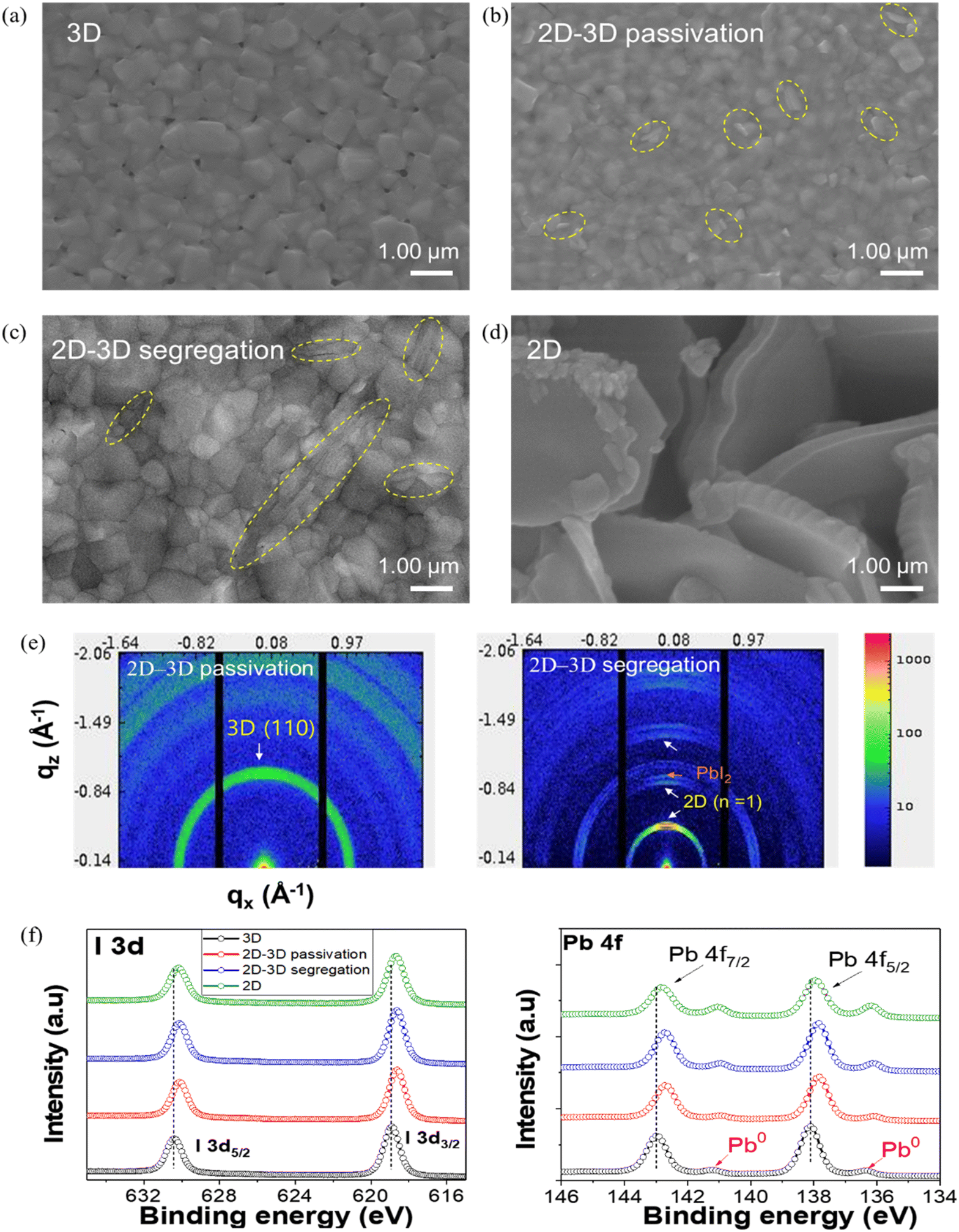 | ||
| Fig. 1 (a–d) Top-surface SEM images of the (BA2PbI4)x(MAPbI3)1−x perovskite films. Yellow-dashed ellipses indicate 2D perovskite platelets embedded within the 3D perovskite matrix. (e) GIWAXS images of 2D–3D passivation and segregation samples. (f) I 3d core level and Pb 4f core level XPS spectra of the (BA2PbI4)x(MAPbI3)1−x perovskite thin films. | ||
GIWAXS measurements were conducted to further examine the effects of 2D perovskites on the crystal orientation patterns of the 2D–3D mixed perovskites. As shown in Fig. S1,† the GIWAXS patterns exhibit typical scattering features of the 3D MAPbI3 perovskite, with a strong peak in the out-of-plane direction at qz = 1.00 Å, corresponding to the (110) plane. The GIWAXS patterns of the 2D–3D passivation sample evidently exhibit an intensification and sharpening of the diffraction ring compared to those of the pure 3D MAPbI3 perovskite, indicating the formation of preferentially oriented perovskite crystals with improved crystallinity (Fig. 1e). The highly oriented structure can be interpreted as a series of low-angle GBs arranged in the way that allows charge carriers to traverse the entire device more efficiently.11,12,28 However, the GIWAXS image of the 2D–3D passivation sample does not show clear patterns corresponding to the 2D BA2PbI4 perovskite due to its low content. In the case of the 2D–3D segregation sample, the intensity of the ring pattern associated with the 3D MAPbI3 perovskite is reduced, indicating altered crystallinity, while peaks corresponding to the secondary-phase 2D perovskite at qz = 0.45 Å and PbI2 = 0.90 Å become apparent. The formation of PbI2 could be attributed to the higher activation energy required to form the 2D perovskite compared to the 3D perovskite when the concentration of BA+ exceeds a certain threshold.11,26
Next, we subjected the (BA2PbI4)x(MAPbI3)1−x perovskite thin films to XPS measurements to gain structural insights (Fig. S2†). Notably, all spectra were calibrated against the C 1s peak located at approximately 284.8 eV (sp3 C–C bonding). As shown in Fig. 1f, the Pb 4f and I 3d core-level spectra of the 2D–3D mixed perovskite shift compared to those of the 3D perovskite. In particular, peaks corresponding to Pb 4f7/2 and Pb 4f5/2 shift to lower binding energies, indicating an increase in the electron cloud density surrounding Pb2+, which suggests that the BA cation can efficiently form a coordination bond with Pb2+.29 The I 3d spectra also exhibit similar behavior. In this case, the ammonium heads (NH+) of the BA cation form hydrogen bonds with both the bridging and terminal I atoms of the PbI64− octahedra, thereby affecting the bonding between NH+–I and Pb–I, respectively.29 However, compared to the Pb 4f and I 3d of the 2D–3D passivation sample, those of the 2D–3D segregation sample show no shifts, despite the increased 2D perovskite content. More importantly, the area occupied by peaks corresponding to metallic Pb0 within the Pb 4f spectrum decreases for the 2D–3D passivation sample, while it increases for the 2D–3D segregation sample, compared to the 3D perovskite (Fig. S2c†). The metallic Pb0 impurities are decomposition byproducts of residual PbI2 in perovskites under light or X-ray irradiation,3,30 indicating that the long Pb–I bonds in 2D perovskites are easily broken. This is consistent with the findings of Hu et al., who observed the easy degradation of 2D BA2PbI4 perovskites under X-ray irradiation and vacuum exposure.30
To gain insight into charge transport mechanisms in 2D–3D mixed perovskite systems, we investigated the spatial distribution of phases and the dynamics of interphase charge transfer. Perovskite/electrode contacts are crucial for the development of charge-transporting-layer-free devices, such as solar cells, field-effect transistors, artificial synapses, memory devices, and so on. Thus, elucidating the interfacial electronic structures and carrier behaviors of perovskite/metal junctions is fundamental to understanding and optimizing the performance of these devices. We further measured the J–V curves of the (BA2PbI4)x(MAPbI3)1−x perovskite thin films with a simple configuration Au/(BA2PbI4)x(MAPbI3)1−x/fluorine-doped tin oxide (FTO) vertical device under darkness (Fig. S3†). It can be observed that the J–V curves for 3D perovskites and 2D–3D mixed perovskites exhibit a half S-shape, whereas the J–V curve for 2D perovskites shows a linear dependence. Clearly, the MAPbI3/Au and MAPbI3/Au interfaces form a Schottky junction, while the BA2PbI4/Au and BA2PbI4/FTO interfaces form an ohmic junction. This discrepancy can be explained by the energy level alignment illustrated in Fig. 2a. The EF, valence band (EV), and conduction band (EC) were derived from the UPS results and optical bandgaps of the (BA2PbI4)x(MAPbI3)1−x perovskites (Fig. S4†).11 The calculated saturation current density (J0) and ideality factor (η) are shown in Fig. 2b. The lowest values of J0 (5.2 × 10⁻⁵ mA cm−2) and η (1.12) were observed in the 2D–3D passivation device, which suppresses carrier recombination. Moreover, current density in the 2D–3D passivation device showed a 1.5-fold increase in the forward region compared to that of the 3D device, due to the favorable energy band alignment in the 2D–3D passivation sample, which enhances efficient charge transport, particularly for electrons. In contrast to the 2D–3D segregation device, an increased current density under reverse bias was observed. The ideality factor (η > 2) confirmed that the leakage current mechanism is dominant, and the trap sites are present across the Schottky junction.
 | ||
| Fig. 2 (a) Schematic energy level diagrams of the (BA2PbI4)x(MAPbI3)1−x perovskite thin films. (b) Diode ideality factor and saturation current density of the (BA2PbI4)x(MAPbI3)1−x perovskite devices extracted from the analysis of dark J–V curves. The inset depicts the vertical device structure. (c) Carrier concentrations and Hall mobilities of (BA2PbI4)x(MAPbI3)1−x perovskite thin films. The inset depicts the schematic Hall measurement setup. (d and e) Dark J–V curves of the 2D–3D thin films with different phases deposited on the vertical structure, recorded at varying temperatures under a scan rate of 100 mV s−1 from −0.5 V to 1.2 V and back to −0.5 V. | ||
Fig. 2c depicts the variation in the carrier concentration and mobility of the 3D MAPbI3 perovskite film upon 2D BA2PbI4 doping using Hall measurement. In agreement with UPS measurements, the 3D MAPbI3 perovskite film exhibits n-type conduction with a high electron concentration of 9.61 × 1012 cm−3, while the 2D BA2PbI4 perovskite demonstrates p-type conduction. The 2D–3D mixed perovskites show more intrinsic behavior. For the 2D–3D passivation sample, the carrier concentration increases to 2.07 × 1013 cm−3, while mobility rises from 12 cm2 V−1 s−1 to 23 cm2 V−1 s−1 due to the lower defect state density. These increases in both carrier concentration and mobility lead to a corresponding enhancement in conductivity.11,31 However, with excess 2D perovskite doping, the mobility of the 2D–3D segregation sample decreased to 15 cm2 V−1 s−1, which can be attributed to the high density of defects and impurities. Li et al. explained that in the [CH3(CH2)n−1NH3]2PbI4 series, the in-plane mobility decreases with increasing alkyl chain length, accompanied by local deformation of the crystal lattice and distortions in the local chain structure.32
Our previous results revealed that varying amounts of 2D perovskites influence the performance and hysteresis behavior of the 2D–3D mixed perovskite solar cells.11 The migration of different ionic species within perovskite films affects the J–V hysteresis behavior, with the degree of hysteresis depending on the direction and temperature. Thus, to confirm the effects of 2D perovskites on the ion migration behavior of 2D–3D mixed perovskites, the J–V hysteresis loops of the samples were recorded at varying temperatures. At low temperatures, ions within the perovskite move slowly and are unable to follow the voltage scan, resulting in no hysteresis. However, as the temperature increases, these ions become more mobile, leading to an increase in hysteresis. In Fig. S5a,† the J–V hysteresis loops of the 3D MAPbI3 perovskite devices increase with rising temperature. This result confirms ion migration within 3D perovskite films, consistent with previous reports.33,34 In Fig. 2d, the J–V hysteresis loops of the 2D–3D passivation are minimal and do not change the shape as a function of temperature, indicating suppressed ion migration. This is because the long chain organic cations in 2D perovskites suppress ion migration.11,35 The shape of J–V curves of the 2D–3D segregation does not change, but the hysteresis loops increased compared to those of 2D–3D passivation (Fig. 2e). The electrical inhomogeneity analyzed in the C-AFM measurement below leads to a charge imbalance and increased charge accumulation at the multiphases due to their charge transporting abilities or trap charges at the defect sites. The charge transport behavior in 2D–3D mixed perovskites is critically linked to the performance of optoelectronic devices. Our group reported that a photovoltaic device incorporating a 2D molar ratio of 2% (passivation sample) achieved the highest power conversion efficiency of 15.17%, maintaining 80% of its initial efficiency after 45 days of storage in a desiccator at room temperature without encapsulation.11 In contrast, devices with a higher 2D molar ratio of 4% (segregation sample) exhibited notably diminished efficiency and stability over the same period. Furthermore, LED devices fabricated with a 2D![[thin space (1/6-em)]](https://www.rsc.org/images/entities/char_2009.gif) :3D (BAI:MAPbI3) molar ratio of 20:100 exhibited an increase in external quantum efficiency (EQE) from 1.00% to 10.40%, with no observable degradation after over 8 months of storage in a glovebox.27 Cho et al. reported that, without encapsulation, 2D–3D passivated perovskite photovoltaic devices exhibit a high efficiency of 21.7% and excellent moisture stability, retaining over 87% of their original performance after 38 days of storage in an ambient environment with 75 ± 20% relative humidity.36 This enhancement in moisture stability can be attributed to two main factors. First, the BA+ cation in the passivation interlayer has strong hydrophobic characteristics, which help prevent water molecules from penetrating the surface and reaching the underlying bulk perovskite through surface defects and GBs. Second, the improved surface coverage and morphology of the passivation layer further contribute to enhanced moisture stability.
:3D (BAI:MAPbI3) molar ratio of 20:100 exhibited an increase in external quantum efficiency (EQE) from 1.00% to 10.40%, with no observable degradation after over 8 months of storage in a glovebox.27 Cho et al. reported that, without encapsulation, 2D–3D passivated perovskite photovoltaic devices exhibit a high efficiency of 21.7% and excellent moisture stability, retaining over 87% of their original performance after 38 days of storage in an ambient environment with 75 ± 20% relative humidity.36 This enhancement in moisture stability can be attributed to two main factors. First, the BA+ cation in the passivation interlayer has strong hydrophobic characteristics, which help prevent water molecules from penetrating the surface and reaching the underlying bulk perovskite through surface defects and GBs. Second, the improved surface coverage and morphology of the passivation layer further contribute to enhanced moisture stability.
To confirm the hysteresis-suppressing effect of the 2D perovskite, we investigated the ion migration behavior of mixed (BA2PbI4)x(MAPbI3)1−x thin films, which were fabricated into Au/(BA2PbI4)x(MAPbI3)1−x/Au lateral conductor devices in the dark (Fig. 3a). The activation energies (Ea) of ion conductivity for the (BA2PbI4)x(MAPbI3)1−x perovskite films, which quantitatively characterize ion migration rates, were examined. Specifically, conductivity values at various temperatures were extracted from the J–V curves recorded under dark conditions and subsequently employed to calculate activation energies based on the following Nernst–Einstein relation:25
| σ(T) = (σ0/T)exp(−Ea/kT), | (1) |
 | ||
| Fig. 3 (a) Activation energies of the (BA2PbI4)x(MAPbI3)1–x perovskite thin films under dark conditions. The inset depicts the structure of the lateral device employed in activation energy measurement. (b) Electronic and ionic conductivities of the (BA2PbI4)x(MAPbI3)1–x perovskite thin films under dark and illuminated conditions. The inset depicts the interdigital electrode arrays of gold structure used in DC galvanostatic measurements. (c)–(d) Dark J–V curves of the 2D–3D thin films with different phases deposited on the interdigital electrode arrays of gold structure, recorded at a scan rate of 100 mV s−1 from 0.5 V to 0.5 V and back to 0.5 V. (e) Mixed electronic and ionic conduction in the 2D–3D thin films with different phases. | ||
As shown in Fig. S6,† the 3D MAPbI3 perovskite thin film exhibits two distinct slopes, likely corresponding to two different conduction mechanisms: electronic and ionic conduction. In the low-temperature range (200–240 K), ion motion is largely suppressed, and the conductivity is primarily governed by electronic conduction. Once the temperature exceeds 240 K, ionic conduction begins contributing to the electric current. This transition temperature from electronic to ionic conduction agrees well with the findings of a recent study.37 In the high-temperature range, the slope yields a low Ea value of 0.23 eV for the 3D MAPbI3 perovskite. In contrast, the Ea values of the 2D–3D mixed perovskites are significantly higher than those of the 3D MAPbI3 perovskites (Fig. 3b). These results suggest reduced ion migration within the 2D–3D mixed perovskites compared to the 3D perovskite, consistent with the observations for the 2D–3D heterostructure pellet.38 Furthermore, the transition temperatures of the 2D–3D mixed films are higher than that of the 3D perovskite: 260 K for the 2D–3D passivation sample and 250 K for the 2D–3D segregation sample. Both the larger Ea values and higher threshold temperatures indicate that ion migration in the 2D–3D mixed perovskite films is much more difficult than in MAPbI3. Conversely, for the 2D BA2PbI4 films, no transition from electronic to ionic conductivity is evident following a temperature increase to 300 K. A constant slope with an activation energy of 0.64 eV, indicative of electronic conduction, is observed, aligning with a previously reported value.39 This result confirms the suppression of ion migration in 2D perovskite films up to a temperature of 300 K. We hypothesize that the organic spacing layers within 2D perovskites contribute to the suppression of ion migration. The pure BA2PbI4 perovskite acts as an “ion-migration-immune wall”, effectively hindering ion migration within the bulk film or passivating multiple traps at the GBs.29,38,40,41
DC galvanostatic polarization measurements are commonly used to separate the contributions of ionic and electronic conductivities within mixed conductors.42 In this measurement, a constant current of 1 nA is applied to the interdigital electrode arrays of gold structure under both dark and illumination conditions (the equivalent circuit and polarization curve are depicted in Fig. S7†). Upon switching on the current (I = 0 nA → 1 nA), the voltage instantaneously reaches a value V0. At this stage, both electrons and ions contribute toward electrical resistance:
 | (2) |
We further investigate the photo-induced effect on ionic and electronic conductivities in different phases of the 2D–3D mixed perovskites. Under illumination, both the ionic and electronic conductivities of the 3D and 2D–3D mixed perovskites increase. The σeon,light values of the 2D–3D mixed perovskites increase but show minimal variation compared to the 3D perovskite, confirming that electronic conductivities are relatively less influenced by the A-site cation than ionic conductivities.43,45 The chemical diffusion coefficients (Dδ) of ionic charge carriers were analyzed to explain this trend. Fig. S10a† depicts the Dδ values, which were obtained by fitting the exponential part of the DC polarization curve, as detailed in the ESI (Fig. S8 and S9†). The Dδ values of the 3D and 2D–3D mixed perovskite films range from 10−11 to 10−12 cm2 s−1, approximating the Dδ values of MA+ ions.46,47 According to Yuan et al., room-temperature ionic electromigration observed in lateral-structured devices primarily originates from MA+ ions, which also induce current–voltage hysteresis in the 3D perovskite.46 Clearly, the Dδ values of the 3D perovskite under both dark and illuminated conditions are similar owing to self-trapping.45 Conversely, the Dδ values of the 2D–3D mixed perovskite films vary. Specifically, the Dδ value of the 2D–3D passivation sample under illumination significantly exceeds that under dark conditions, which can be attributed to the higher electronic conductivity and electronic carrier concentration compared to the ionic conductivity and ionic defect concentration. However, the Dδ value of the 2D–3D segregation sample under light illumination shows only a slight increase compared to that under dark conditions, indicating a decrease carrier concentration. This is consistent with the results obtained for Hall measurement. We further calculated the values of the chemical capacitance (Cδ), dominated by the trapped hole density (occupied traps), as shown in Fig. S10.† The Cδ value of the 2D–3D segregation sample surpasses that of the 2D–3D passivation sample, indicating that defects within the 2D perovskite film can capture charger carriers and induce nonradiative recombination effects. According to Song et al., although 2D perovskites are incapable of forming deep defects due to the similarity of their electronic structures to those of 3D perovskites, deeper transition energy level defects are apparent in multilayer 2D perovskites.48 These deeper transition energy level defects can potentially reduce the carrier concentration, leading to a decrease in the charge mobility.
Next, we examined the J–V hysteresis behaviors of the (BA2PbI4)x(MAPbI3)1−x thin films fabricated on the top of microstructure interdigitated electrode arrays (Fig. S11†). The J–V curve of the (BA2PbI4)x(MAPbI3)1−x thin films indicates ohmic contact behavior rather than blocking contact behavior. The J–V curve of the 3D MAPbI3 perovskite exhibits two types of hysteresis: regular hysteresis, caused by the rapid establishment of the internal field, and inverted hysteresis, presumably resulting from contact modification at the perovskite/electrode interface.49,50 However, the 2D–3D passivation sample exhibits only regular hysteresis, with no inverted hysteresis observed, indicating the absence of contact modification. The suppression of inverted hysteresis in the 2D–3D passivation sample can be attributed to reduced trap densities, suppressed ion migration, and chemical modification at the interface due to the passivation effect of the 2D perovskite.51 The J–V curve of the 2D–3D segregation sample also exhibits two types of hysteresis, similar to those observed in the 3D perovskite. However, the reversal point narrows the voltage range, confining it between −0.26 V and +0.46 V. This observation confirms that the decreased charge carrier densities and the increased carrier trap density are due to the large 2D space. Notably, the 2D BA2PbI4 perovskite exhibits only regular hysteresis behavior, with no signs of inverted hysteresis, indicating the absence of contact modification. Interestingly, Schneider et al. also observed similar behaviors for 2D (PEA)4AgBiBr8 perovskites.52Fig. 3e presents a schematic representation of the mechanism through which the 2D perovskite mitigates the interface contact barrier and inhibits ion current components. Large organic cations can act as physical barriers, increasing the Ea by blocking low-energy ion-migration channels through GBs. Additionally, the NH3+ functional group of ammonium-based cations can bind with negatively charged defects, such as A-site cation vacancies and undercoordinated halides, through electrostatic interactions. This binding inhibits defect migration and deactivates their charge-trapping ability. Alternatively, replacing defective GB regions with lower-dimensional phases reduces the overall defect density, thereby lowering the concentration of mobile defective species. Functional groups can also be incorporated into the A-site cation chain to strengthen bonding interactions between adjacent cations along the grain boundary, thereby enhancing structural rigidity. By limiting the rapid migration and accumulation of ions at the interface, the 2D perovskite, acting as a passivation material, effectively reduces the ion current, decreases the leakage current, and lowers the interface contact barrier.
To investigate the reasons behind the large disparity in electrical properties between the two phases in 2D–3D mixed perovskites, we need to consider the spatial location of defects in the perovskite thin film such as at the film surface, within the grain bulk, and at the boundaries between neighboring grains. Here, we use a combination of C-AFM and KPFM to locally probe the photoresponse as a function of position and illumination. Fig. S12† shows the topographies and local current mappings of (BA2PbI4)x(MAPbI3)1−x thin films under an applied voltage bias of 1 V both under dark and illuminated conditions. All measurements were conducted at various spatial locations across the sample to ensure reproducibility. Notably, for the 3D perovskite, points A and B correspond to the GB and IG, respectively. For the 2D perovskite, points A and B correspond to the edge and IG, respectively. Under dark conditions, an average current of 150 pA flows through the IGs in the 3D perovskite, whereas no current is detected along the GBs. Conversely, under illumination, photocurrents flow through all the IGs and some GBs, although many GBs exhibit little to no signal. Fig. S13 and S14† depict the reverse and forward I–V curves recorded at points A and B under dark and illuminated conditions, within a voltage range from −10 V to 10 V, respectively. The photocurrent flowing along the GB exhibits evident hysteresis behavior, whereas minimal or no hysteresis is observed in the photocurrent flowing through the IGs. This observation suggests that ions migrate more readily along the GBs, consistent with the proposed hysteresis mechanism of ionic transport in 3D perovskite solids.53–55 Furthermore, the electrical conductivity at the GB is numerically lower than that at the IGs, owing to carrier trapping at defect states along the GB.56 In Fig. 4b, the C-AFM images of the 2D–3D passivation sample exhibit greater current flow compared to those of the 3D perovskite. The spatial differences in charge carrier conduction remain unchanged after passivation, indicating improved film conductivity, enhanced charge transport, and minimized radiative and nonradiative electron–hole recombination. Compared to the 3D perovskite, the symmetric I–V curves indicate that hysteresis behavior at the GBs is significantly diminished, suggesting that the GBs act as highly conductive charge transport channels. Silver et al. utilized experimental measurements and density functional theory calculations to confirm that as the thickness of the 2D perovskite increases, quantum confinement becomes limited.57 While the phase-pure 2D perovskite (n = 1) exhibits strong quantum and dielectric confinement, free carriers are formed by the dissociation of strongly bound excitons. The extraordinary conduction characteristics were attributed to the large carrier density observed at the layer edges. Meanwhile, in the 2D–3D segregation sample under dark conditions, spots (leakage sites) along the GBs exhibit significantly higher current than the background level. Fig. 4c shows that the photocurrent distribution in the 2D–3D segregation sample is not uniform, likely due to the formation of multiple phases and varying phase-to-phase crystallinities, which affect the charge transport properties of the film. The shape of the I–V curves at the GBs (edge state) and IGs differs, with symmetric curves observed at the IGs and asymmetric rectifying diode behavior at the GBs. Additionally, discrepancies between the I–V curves of the GBs (edge state) are also observed (Fig. 4f and Fig. S14g†). The negative current observed in some GBs may result from the electrical charge effect caused by accumulated charges on the surfaces.58,59 The 2D–3D segregation exhibits higher charge conduction, but its electrical inhomogeneity leads to charge carrier imbalance and increased charge accumulation at the multiphase interfaces due to differing charge transporting abilities or trapped charges at the defect sites. This significant accumulation of space charge could accelerate perovskite degradation.11,59 The discrepancies between the I–V curves of the GBs and IGs, along with variations in the hysteresis behavior of the 2D–3D mixed perovskite, strongly suggest that the behavior of charge carriers and the electrical characteristics of microregions within perovskite films are highly dependent on the different 2D perovskite phases within the 3D perovskite network.
 | ||
| Fig. 4 (a–c) Topographies and the overlap of the photocurrent map and the corresponding topography map of 3D and 2D–3D mixed perovskites with different phases under an applied voltage bias of 1 V under illumination conditions. (d–f) Single-point I–V curves extracted from the current mapping results obtained from C-AFM measurements under illumination (640 nm). Forward and reverse scanning I–V curves of 3D and 2D–3D mixed perovskites with different phases at the GBs and the IGs. The C-AFM tip was placed on the A and B regions indicated by blue and green rectangles, respectively. | ||
Beyond the results presented above, more compelling evidence is needed to accurately capture the ion migration behaviors within 2D–3D mixed perovskite thin films and gain better control over their carrier transport processes. To this end, the current study employs KPFM to examine the electrical properties of the distributed 2D cation phases. Fig. S15† shows topographical images for all samples, along with their corresponding contact potential difference (CPD) images captured in the dark and under 640 nm illumination. The SPV, defined as the difference between the CPDs obtained under light and dark conditions, i.e., SPV = CPD (light) − CPD (dark), can offer insights into the Fermi and quasi-Fermi levels within semiconductors, ultimately indicating the type of semiconductor. Fig. 5a presents the work functions of the (BA2PbI4)x(MAPbI3)1−x thin films extracted from their CPD distribution curves captured under dark and illuminated conditions (Fig. S15m–p†). Clearly, the work function of the 3D MAPbI3 film is 4.9 eV in the dark, decreasing to 4.7 eV under illumination. In this case, the positively charged surface of the 3D MAPbI3 film leads to a positive SPV, resulting in n-type behavior. Conversely, the SPV of the 2D BA2PbI4 film is negative, and its work function increases under illumination, indicating p-type conductivity, which is consistent with the UPS and Hall results. We observed that the sharper peak distributions of the 2D–3D passivation sample, compared to those of the 3D perovskite under both dark and illuminated conditions, suggest more uniform crystallinity. In contrast, the broader peak distributions of the 2D–3D segregation sample indicates the formation of multiple phases.11,60 Next, to gain deeper insights into the mechanism underlying local charge carrier movement, we investigated the electrical properties of the perovskite samples at the different points on their surfaces. By comparing the potentials at point A (GBs) and point B (IGs), extracted from the profile line of the KPFM image, we can distinguish the difference between ion migration and charge transport at the GBs and IGs. Measurements at different spatial positions, points A and B, were conducted to ensure reproducibility. Fig. 5b shows the average potential differences (ΔCPD = CPDA − CPDB) recorded under dark and illuminated conditions. The ΔCPDdark of the 3D perovskite is almost negative, indicating that the CPD at the GBs is lower than that inside the grains. Upon illumination, the absolute ΔCPDlight increases from 80 mV to 100 mV, indicating that photogenerated carriers are more effectively separated at the IGs than at the GBs. However, the ΔCPDdark of the 2D–3D passivation sample is lower than that of the 3D perovskite, i.e., ΔCPDdark = −10 mV, indicating a homogeneous potential distribution due to the uniform surface, which allows electrons and holes to move freely. Conversely, the ΔCPDlight value becomes positive, indicating the accumulation of positive charges at the GBs. This suggests that photogenerated charge carriers in the 2D–3D passivation are significantly hole-trapped within the 2D perovskite phase. Furthermore, several studies have confirmed that by adjusting the EF levels in 2D–3D mixed perovskites, the built-in fields of devices can be effectively enhanced. Li et al. reported that the EF of a 2D–3D film decreases under illumination, leading to a deeper hole quasi-Fermi level. This enhances the splitting of the quasi-Fermi levels, thereby increasing the built-in field.61 The increase in the built-in field facilitates the separation of photogenerated carriers, leading to higher open-circuit voltages (VOC). According to our KPFM analysis, the addition of 2D perovskite causes the EF level to descend from −4.7 eV for the 3D perovskite to −5.02 eV for the 2D–3D passivation sample. This shift results in an increase in the VOC from 0.95 V for the 3D perovskite to 1.17 V for the 2D–3D passivation sample.11 These results indicate an increase in the concentrations of charge carrier distributed within the 2D–3D passivation sample. This demonstrates that the enhanced photoinduced electron collection at GBs serve as an efficient interface for charge separation and a pathway for photocurrent transport.25 However, the 2D–3D segregation sample does not exhibit similar characteristics. The ΔCPDdark and ΔCPDlight show both negative and positive signs, indicating distinct carrier transport across the 2D–3D multi-interfaces. According to Kuo et al., 2D perovskites can coexist horizontally and vertically within a 3D matrix, forming various heterojunctions.21 The authors conclude that a horizontally grown 2D perovskite and 3D perovskite form a type-I heterojunction when the 2D layer is relatively thin. However, when the thickness of the 2D layer exceeds 150 nm, a type-II heterojunction is more likely to form. Consequently, the differing orientation growth of the 2D and 3D layers often results in the formation of heterojunctions or even more complex energy level arrangements at the interfaces within 2D–3D mixed perovskites.28,62,63 The work functions of the 2D–3D segregation sample significantly influence the built-in field due to the extreme sensitivity of band alignment to the growth conditions of the 2D perovskite. The heterojunction formed between the 2D BA2PbI4 and 3D MAPbI3 perovskites, mediated through PbI interfaces and I interfaces, reveals the formation of a built-in field at the 2D/PbI interface. This built-in field leads to charge accumulation at the interface, resulting in increased carrier recombination.64 The penetration depth of the amino group in the organic spacer cations beneath the plane of the axial halogen atom into the inorganic layer significantly influences the degree of tetragonal distortion. This distortion increases the exciton binding energy and widens the bandgap, thereby hindering carrier transport in the 2D perovskite. Consequently, reducing structural distortion by optimizing the organic cations is essential.65 Additionally, energy transfer from wide-bandgap to narrow-bandgap perovskite phases was observed, resulting in ineffective charge separation, as evidenced by the increased PL emission intensity of the 2D–3D hybrid perovskite.6,66 In a previous study, we observed a decrease in the short-circuit current of the 2D–3D mixed perovskite, which was attributed to a significant enhancement in PL intensity when the 2D perovskite was doped with a 6 mol% excess.11
 | ||
| Fig. 5 (a) Work functions of the 3D MAPbI3 thin film, 2D–3D thin films with different phases, and 2D BA2PbI4 thin film under dark and illuminated conditions (640 nm), extracted from the CPD images shown in Fig. S5.† (b) Variations in the CPD between the A and B points (ΔCPD = CPDA − CPDB) under dark and illuminated conditions. The inset depicts the schematic KPFM measurement setup. (c) Estimated energy level alignments of the 2D–3D passivation and 2D–3D segregation samples under dark and illumination conditions. | ||
Fig. 5c illustrates the interfacial band structures and charge transport mechanism of the 2D–3D passivation and 2D–3D segregation samples under dark and laser illumination conditions. In the 2D–3D passivation sample, the downward band bending at the GBs facilitates charge carrier separation, thereby enhancing the photocurrent. The band alignment in the 2D–3D segregation sample is irregular, creating energy cascade channels that promote energy transfer from wide-bandgap 2D domains to narrow-bandgap 3D domains. This leads to a reduction in electron and hole densities and increases recombination at the interfaces.
Conclusions
In summary, we have demonstrated the effects of different phase compositions in 2D–3D mixed perovskites on carrier transport and ion migration behavior. Nanoscale electrical measurements revealed a photoinduced potential barrier, emphasizing the interfacial impact of the 2D–3D junction. Reducing this photoinduced interfacial effect is expected to enhance carrier mobility, increase carrier concentration and enable the formation of high-quality Schottky contacts. Additionally, our findings provide a detailed quantitative analysis of the activation energy and ion conduction within the perovskite network, offering valuable insights into strategies for controlling ion migration to improve the efficiency and stability of optoelectronic devices. While further investigation is necessary to fully understand the underlying stability mechanisms, we believe this work paves the way for accelerating the development of next-generation optoelectronic applications.Author contributions
Bich Phuong Nguyen: conceptualization, data curation, investigation, methodology, and writing – original draft. Sarah Su-O Youn: methodology. Yeon Soo Kim: investigation. Thuy Thi Nguyen: methodology and validation. Hakyung Park: methodology. Gee Yeong Kim: methodology and validation. William Jo: supervision, validation, and writing – review and editing.Data availability
The data supporting this article have been included as part of the ESI.†Conflicts of interest
There are no conflicts of interest to declare.Acknowledgements
This research was supported by the Basic Science Research Program through the National Research Foundation of Korea (NRF) funded by the Ministry of Science and ICT (NRF- 2022R1I1A1A01067724). This research was financially supported by National R&D programs through the National Research Foundation of Korea (RS-2024-00355905).References
- N.-G. Park, Nano Convergence, 2016, 3, 15 Search PubMed.
- A. Kojima, K. Teshima, Y. Shirai and T. Miyasaka, J. Am. Chem. Soc., 2009, 131, 6050–6051 Search PubMed.
- J. Liang, X. Hu, C. Wang, C. Liang, C. Chen, M. Xiao, J. Li, C. Tao, G. Xing, R. Yu, W. Ke and G. Fang, Joule, 2022, 6, 816–833 Search PubMed.
- H. Lee, S. B. Kang, S. Lee, K. Zhu and D. H. Kim, Nano Convergence, 2023, 10, 27 Search PubMed.
- J. Byun, H. Cho, C. Wolf, M. Jang, A. Sadhanala, R. H. Friend, H. Yang and T.-W. Lee, Adv. Mater., 2016, 28, 7515–7520 Search PubMed.
- F. Zhang, B. Cai, J. Song, B. Han, B. Zhang and H. Zeng, Adv. Funct. Mater., 2020, 30, 2001732 CrossRef CAS.
- M. Yuan, L. N. Quan, R. Comin, G. Walters, R. Sabatini, O. Voznyy, S. Hoogland, Y. Zhao, E. M. Beauregard, P. Kanjanaboos, Z. Lu, D. H. Kim and E. H. Sargent, Nat. Nanotechnol., 2016, 11, 872–877 CrossRef CAS PubMed.
- L. Ding, Perovskite Materials and Devices, Wiley-VCH GmbH, 2022 Search PubMed.
- S. Ghimire and C. Klinke, Nanoscale, 2021, 13, 12394–12422 RSC.
- Y. Choi, S. Han, B.-I. Park, Z. Xu, Q. Huang, S. Bae, J. S. Kim, S. O. Kim, Y. Meng, S. I. Kim, J. Y. Moon, I. Roh, J.-W. Park and S. H. Bae, Nano Convergence, 2024, 11, 36 Search PubMed.
- B. P. Nguyen, J. Kim, H. K. Park, W. Jo and G. Y. Kim, ACS Appl. Energy Mater., 2022, 5, 7965–7976 Search PubMed.
- Z. Wang, Q. Lin, F. P. Chmiel, N. Sakai, L. M. Herz and H. J. Snaith, Nat. Energy, 2017, 2, 17135 Search PubMed.
- J. Chen, D. Lee and N. G. Park, ACS Appl. Mater. Interfaces, 2017, 9, 36338–36349 CrossRef CAS.
- H. Wang, C. Zhu, L. Liu, S. Ma, P. Liu, J. Wu, C. Shi, Q. Du, Y. Hao, S. Xiang, H. Chen, P. Chen, Y. Bai, H. Zhou, Y. Li and Q. Chen, Adv. Mater., 2019, 31, 1904408 Search PubMed.
- Y. Yan, R. Wang, Q. Dong, Y. Yin, L. Zhang, Z. Su, C. Wang, J. Feng, M. Wang, J. Liu, H. Ma, Y. Feng, W. Shang, Z. Wang, M. Pei, Y. Wang, S. Jin, J. Bian, X. Gao, S. Liu and Y. Shi, Energy Environ. Sci., 2022, 15, 5168–5180 Search PubMed.
- M. Xiong, W. Zou, K. Fan, C. Qin, S. Li, L. Fei, J. Jiang, H. Huang, L. Shen, F. Gao, A. K. Y. Jen and K. Yao, ACS Energy Lett., 2022, 7, 550–559 Search PubMed.
- M. Yuan, L. N. Quan, R. Comin, G. Walters, R. Sabatini, O. Voznyy, S. Hoogland, Y. Zhao, E. M. Beauregard, P. Kanjanaboos, Z. Lu, D. H. Kim and E. H. Sargent, Nat. Nanotechnol., 2016, 11, 872–877 Search PubMed.
- J. Zhang, J. Qin, M. Wang, Y. Bai, H. Zou, J. K. Keum, R. Tao, H. Xu, H. Yu, S. Haacke and B. Hu, Joule, 2019, 3, 3061–3071 CrossRef CAS.
- Y. Shao, Y. Liu, X. Chen, C. Chen, I. Sarpkaya, Z. Chen, Y. Fang, J. Kong, K. Watanabe, T. Taniguchi, A. Taylor, J. Huang and F. Xia, Nano Lett., 2017, 17, 7330–7338 CrossRef CAS.
- Y.-W. Jang, S. Lee, K. M. Yeom, K. Jeong, K. Choi, M. Choi and J. H. Noh, Nat. Energy, 2021, 6, 63–71 CrossRef CAS.
- M.-Y. Kuo, N. Spitha, M. P. Hautzinger, P.-L. Hsieh, J. Li, D. Pan, Y. Zhao, L.-J. Chen, M. H. Huang, S. Jin, Y.-J. Hsu and J. C. Wright, J. Am. Chem. Soc., 2021, 143, 4969–4978 CrossRef CAS.
- L. Yan, J. Ma, P. Li, S. Zang, L. Han, Y. Zhang and Y. Song, Adv. Mater., 2022, 34, 2106822 Search PubMed.
- Q. Cao, P. Li, W. Chen, S. Zang, L. Han, Y. Zhang and Y. Song, Nano Today, 2022, 43, 101394 Search PubMed.
- S. Peng, J. Ma, P. Li, S. Zang, Y. Zhang and Y. Song, Adv. Funct. Mater., 2022, 32, 2205289 Search PubMed.
- D. S. Lee, J. S. Yun, J. Kim, A. M. Soufiani, S. Chen, Y. Cho, X. Deng, J. Seidel, S. Lim, S. Huang and A. W. Y. Ho-Baillie, ACS Energy Lett., 2018, 3, 647–654 Search PubMed.
- L. N. Quan, M. Yuan, R. Comin, O. Voznyy, E. M. Beauregard, S. Hoogland, A. Buin, A. R. Kirmani, K. Zhao, A. Amassian, D. H. Kim and E. H. Sargent, J. Am. Chem. Soc., 2016, 138, 2649–2655 CrossRef CAS.
- Z. Xiao, R. A. Kerner, L. Zhao, N. L. Tran, K. Lee, T.-W. Koh, G. D. Scholes and B. P. Rand, Nat. Photonics, 2017, 11, 108–115 Search PubMed.
- Y. Zhou, L. M. Herz, A. K. Y. Jen and M. Saliba, Nat. Energy, 2022, 7, 794–807 CrossRef CAS.
- A. Thote, I. Jeon, J.-W. Lee, S. Seo, H.-S. Lin, Y. Yang, H. Daiguji, S. Maruyama and Y. Matsuo, ACS Appl. Energy Mater., 2019, 2, 2486–2493 CrossRef CAS.
- J. Hu, R. A. Kerner, I. Pelczer, B. P. Rand and J. Schwartz, ACS Energy Lett., 2021, 6, 2262–2267 CrossRef CAS.
- S. S.-O. Youn, G. Y. Kim and W. Jo, Small, 2024, 20, 2407141 CrossRef CAS PubMed.
- C. Li, J. Yang, F. Su, J. Tan, Y. Luo and S. Ye, Nat. Commun., 2020, 11, 5481 CrossRef CAS.
- Y. Zou and R. J. Holmes, Adv. Energy Mater., 2016, 6, 1501994 CrossRef.
- G. Tumen-Ulzii, T. Matsushima, D. Klotz, M. R. Leyden, P. Wang, C. Qin, J.-W. Lee, S.-J. Lee, Y. Yang and C. Adachi, Commun. Mater., 2020, 1, 31 CrossRef.
- Q. Ling, Q. Dai, L. Yang, L. Huang, X. Liu, H. Zhang, J. Zhang, Y. Zhu and Z. Hu, Adv. Opt. Mater., 2022, 10, 2201472 CrossRef CAS.
- Y. Cho, A. M. Soufiani, J. S. Yun, J. Kim, D. S. Lee, J. Seidel, X. Deng, M. A. Green, S. Huang and A. W. Y. Ho-Baillie, Adv. Energy Mater., 2018, 8, 1703392 CrossRef.
- J. Xing, Q. Wang, Q. Dong, Y. Yuan, Y. Fang and J. Huang, Phys. Chem. Chem. Phys., 2016, 18, 30484–30490 RSC.
- Y. Xiao, C. Xue, X. Wang, Y. Liu, Z. Yang and S. Liu, ACS Appl. Mater. Interfaces, 2022, 14, 54867–54875 CrossRef CAS.
- F. Jiang, J. Pothoof, F. Muckel, R. Giridharagopal, J. Wang and D. S. Ginger, ACS Energy Lett., 2020, 6, 100–108 CrossRef.
- P. Li, Y. Zhang, C. Liang, G. Xing, X. Liu, F. Li, X. Liu, X. Hu, G. Shao and Y. Song, Adv. Mater., 2018, 30, 1805323 CrossRef.
- Y. Liang, J. Xia, B. Fan, C. Liang, F. Yuan, S. Peng, Q. Sun, R. Zhao, Z. Miao, T. Zhang, H. Zhu, W. Liang, Y. Xie, S. Chen, X. Hu, Y. Zhang, P. Li and Y. Song, Nano Today, 2024, 59, 102479 CrossRef CAS.
- A. Senocrate and J. Maier, J. Am. Chem. Soc., 2019, 141, 8382–8396 CrossRef CAS.
- T.-Y. Yang, G. Gregori, N. Pellet, M. Grätzel and J. Maier, Angew. Chem., Int. Ed., 2015, 54, 7905–7910 Search PubMed.
- G. Y. Kim, A. Senocrate, T. Y. Yang, G. Gregori, M. Gratzel and J. Maier, Nat. Mater., 2018, 17, 445–449 Search PubMed.
- G. Y. Kim, A. Senocrate, Y.-R. Wang, D. Moia and J. Maier, Angew. Chem., Int. Ed., 2021, 60, 820–826 CrossRef CAS.
- Y. Yuan, J. Chae, Y. Shao, Q. Wang, Z. Xiao, A. Centrone and J. Huang, Adv. Energy Mater., 2015, 5, 1500615 CrossRef.
- M. H. Futscher, J. M. Lee, L. McGovern, L. A. Muscarella, T. Wang, M. I. Haider, A. Fakharuddin, L. Schmidt-Mende and B. Ehrler, Mater. Horiz., 2019, 6, 1497–1503 RSC.
- J. Song, J. Qian, L. Liu, D. Huang, Z. Li, B. Xu and W. Tian, Comput. Mater. Sci., 2021, 194, 110457 CrossRef CAS.
- M. Stumpp, R. Ruess, J. Horn, J. Tinz, C. Richter and D. Schlettwein, Phys. Status Solidi A, 2016, 213, 38–45 CrossRef CAS.
- O. Almora, C. Aranda, I. Zarazua, A. Guerrero and G. Garcia-Belmonte, ACS Energy Lett., 2016, 1, 209–215 CrossRef CAS.
- J. Horn, M. Scholz, K. Oum, T. Lenzer and D. Schlettwein, APL Mater., 2019, 7, 031112 Search PubMed.
- T. P. Schneider, J. Glaser, J. Horn, F. Schmitz, T. Gatti and D. Schlettwein, ACS Appl. Electron. Mater., 2024, 6, 987–997 Search PubMed.
- G. Y. Kim, S. H. Oh, B. P. Nguyen, W. Jo, B. J. Kim, D. G. Lee and H. S. Jung, J. Phys. Chem. Lett., 2015, 6, 2355–2362 CrossRef CAS.
- Y. Shao, Y. Fang, T. Li, Q. Wang, Q. Dong, Y. Deng, Y. Yuan, H. Wei, M. Wang, A. Gruverman, J. Shield and J. Huang, Energy Environ. Sci., 2016, 9, 1752–1759 Search PubMed.
- Y. Wang, Z. Hu, C. Gao, C. Yang, J. Zhang and Y. Zhu, Adv. Mater. Interfaces, 2020, 7, 1901521 CrossRef CAS.
- L. Yang, Y. Wang, X. Wang, S. Shafique, F. Zheng, L. Huang, X. Liu, J. Zhang, Y. Zhu, C. Xiao and Z. Hu, Small, 2024, 20, 2304362 CrossRef CAS PubMed.
- S. Silver, Q. Dai, H. Li, J.-L. Brédas and A. Kahn, Adv. Energy Mater., 2019, 9, 1901005 CrossRef.
- G. Alosaimi, S. J. Shin, R. L. Chin, J. H. Kim, J. S. Yun and J. Seidel, Adv. Energy Mater., 2021, 11, 2101739 CrossRef CAS.
- T.-H. Han, J.-W. Lee, Y. J. Choi, C. Choi, S. Tan, S.-J. Lee, Y. Zhao, Y. Huang, D. Kim and Y. Yang, Adv. Mater., 2020, 32, 1905674 CrossRef CAS PubMed.
- E. Choi, J.-W. Lee, M. Anaya, A. Mirabelli, H. Shim, J. Strzalka, J. Lim, S. Yun, M. Dubajic, J. Lim, J. Seidel, R. E. Agbenyeke, C. G. Kim, N. J. Jeon, A. M. Soufiani, H. H. Park and J. S. Yun, Adv. Energy Mater., 2023, 13, 2301717 CrossRef CAS.
- W. Li, X. Gu, C. Shan, X. Lai, X. W. Sun and A. K. K. Kyaw, Nano Energy, 2022, 91, 106666 CrossRef CAS.
- L. Yang, F. Zheng, J. Wu, Y. Hou, X. Qi, Y. Miao, X. Wang, L. Huang, X. Liu, J. Zhang, Y. Zhu and Z. Hu, ACS Nano, 2024, 18, 17547–17556 CrossRef CAS.
- H. Shim, A. S. Sharma, R. Mishra, J. Han, J. Lim, D. Zhang, Z. L. Teh, J. Park, J. Seidel, M. P. Nielsen, M. A. Green, S. Huang, J. S. Yun and J. Kim, ACS Nano, 2024, 18, 31002–31013 CrossRef CAS PubMed.
- B. Liu, M. Long, M. Cai, L. Ding and J. Yang, Nano Energy, 2019, 59, 715–720 CrossRef CAS.
- J. Kim, G. Y. Kim, D.-H. Son, K.-J. Yang, D.-H. Kim, J.-K. Kang and W. Jo, Sol. Energy Mater. Sol. Cells, 2018, 183, 129–136 CrossRef CAS.
- D. Shin, F. Zu, E. R. Nandayapa, L. Frohloff, E. Albert, E. J. W. List-Kratochvil and N. Koch, Adv. Funct. Mater., 2023, 33, 2208980 CrossRef CAS.
Footnote |
| † Electronic supplementary information (ESI) available. See DOI: https://doi.org/10.1039/d5nr00992h |
| This journal is © The Royal Society of Chemistry 2025 |