
Operando observation of gate defects in quantum dot-based field effect transistors†
Mariarosa
Cavallo
a,
Dario
Mastrippolito
 a,
Erwan
Bossavit
ab,
Clement
Gureghian
a,
Albin
Colle
a,
Tommaso
Gemo
a,
Adrien
Khalili
a,
Huichen
Zhang
a,
Yoann
Prado
a,
Erwan
Dandeu
a,
Sandrine
Ithurria
c,
Pavel
Dudin
b,
José
Avila
b,
Debora
Pierucci
a and
Emmanuel
Lhuillier
*a
a,
Erwan
Bossavit
ab,
Clement
Gureghian
a,
Albin
Colle
a,
Tommaso
Gemo
a,
Adrien
Khalili
a,
Huichen
Zhang
a,
Yoann
Prado
a,
Erwan
Dandeu
a,
Sandrine
Ithurria
c,
Pavel
Dudin
b,
José
Avila
b,
Debora
Pierucci
a and
Emmanuel
Lhuillier
*a
aSorbonne Université, CNRS, Institut des NanoSciences de Paris, 4 place Jussieu, 75005 Paris, France. E-mail: el@insp.upmc.fr
bSynchrotron SOLEIL, L'Orme des Merisiers, Départementale 128, 91190 Saint-Aubin, France
cLaboratoire de Physique et d'Etude des Matériaux, ESPCI, PSL Research University, Sorbonne Université, CNRS, 10 rue Vauquelin, 75005 Paris, France
First published on 14th May 2025
Abstract
Colloidal nanocrystals are now widely explored for their integration into more advanced electronic and optoelectronic devices. Among the key components enabling this progress is the field-effect transistor (FET). While widely used as a phototransistor, combining both light absorption and gate-induced current modulation, its primary role remains as a tool for extracting material parameters. The electrical output from FETs serves as the main measurement to probe carrier density and mobility in nanocrystal films. However, such an approach suffers from two main flaws: it relies on modeling to link the electrical output to material properties; and second, it can be affected by the presence of defects. Here, we use scanning photoemission microscopy to assess the energy profile in such nanocrystal-based FETs. This method is used to quantify the impact of a local gate defect, which appears to be quite significant, as its impact is stronger and has longer-range effects than the conventional gate operation. We also demonstrate that the method is effective in determining the process at the origin of electrical breakdown. Overall, the method appears well suited to bridge the gap between the material scale and the obtained electrical output and to quantify the impact of potential deviations from ideal behavior.
Introduction
Colloidal quantum dots (CQDs) now play a central role in optoelectronics,1 addressing applications such as color-pure light sources for displays,2,3 single-photon sources, and cost-effective infrared imagers.4–6 The design of these advanced components relies on elementary building blocks such as the p–n junction and the field effect transistor (FET).7To understand the importance of FETs for CQD optoelectronics,8,9 it is worth noting that in a CQD array, the electronic transport occurs through hopping conduction, resulting in moderate carrier mobility. As a result, the Hall effect—commonly used to unveil the nature of the majority carriers, their amount (n) and their mobility (μ) in bulk materials—becomes poorly suited for CQD arrays due to the vanishingly small Hall bias.10 This is the reason why the FET has emerged as the main tool for estimating these quantities in CQD arrays. A FET is a three-terminal device in which two electrodes, called the drain and the source, are used to apply a bias that lowers the potential of one electrode relative to the other.8,9 This speeds up holes and electrons in the channel, which are driven to move to minimize their potential. In a drift model, their velocity v is proportional to the applied electric field F, following the relation v = μ·F. In the most conventional FET geometry, the third electrode—called the gate—is separated from the semiconductor channel by a dielectric layer. This layer forms a capacitor, on the surface of which charges accumulate upon gate bias application. The drain–source electrodes then inject charges into the channel to screen these gate-induced surface charges, resulting in a change in carrier density, which is reflected as band bending in the energy profile. A second common application of FETs is as phototransistors, where the optical properties of the channel are combined with the tunable carrier density provided by the gate. Compared to a two-terminal device, the addition of a gate enables operation under a gate bias that minimizes dark conduction, therefore increasing the signal-to-noise ratio.11 By operating the transistor with a large drain–source bias or incorporating multiple gates,12,13 a p–n junction can be formed across the channel, therefore leading to planar photodiodes13 and LEDs.14,15
Initial research on CQD-based FETs focused on the material level, and more specifically on how surface chemistry can be tuned to boost carrier mobility.10,16–18 The operation of these devices is typically characterized by their electrical output. To date, CQD-based FETs have primarily served as probes for material characterization, with limited efforts toward advancing their integration into more complex devices, such as logic gates.19,20 This bottleneck largely stems from the limited reliability of FETs, which suffer from bias stress effects (i.e., changes of output under operation),21,22 and potentially irreversible phenomena such as electrical breakdown. Advancing toward more reliable devices requires parallel development of relevant tools capable of providing in situ and operando insight into the material. However, efforts in this direction remain scarce, especially in the context of CQD-based devices. The use of optical methods can be quite challenging, as the gate/channel components are often non-transparent, and they generally offer limited spatial resolution.23 To achieve higher resolution, electrical modes of near-field spectroscopy, such as Kelvin probe force microscopy (KPFM), have been used to image changes in the energy landscape upon gate bias application.24,25 While KPFM offers high spatial resolution, down to a few tens of nanometers, it is highly sensitive to moisture and actual environmental conditions.
Photoemission spectroscopy is already a well-established method when it comes to determining the band alignment of semiconductors on an absolute energy scale. In the context of CQD-based optoelectronics, X-ray photoemission spectroscopy (XPS) is typically used to determine the valence band edge and infer from the optical band gap the conduction band edge, allowing for the rational selection of suitable surrounding electrodes and charge transport layers. Conventional XPS, however, has limited spatial resolution, with laboratory instruments typically offering spot sizes between 100 μm and 1 mm, making it unsuitable for providing local information. On the other hand, more advanced XPS methods such as XPEEM (X-ray photoemission electron microscopy),26–28 or SPEM (scanning photoemission microscopy) offer improved spatial resolution. Recently, Cavallo et al. reported the use of SPEM29 as a relevant tool to probe, under operation, the energy landscape of nanocrystal-based optoelectronic devices.30–33 This method offers a sub-micron spatial resolution,34 while being able to provide information on both the scalar (energy) and vectorial (electric field) distribution. Here, we apply this method to track and monitor the impact of a gate defect on the energy landscape of a CQD-based FET. The effect of defects on FET operation is clearly underestimated until breakdown occurs. As we demonstrate in this study, small damage (at around 1% of the channel area), such as those caused by the inadvertent use of metallic tweezers on a thin dielectric, may not lead to complete breakdown of the device, but can dramatically alter its operation. Here, SPEM is employed to provide a full description of the consequences of a gate leak on the scalar energy profile and vectorial field distribution. In particular, we provide evidence that the defect-induced modification expands far beyond its spatial localization (covering the whole channel). This process can be tracked through a change of the transistor arm lever (α) that switches from a capacitive coupling (α = 0.25 eV V−1 < 1) to a drain-like behavior (α = 1 eV V−1) over the defect. In the last part of the paper, we examine the electrical breakdown effect and how it impacts the device structure and operation. This method appears particularly relevant to probe in situ the device energy landscape and reveal possible structural flaws related to the fabrication process.
Results and discussion
To build the FET channel, we first grow CQDs from HgTe,35,36 a material relevant for fundamental studies of transport,37 light emission,38–40 and detection,5,6 thereby making it a highly promissing platform for infrared optoelectronics. The CQDs are synthesized following the procedure developed by Keuleyan et al.,39 in which mercury chloride reacts with telluride complexed to trioctylphosphine in the presence of long-chain amines. This reaction leads to the formation of faceted nanocrystals (Fig. 1a) with a characteristic size at around 10 nm, according to high-resolution transmission electron microscopy (Fig. 1b). Reaction conditions are tuned to obtain a band edge at around 3200 cm−1 (3.12 μm or 400 meV) (see Fig. 1c).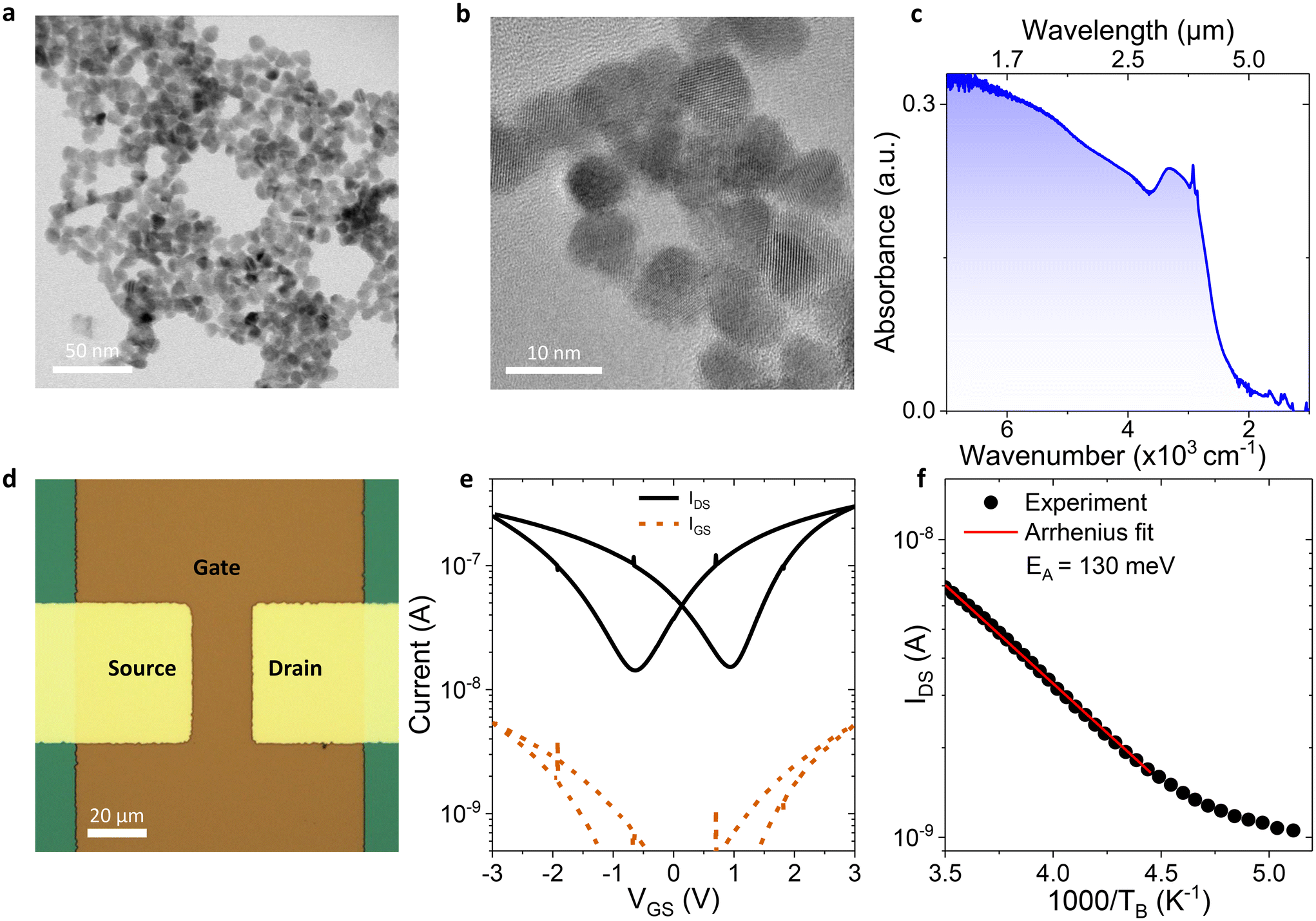 | ||
| Fig. 1 HgTe CQD-based field-effect transistor. (a) Transmission electron microscopy image of HgTe CQDs under study. (b) High-resolution TEM image of the same CQDs. (c) Absorption spectrum of the HgTe CQDs, after their liquid phase ligand exchange. The electronic transition overlaps with the narrow peak at 2900 cm−1 coming from the C–H bond. (d) Optical microscopy image of the FET with drain, source and gate electrodes. (e) Transfer curve (i.e., drain and gate current as a function of gate–source bias under constant drain–source bias, here 100 mV) for the FET whose channel is made of HgTe CQDs. (f) Current as a function of temperature under constant drain–source bias (100 mV) and its Arrhenius fit leading to an activation energy of 130 meV. | ||
Using conventional lithography procedures, we then design a field-effect transistor (see the procedure in Fig. S1†). A bottom gold electrode is separated from the channel by a 40 nm thick alumina layer. The drain and source electrodes are patterned on top of the gate dielectric (see Fig. 1d) and the whole system is then coated with the CQDs. The native capping ligands are replaced in solution using a hybrid surface chemistry combining ions (HgCl2) and short thiols (mercaptoethanol), as proposed previously.37,41 The I–V curve (Fig. S2†) is linear at room temperature, indicating the formation of ohmic contacts, thanks to the narrow band gap nature of the material, which minimizes any possible offset between the band energy and the electrodes’ work function. Upon gate bias application, a clear modulation of the drain–source current is observed (see Fig. 1e), with a signal significantly larger than the leakage current. The transfer curve (Fig. 1e) exhibits conduction under both negative bias (i.e., hole accumulation) and positive gate bias (i.e., electron accumulation), which is the expected behavior for an ambipolar material. Near room temperature (250 K), the gate-induced modulation of the current is limited to about one order of magnitude. This results from the large thermal activation of carriers in this material, limiting the reduction in the off-current (i.e., the current at the minimum of conduction). Higher current modulation can be obtained by further reducing the operating temperature,42 as pointed out by the I–T curve in Fig. 1f.
To probe the impact of a defective gate, we add a controlled etching step of the dielectric layer prior to deposition of the CQDs. Using e-beam lithography, we pattern the resist to selectively etch a square area with 3 μm edges on the gate dielectric. Such a defect mimics, in a controlled way, what can be induced, for example, by a metallic tweezer scratching the surface of a thin dielectric. The defect size is chosen to be small compared to the channel width (20 μm), ensuring that it remains a localized defect, yet large enough compared to the resolution of our photoemission imaging setup (approximately 700 nm) to clearly localize the gate hole (see the schematic of the device in Fig. 2b and S1†).
 | ||
| Fig. 2 Impact of defect on FET energy landscape. (a) Survey spectrum focused on the low binding energy region of the spectrum for an HgTe CQD film, acquired with 95 eV photon energy, highlighting the presence of Hg 5d and Te 4d states (see also Fig. S3†). (b) Schematic of the soft X-ray photoemission setup. The synchrotron beam is focused through a Fresnel zone plate (ZP) and an order selection aperture (OSA), reaching the sample with a 700 nm spot. For each position in the x–y plane, a photoemission spectrum is acquired by analyzing the kinetic energy of the emitted electrons using an electron energy analyzer. (c) Hg 5d5/2 binding energy map of the FET channel near the hole. The dashed lines are used to indicate the electrode localization. The localization of the hole is marked with a dashed square. (d) Hg 5d5/2 binding energy profile across the channel along a line intersecting the hole (at y = 0 μm) for various applied gate biases, under a −1 V drain–source bias. (e) Hg 5d5/2 binding energy profile across the channel along a line away from the hole (at y = 10 μm) for various applied gate biases, under a −1 V drain–source bias. (f) Energy shift value at x = 0 μm from the profiles shown in (d) (intersecting the hole, blue line) and (e) (away from the hole, black line) as a function of the applied gate bias. | ||
To map the energy landscape of the device in operando, we use a focused soft X-ray setup.43 The high flux from a synchrotron beam is focused using a Fresnel zone plate. The latter is optimized to operate at 95 eV, hence maximizing the available flux while offering the smallest spot size at the sample scale (700 nm). The sample is then mounted on a stage allowing for the application of bias, then scanned under the beam. For each position, a photoemission spectrum is collected, as depicted in Fig. 2b. HgTe presents the benefit of having two low-energy core levels that can be excited with the soft X-rays: Hg 5d with a binding energy of 8 eV (Hg 5d5/2) and Te 4d with a binding energy of 40 eV (Te 4d5/2)34 (see Fig. 2a and S3†).
Energy conservation44 (eqn (1)) is used to retrieve the binding energy (BE) from the kinetic energy (KE) measured using an analyzer through the equation:
| hv = BE(x,y,VDS,VGS) + KE(x,y,VDS,VGS) + WFA | (1) |
To unveil the energy landscape, we fit the acquired spectrum from each point with a Gaussian line shape and extract the peak energy of the tracked core level (see Fig. S4†). The obtained map actually mimics the expected shift of the valence band, if we assume a rigid shift of the whole XPS spectrum upon bias application. Even though the high conductivity of the sample (see Fig. 1e) already limits photo-charging effects, we further subtract the map obtained with all electrodes grounded from those taken under bias to obtain the energy shift map:
 | (2) |
This procedure eliminates possible residual photo-charging effects in the sample. Fig. S4† shows a complete description of the data processing. It is worth pointing out that, until the breakdown, the spectra relative to a core level are mostly shifted (i.e., neither broadening nor new components are observed) by bias application, as illustrated in Fig. S5.†
A typical map of the channel area around the defect is given in Fig. 2c, obtained here under a −1 V drain–source bias and a −3 V gate bias. The left and right sides of the map show homogeneous potentials, which is the expected behavior for the material atop the gold electrodes that set the potential. The potentials at the two electrodes are shifted by 1 eV, in agreement with the −1 V bias applied across the channel. Between the two electrodes, a potential gradient is observed, with the profile (black line in Fig. 2e) showing a continuous decrease of potential along the channel, without any accumulation of potential drop at the electrode interface (i.e., no Schottky barrier). This observation is consistent with the ohmic I-V curve observed from transport measurements (Fig. S2†). The defect from the gate is also clearly visible on this map, indicated by the blue feature at the bottom part of the map.
To quantify the impact of such a defective gate, we have tracked the potential along the channel for various gate biases, along a profile that overlaps with the gate hole (Fig. 2d, at y = 0 μm on Fig. 2c) and along a profile away from the hole (Fig. 2e, at y = 10 μm on Fig. 2c). Away from the defect (Fig. 2e), we observe a gate-induced shift towards lower binding energy under negative gate bias, which translates into a reduction of the energy difference between the valence band edge and the Fermi level, corresponding to a reinforced p-type behavior. Conversely, a positive gate bias leads to the opposite behavior. One can quantize the gate lever arm (the ability of the gate to shift the energy profile) by plotting the induced energy shift as a function of applied gate bias (Fig. 2f): a value of 0.25 eV.V−1 is obtained around the center of the channel.
Over the gate defect, the energy profile is significantly modified, as shown in Fig. 2d. The energy profile modulation is more intense and corresponds to a 1 eV.V−1 slope, as expected for a non-capacitive coupling (see Fig. 2f). To further understand how the defect disturbs the FET operation, we also examine the electric field distribution. Thanks to the high spatial resolution of the method, the electric field can be obtained from  , where V is the electric potential. Since we assume that the shifts in binding energy relative to the grounded configuration are solely due to the application of a bias, the electric field directly relates to the experimental data through
  , where ΔBE is the measured binding energy shift. In Fig. 3, we overlap the binding energy shift map with the electric field map, quantified by the direction and length of local arrows. These maps have been depicted for two cases. In Fig. 3a, a drain–source potential (−1 V) is applied while the gate is floating. In this case, the field is weak on both the left side and the right side of the image, corresponding to the area of the electrodes over which the potential is set by the underlying metal. It is worth noting that the presence of the defect does not prevent a bias application, as evidenced by the 1 eV difference in potential between electrodes. In the channel, the electric field is mostly homogeneous and directed toward the decreasing potential. In Fig. 3b, the potential of the gate is now set (VGS = −3 V). The energy map is dominated by the dielectric defect and the electric field lines form a point charge-like distribution around the defect, with arrows directed radially toward the center of the hole.
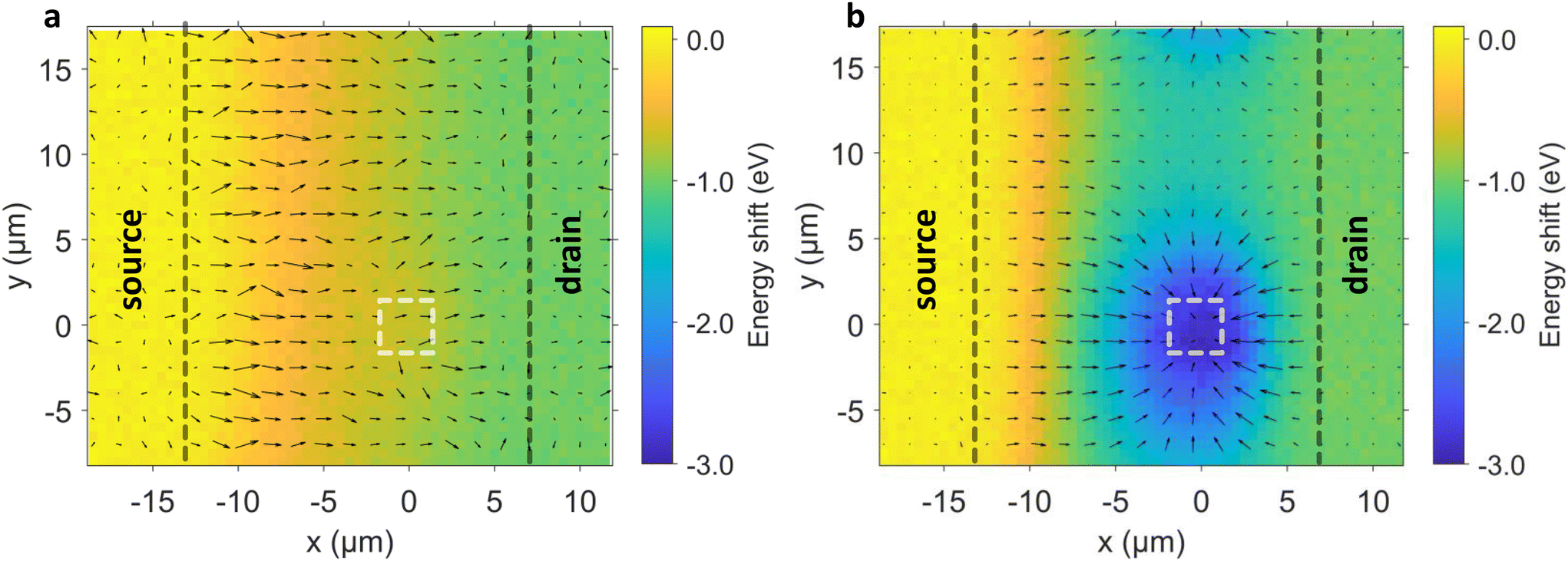 | ||
| Fig. 3 Mapping the current pathway. Energy shift map and vectorial distribution of the electric field, quantified through the direction and size of the arrows, for the floating gate (a) and VGS = −3 V (b), while a −1 V drain–source bias is applied. Dashed lines are used to indicate the electrode localization. | ||
Aside from the intensity of the modulation, the defect impacts spatially the whole channel (i.e., at a distance 5 times larger than the defect size). In other words, the gate defect generates a significant and long-distance modulation of the FET energy landscape. This long-range impact is particularly problematic for the operation of the FET, as it causes the entire energy profile to be dominated by a tiny defect, while the normal capacitive coupling of the rest of the gate appears as only a marginal modulation. This shows that even small degradations of the gate (a small percentage of the channel area) in the channel area can completely prevent the normal operation of the FET, although the effect is partly hidden from electrical output.
Though highly problematic, the local defect still allows for reversible FET operation (i.e., application of bias) and its impact can be minimized by keeping the gate floating, though this comes at the cost of losing the carrier density tunability. In the last part of the paper, we push further the degradation of the FET and operate the gate to induce irreversible damage. To reach such a breakdown, we apply an electric field of the order of 1 V nm−1 over the dielectric. Various degradation mechanisms have been observed depending on the channel thickness. The FET geometrical factors are also determinant in the actual breakdown mechanism. For the most resistive channel (see Fig. S7 and S8c†), corresponding to a thinner film coating (30 nm), the material within the channel is removed after the large gate bias application. This is likely due to film evaporation caused by the Joule effect. This process is difficult to investigate using photoemission imaging since there is no longer material available to track the potential. For this reason, we also prepared a sample with a slightly thicker channel (≈100 nm), and therefore a reduced resistance (see Fig. 4). Fig. 4a and b show optical images of the device, respectively, before and after the large gate bias application. In this case, the material within the channel is mostly preserved, enabling the tracking of the energy potential. Conversely, the interface between the drain–source electrode and the gate electrode presents a modified aspect. Energy dispersive X-ray spectroscopy (EDX, Fig. S5†) mapping shows the disappearance of Hg, Te and Al in this area, while one can notice an increased presence of silicon, which suggests that the substrate is now emerging from this area. We then analyze the FET operation in the channel after the high bias pulse (see Fig. 4c, d and S8b).† Though the energy profile is not exactly constant, the potential between the drain–source electrodes is no longer shifted by the amount of bias applied across the channel (−1 V). The potential is instead completely affected by the bias applied over the gate (+6 V), both for a line intersecting the hole (Fig. 4e) and for a line far away from the hole (Fig. 4f). Together with EDX mapping, these observations suggest that all electrodes are now shorted via the gate electrode.
 | ||
| Fig. 4 Breakdown of a FET. (a) (with respect to (b)) Optical microscopy image of the channel with two defects before (respectively, after) the application of a 40 V gate bias. (c) Zoomed-in view of the area corresponding to the dashed red rectangle from (b). (d) X-ray photoemission imaging relative to the Te 4d5/2 state around the same area as that shown in (c); the measurement was conducted after the high gate bias pulses, with VDS = −1 V and VGS = +6 V. (e) Energy profile of the Te 4d doublet over the defect (bottom yellow dashed line from (c) and (d) at y = 0 μm) from the map shown in (d). (f) The energy profile of the Te 4d doublet over the hole defect (top yellow dashed line from (c) and (d) at y = 10 μm) from the map shown in (d). | ||
Our study suggests a few strategies to limit defect formation and breakdown generation. First, defects within the thin dielectric can easily form through scratching. Therefore, FET handling should be conducted with appropriate tweezers, which must be kept far away from the active area. Secondly, the region where the drain–source electrodes overlap with the gate electrode clearly appears as one of the most fragile regions, and this area should be kept as small as possible. However, reducing the gate area to only a portion of the channel will lead to uneven doping.34 Thus, the gate electrode should just match the channel area. Additionally, it is probably critical to avoid large height discontinuities in this region, as this is more likely to generate pinholes in the dielectric. To address this, we recommend smooth edges for the bottom gate fabrication (e.g., using rotation during metal deposition) and conformal methods (such as ALD) for the dielectric deposition.
Conclusion
To conclude, we have demonstrated that XPS imaging appears highly suited to reveal the energy landscape of nanocrystal-based devices. Here, we specifically used the high resolution of the method as a way to reveal how a defective structure can impact the potential landscape. In particular, we bring evidence that even a very localized defect in the gate dielectric can impact the operability of the whole device. The defective gate induces a stronger and longer-distance (>10 μm) modulation of the channel profile than the nominal effect expected from the capacitive gate. This study highlights a critical weakness of FET analysis only based on electrical measurements, since local defects of the gate maintain device operability, though clearly not operating in its nominal manner. Additionally, XPS imaging appears suited to unveil how operations beyond the breakdown voltage contribute to irreversible changes in the operation of the device. This work stresses the importance of systematically combining electrical measurements with careful structural and local analysis in order to accurately assess the electrical operation of such devices. The generality of XPS imaging makes it particularly effective for directly identifying phenomena that might otherwise only be intuited from electrical measurements (such as ion migration and the presence of redox processes).Methods
Chemicals
Mercury chloride (HgCl2, Strem Chemicals, 99%), tellurium powder (Te, Sigma-Aldrich, 99.99%), trioctylphosphine (TOP, Alfa Aesar, 90%), oleylamine (Thermo Scientific, 80–90%), dodecanethiol (DDT, Sigma-Aldrich, 98%), 2-mercaptoethanol (MPOH, Thermo Scientific, 98%), N,N-dimethylformamide (DMF, VWR Rectapur), ethanol absolute anhydrous (EtOH, VWR), methanol (MeOH, VWR, Normapur), chloroform (VWR Technical), and chlorobenzene (VWR Rectapur) were used in this study. All chemicals are used as received, except oleylamine which is centrifuged before use. Mercury salts are toxic and must be handled with great care.![[thin space (1/6-em)]](https://www.rsc.org/images/entities/b_char_2009.gif) :Te precursor.
In a three-necked flask, 6.35 g of Te powder was mixed in 50 mL of TOP. The flask was kept under vacuum at room temperature for 5 minutes and then heated up to 100 °C and kept under vacuum for an additional 45 minutes. The atmosphere was changed to Ar and the temperature was raised to 275 °C. The solution was stirred until a clear orange color was obtained. The flask was then cooled down and the color switched to yellow. The flask was degassed again for 10 minutes at room temperature. Finally, this solution was transferred to a nitrogen-filled glovebox for storage.
:Te precursor.
In a three-necked flask, 6.35 g of Te powder was mixed in 50 mL of TOP. The flask was kept under vacuum at room temperature for 5 minutes and then heated up to 100 °C and kept under vacuum for an additional 45 minutes. The atmosphere was changed to Ar and the temperature was raised to 275 °C. The solution was stirred until a clear orange color was obtained. The flask was then cooled down and the color switched to yellow. The flask was degassed again for 10 minutes at room temperature. Finally, this solution was transferred to a nitrogen-filled glovebox for storage.
![[thin space (1/6-em)]](https://www.rsc.org/images/entities/char_2009.gif) :Te (1 M) and 8 mL of oleylamine was quickly injected. After 3 minutes, 10 mL of a mixture of 10% vol. of DDT in toluene was injected and a water bath was used to rapidly decrease the temperature. The content of the flask was split over three centrifuge tubes. The solution was precipitated first with MeOH and the resulting pellet was redispersed in one centrifuge tube with chloroform. A second precipitation was completed with absolute EtOH, and the formed pellet was redispersed in 6 mL of chlorobenzene.
:Te (1 M) and 8 mL of oleylamine was quickly injected. After 3 minutes, 10 mL of a mixture of 10% vol. of DDT in toluene was injected and a water bath was used to rapidly decrease the temperature. The content of the flask was split over three centrifuge tubes. The solution was precipitated first with MeOH and the resulting pellet was redispersed in one centrifuge tube with chloroform. A second precipitation was completed with absolute EtOH, and the formed pellet was redispersed in 6 mL of chlorobenzene.
Transmission electron microscopy
A drop of diluted solution of CQDs was cast on a copper grid covered with an amorphous carbon film. The grid was degassed overnight under a secondary vacuum. A JEOL 2010F instrument was used at 200 kV for the acquisition of pictures.Infrared spectroscopy
A Fischer Nicolet iS50 in attenuated total reflection (ATR) mode was used. The spectra were averaged over 32 acquisitions and have a 4 cm−1 resolution.Photoemission microscopy
Photoemission microscopy was conducted at the ANTARES beamline of Synchrotron SOLEIL. The synchrotron beam, which is ≈2.5–3 mm wide, was focused using a zone plate (i.e., Fresnel lens) (see Fig. 2b). The latter was operated at low energy (below 100 eV) to achieve optimal focusing. In this case, the beam width at the sample position can be focused to around 700 nm. The sample was then scanned and the photoelectrons were collected using an MBS A-1 hemispherical electron analyzer.43 The sample holder was moved with step sizes ranging from 500 to 2000 nm and, for each point, a series of photoemission spectra were collected. These spectra were acquired with a 200 eV pass energy, providing a 15.8 eV window with a 17 meV energy step, and were then averaged. Here, we focused on the Hg 5d doublet, with a spin–orbit (SO) splitting of 1.8 eV and a binding energy for the Hg 5d5/2 of around 8 eV, and on the Te 4d doublet with an SO splitting of 1.44 eV and a binding energy for the Te 4d5/2 of around 40 eV (see Fig. S3).† Data acquisition lasted from a few minutes to an hour, depending on the targeted map size. For acquisition with bias applied, we systematically subtracted the grounded map during data analysis to remove possible photocharging effects. We used linearly horizontal polarized photons with a photon energy of 95 eV and all measurements were conducted at 250 K, with the combined energy resolution better than 120 meV. For all maps, the angular dispersion of the analyzer (±15°) was neglected by integrating the spectra over all angles. The samples were mounted on the operando sample holder of the ANTARES beamline, which was equipped with electrical contacts. These electrical contacts were made through gold wires which were bonded to the electrical pads of the sample holder, while silver paste was applied to the electrical pads of the sample. The sample was connected to two Keithley 2450 units to apply drain and gate biases.Electrode fabrication
The substrate (Si/SiO2 wafer, 300 nm oxide layer) was cleaned by sonication in an acetone bath and then rinsed with acetone and IPA and dried with an N2 gun. Final cleaning was achieved using O2 plasma. First, the gates were patterned by photolithography. An adhesion primer (TI PRIME) was spin-coated and then baked at 110 °C for 1 minute. Then, the photoresist (AZ5214E) was spin-coated and baked at 110 °C for 1 minute before UV exposure of 1.5 seconds through the lithography mask. The sample was then baked at 110 °C for 2 minutes for resist inversion, and flood exposed to UV light for 40 seconds. Development was carried out for 20 seconds in AZ 726MIF, followed by rinsing in de-ionized water. The sample was plasma cleaned before thermal evaporation of the metal for the electrodes (5 nm Cr/40 nm Au). Lift-off was carried out in an acetone bath for 30 minutes. After fabrication of the gate electrodes, 40 nm of Al2O3 was deposited by atomic layer deposition (ALD, 450 cycles) to form the gate dielectric. Finally, a second photolithographic process was performed to pattern the source and drain electrodes, with evaporation of 5 nm Ti/40 nm Au.Defect fabrication
The defects in the alumina were introduced to the previously prepared electrodes through electron beam lithography. The substrates were rinsed with acetone and IPA. Undiluted PMMA was spin-coated at 4000 rpm for 30 seconds (1000 rpm s−1 acceleration) to obtain a thick PMMA layer (∼500 nm). The PMMA layer was then baked at 175 °C for 3 minutes. 10 nm of Al was deposited by thermal evaporation right before transfer to the SEM chamber. E-beam lithography was performed at 200 μC cm−2 exposure. The pattern consists of 2 square holes, 3 μm wide and 20 μm apart, centered in the middle of the channel. The Al layer was then removed with a dilute (<4%) KOH bath and rinsed with water. The pattern was developed with an MIBK/IPA solution (1:3) for 60 seconds and rinsed with IPA. The alumina was etched with an AZ 726 MIF developer heated at 60 °C for 2 minutes and rinsed with water. Lift-off of the PMMA was performed in acetone overnight.
HgTe CQDs film deposition
A ligand exchange solution was prepared with 15 mg of HgCl2 dissolved in 9 mL of DMF, to which 1 mL of MPOH was added. 500 μL of CQD solution (with a concentration of 50 mg mL−1 in chlorobenzene) was mixed with 500 μL of the ligand exchange solution and 5 mL of hexane. Then, 500 μL of DMF was added and the mixture was sonicated and mixed. The CQDs underwent a phase transfer from the apolar phase to the DMF phase. The clear apolar phase was discarded using a pipette and two additional rounds of cleaning with hexane were performed. Once the apolar phase was removed, the CQDs were precipitated by adding a few drops of toluene and centrifuging at 6000 rpm for 3 minutes. A pellet formed, which was then redispersed in 200 μL of DMF. To obtain a film of 90–100 nm thickness, 8 μL of the ink solution was spin-coated on the sample at 4000 rpm for 45 seconds. For a 30 nm film, the ink solution was diluted twice with DMF, and 8 μL was then spin-coated at 4000 rpm for 45 seconds.Author contributions
EL and DP designed and supervised the project and obtained funding. YP grew the nanocrystals. MC built devices with the assistance of ED. CG, TG, AC, AK and SI conducted some material characterization studies. MC, DM and EB acquired photoemission data under the guidance of PD and JA. MC and EL wrote the manuscript, which has been proofread by all authors.Data availability
The data that support the findings of this study are available from the corresponding author upon request.Conflicts of interest
The authors declare no competing interests.Acknowledgements
We thank Stephane Lorcy for his help in sample preparation. The project was supported by ERC grant AQDtive (grant no. 101086358) and the French National Research Agency (ANR) through the grants Bright (ANR-21-CE24-0012-02), MixDferro (ANR-21-CE09-0029), Quicktera (ANR-22-CE09-0018), Operatwist (ANR-22-CE09-0037-01), E-map (ANR-23-CE50-0025), DIRAC (ANR-24-ASM1-0001), camIR (ANR-24-CE42-2757), and Piquant (ANR-24-CE09-0786) and as part of the “Investissements d'Avenir” program (LabEx NanoSaclay, reference: ANR-10-LABX-0035). We acknowledge the use of clean-room facilities from the “Centrale de Proximité Paris-Centre” and support from Renatech+ for micro and nanofabrication. This project has also received financial support from the CNRS through the MITI interdisciplinary programs (project WITHIN) and Region Ile de France through the Sesame project INSIDE.References
- M. Liu, N. Yazdani, M. Yarema, M. Jansen, V. Wood and E. H. Sargent, Nat. Electron., 2021, 4, 548–558 CrossRef.
- J. Kim, J. Roh, M. Park and C. Lee, Adv. Mater., 2024, 36, 2212220 CrossRef CAS PubMed.
- Y. Shu, X. Lin, H. Qin, Z. Hu, Y. Jin and X. Peng, Angew. Chem., 2020, 132, 22496–22507 CrossRef.
- J. Liu, P. Liu, D. Chen, T. Shi, X. Qu, L. Chen, T. Wu, J. Ke, K. Xiong, M. Li, H. Song, W. Wei, J. Cao, J. Zhang, L. Gao and J. Tang, Nat. Electron., 2022, 5, 443–451 CrossRef.
- C. Gréboval, D. Darson, V. Parahyba, R. Alchaar, C. Abadie, V. Noguier, S. Ferré, E. Izquierdo, A. Khalili, Y. Prado, P. Potet and E. Lhuillier, Nanoscale, 2022, 14, 9359–9368 RSC.
- G. Mu, Y. Tan, C. Bi, Y. Liu, Q. Hao and X. Tang, Nat. Photonics, 2024, 18, 1147–1154 CrossRef CAS.
- D. V. Talapin and C. B. Murray, Science, 2005, 310, 86–89 CrossRef CAS PubMed.
- D. V. Talapin, J.-S. Lee, M. V. Kovalenko and E. V. Shevchenko, Chem. Rev., 2010, 110, 389–458 CrossRef CAS PubMed.
- F. Hetsch, N. Zhao, S. V. Kershaw and A. L. Rogach, Mater. Today, 2013, 16, 312–325 CrossRef CAS.
- Y. Liu, M. Gibbs, J. Puthussery, S. Gaik, R. Ihly, H. W. Hillhouse and M. Law, Nano Lett., 2010, 10, 1960–1969 CrossRef CAS PubMed.
- M. Chen, H. Lu, N. M. Abdelazim, Y. Zhu, Z. Wang, W. Ren, S. V. Kershaw, A. L. Rogach and N. Zhao, ACS Nano, 2017, 11, 5614–5622 CrossRef CAS PubMed.
- M. Cavallo, E. Bossavit, H. Zhang, C. Dabard, T. H. Dang, A. Khalili, C. Abadie, R. Alchaar, D. Mastrippolito, Y. Prado, L. Becerra, M. Rosticher, M. G. Silly, J. K. Utterback, S. Ithurria, J. Avila, D. Pierucci and E. Lhuillier, Nano Lett., 2023, 23, 1363–1370 CrossRef CAS PubMed.
- S.-S. Chee, C. Gréboval, D. V. Magalhaes, J. Ramade, A. Chu, J. Qu, P. Rastogi, A. Khalili, T. H. Dang, C. Dabard, Y. Prado, G. Patriarche, J. Chaste, M. Rosticher, S. Bals, C. Delerue and E. Lhuillier, Nano Lett., 2021, 21, 4145–4151 CrossRef CAS PubMed.
- A. G. Shulga, S. Kahmann, D. N. Dirin, A. Graf, J. Zaumseil, M. V. Kovalenko and M. A. Loi, ACS Nano, 2018, 12, 12805–12813 CrossRef CAS PubMed.
- U. N. Noumbé, C. Gréboval, C. Livache, A. Chu, H. Majjad, L. E. Parra López, L. D. N. Mouafo, B. Doudin, S. Berciaud, J. Chaste, A. Ouerghi, E. Lhuillier and J.-F. Dayen, ACS Nano, 2020, 14, 4567–4576 CrossRef PubMed.
- A. Nag, M. V. Kovalenko, J.-S. Lee, W. Liu, B. Spokoyny and D. V. Talapin, J. Am. Chem. Soc., 2011, 133, 10612–10620 CrossRef CAS PubMed.
- M. V. Kovalenko, M. Scheele and D. V. Talapin, Science, 2009, 324, 1417–1420 CrossRef CAS PubMed.
- A. T. Fafarman, W. Koh, B. T. Diroll, D. K. Kim, D.-K. Ko, S. J. Oh, X. Ye, V. Doan-Nguyen, M. R. Crump, D. C. Reifsnyder, C. B. Murray and C. R. Kagan, J. Am. Chem. Soc., 2011, 133, 15753–15761 CrossRef CAS.
- J.-H. Choi, H. Wang, S. J. Oh, T. Paik, P. Sung, J. Sung, X. Ye, T. Zhao, B. T. Diroll, C. B. Murray and C. R. Kagan, Science, 2016, 352, 205–208 CrossRef CAS PubMed.
- D. K. Kim, Y. Lai, B. T. Diroll, C. B. Murray and C. R. Kagan, Nat. Commun., 2012, 3, 1216 CrossRef PubMed.
- T. P. Osedach, N. Zhao, T. L. Andrew, P. R. Brown, D. D. Wanger, D. B. Strasfeld, L.-Y. Chang, M. G. Bawendi and V. Bulović, ACS Nano, 2012, 6, 3121–3127 CrossRef CAS PubMed.
- J. Tolentino, M. Gibbs, A. Abelson and M. Law, J. Chem. Phys., 2023, 159, 044709 CrossRef CAS PubMed.
- S. Tanwar, R. Millan-Solsona, S. Ruiz-Molina, M. Mas-Torrent, A. Kyndiah and G. Gomila, Adv. Mater., 2024, 36, 2309767 CrossRef CAS PubMed.
- Y. Zhang, D. Zherebetskyy, N. D. Bronstein, S. Barja, L. Lichtenstein, D. Schuppisser, L.-W. Wang, A. P. Alivisatos and M. Salmeron, Nano Lett., 2015, 15, 3249–3253 CrossRef CAS PubMed.
- Y. Zhang, D. J. Hellebusch, N. D. Bronstein, C. Ko, D. F. Ogletree, M. Salmeron and A. P. Alivisatos, Nat. Commun., 2016, 7, 11924 CrossRef CAS PubMed.
- P. Majchrzak, R. Muzzio, A. J. H. Jones, D. Curcio, K. Volckaert, D. Biswas, J. Gobbo, S. Singh, J. T. Robinson, K. Watanabe, T. Taniguchi, T. K. Kim, C. Cacho, J. A. Miwa, P. Hofmann, J. Katoch and S. Ulstrup, Small Sci., 2021, 1, 2000075 CrossRef CAS.
- P. Hofmann, AVS Quantum Sci., 2021, 3, 021101 CrossRef CAS.
- Y.-Y. Lu, Y.-L. Yang, P.-Y. Chuang, J. Jhou, J.-H. Hsu, S.-H. Hsieh and C.-H. Chen, Nanotechnology, 2022, 33, 475702 CrossRef CAS PubMed.
- J. Avila, I. Razado-Colambo, S. Lorcy, B. Lagarde, J.-L. Giorgetta, F. Polack and M. C. Asensio, J. Phys.: Conf. Ser., 2013, 425, 192023 CrossRef.
- M. Cavallo, E. Bossavit, S. Matzen, T. Maroutian, R. Alchaar, T. H. Dang, A. Khalili, C. Dabard, H. Zhang, Y. Prado, C. Abadie, J. K. Utterback, J. F. Dayen, M. G. Silly, P. Dudin, J. Avila, E. Lhuillier and D. Pierucci, Adv. Funct. Mater., 2023, 33, 2300846 CrossRef CAS.
- M. Cavallo, A. Ram, S. Pandey, T. Maroutian, E. Bossavit, N. Ledos, A. Khalili, H. Zhang, Y. Prado, D. L. Nguyen, T. H. Dang, H. Majjad, J. Biscaras, J. Avila, J. F. Dayen, E. Lhuillier and D. Pierucci, Appl. Phys. Lett., 2023, 123, 253505 CrossRef CAS.
- M. Cavallo, R. Alchaar, E. Bossavit, H. Zhang, T. H. Dang, A. Khalili, Y. Prado, M. G. Silly, J. K. Utterback, S. Ithurria, P. Dudin, J. Avila, D. Pierucci and E. Lhuillier, Nanoscale, 2023, 15, 9440–9448 RSC.
- A. Khalili, M. Cavallo, E. Bossavit, R. Alchaar, T. H. Dang, C. Dabard, H. Zhang, N. Ledos, V. Parahyba, P. Potet, J. K. Utterback, Y. Prado, M. G. Silly, P. Dudin, J. Avila, D. Pierucci and E. Lhuillier, ACS Appl. Electron. Mater., 2023, 5, 4377–4384 CrossRef CAS.
- M. Cavallo, D. Mastrippolito, E. Bossavit, L. Curti, A. Khalili, H. Zhang, N. Ledos, Y. Prado, E. Dandeu, M. Rosticher, S. Ithurria, P. Dudin, J. Avila, D. Pierucci and E. Lhuillier, Nano Res., 2024, 17, 10376–10385 CrossRef CAS.
- C. Gréboval, A. Chu, N. Goubet, C. Livache, S. Ithurria and E. Lhuillier, Chem. Rev., 2021, 121, 3627–3700 CrossRef PubMed.
- K. A. Sergeeva, H. Zhang, A. S. Portniagin, E. Bossavit, G. Mu, S. V. Kershaw, S. Ithurria, P. Guyot-Sionnest, S. Keuleyan, C. Delerue, X. Tang, A. L. Rogach and E. Lhuillier, Adv. Funct. Mater., 2024, 34, 2405307 CrossRef CAS.
- X. Lan, M. Chen, M. H. Hudson, V. Kamysbayev, Y. Wang, P. Guyot-Sionnest and D. V. Talapin, Nat. Mater., 2020, 19, 323–329 CrossRef CAS PubMed.
- J. Qu, M. Weis, E. Izquierdo, S. G. Mizrahi, A. Chu, C. Dabard, C. Gréboval, E. Bossavit, Y. Prado, E. Péronne, S. Ithurria, G. Patriarche, M. G. Silly, G. Vincent, D. Boschetto and E. Lhuillier, Nat. Photonics, 2022, 16, 38–44 CrossRef CAS.
- S. Keuleyan, E. Lhuillier and P. Guyot-Sionnest, J. Am. Chem. Soc., 2011, 133, 16422–16424 CrossRef CAS PubMed.
- A. Rogach, S. V. Kershaw, M. Burt, M. T. Harrison, A. Kornowski, A. Eychmüller and H. Weller, Adv. Mater., 1999, 11, 552–555 CrossRef CAS.
- B. Martinez, J. Ramade, C. Livache, N. Goubet, A. Chu, C. Gréboval, J. Qu, W. L. Watkins, L. Becerra, E. Dandeu, J. L. Fave, C. Méthivier, E. Lacaze and E. Lhuillier, Adv. Opt. Mater., 2019, 7, 1900348 CrossRef.
- E. Lhuillier, S. Keuleyan, P. Zolotavin and P. Guyot-Sionnest, Adv. Mater., 2013, 25, 137–141 CrossRef CAS.
- J. Avila, S. Lorcy and P. Dudin, J. Electron Spectrosc. Relat. Phenom., 2023, 266, 147362 CrossRef CAS.
- W. F. Egelhoff, Surf. Sci. Rep., 1987, 6, 253–415 CrossRef.
Footnote |
| † Electronic supplementary information (ESI) available: (i) Procedure for the fabrication of the FET, (ii) XPS spectra from Hg 5d and Te 4d states, (iii) procedure to process the XPS imaging map and (iv) structural characterization of the FET after exposure to gate breakdown bias. See DOI: https://doi.org/10.1039/d5nr00767d |
| This journal is © The Royal Society of Chemistry 2025 |