
 Open Access Article
 This Open Access Article is licensed under a Creative Commons Attribution-Non Commercial 3.0 Unported Licence
An ultra-high-speed vertically illuminated self-driven lateral asymmetric InSe photodetector†
Srinivasa Reddy
Tamalampudi‡
 *,
Ghada
Dushaq‡
and
Mahmoud S.
Rasras
*
*,
Ghada
Dushaq‡
and
Mahmoud S.
Rasras
*
Department of Electrical Engineering, New York University Abu Dhabi, United Arab Emirates. E-mail: st4212@nyu.edu; mr5098@nyu.edu
First published on 23rd May 2025
Abstract
Two-dimensional (2D) materials have emerged as a promising platform for next-generation optoelectronic devices due to their unique electronic, optical, and mechanical properties, offering unprecedented opportunities for high-performance, low-power photodetection. We demonstrate a high-speed, zero-bias Au–InSe–multilayered graphene photodetector with an ultra-low dark current of 0.1 nA and photovoltaic-effect-driven photocurrent generation. The device exhibits a responsivity of 57.15 mA W−1 and a detectivity of 1.58 × 10⁹ Jones at a wavelength of 785 nm. The device achieves an RF 3 dB bandwidth of 2.5 MHz, corresponding to an ultrafast response time of 140 ns, establishing a new benchmark for zero-bias InSe photodetectors. The exceptional performance is attributed to using asymmetric electrodes, which establish a built-in electric field within the depletion region. This field facilitates the rapid separation of photogenerated electron–hole pairs, which reduces carrier lifetime and minimizes recombination effects, thereby significantly boosting the response speed. Our results underscore the potential of InSe photodetectors with asymmetric contacts for achieving low dark current, high-speed operation, and low power consumption, offering a promising pathway for the development of next-generation optoelectronic devices based on 2D materials.
Introduction
Photodetectors are indispensable in various applications, including environmental monitoring, optical imaging, communication systems, and surveillance.1,2 Recently, photodetection based on van der Waals multilayered two-dimensional (2D) materials has attracted significant attention due to their unique characteristics, such as a layer-dependent bandgap and exceptional optical absorption. These properties have opened new avenues for innovation in photodetection technologies. Key metrics for evaluating photodetector performance are response time and photoresponsivity. The response time defines a device's ability to track fast signals, while photoresponsivity quantifies its sensitivity to incident illumination.Despite their promising characteristics, most photodetectors based on 2D semiconductors suffer from slow response times, typically in the millisecond-to-microsecond range. This limitation arises from long carrier lifetimes, low mobility, and suboptimal device architectures.3–5 Overcoming these challenges is vital to unlocking the full potential of 2D semiconductor-based photodetectors in advanced applications. Therefore, it is imperative to explore strategies that can reduce response times without compromising photoresponsivity.
Among the various types of photodetectors, photovoltaic devices, such as self-powered photodetectors based on p–n junctions and Schottky diodes, have shown potential for significantly higher frequency responses compared to photoconductive detectors. Their architecture reduces carrier transit time by utilizing built-in electric fields to efficiently separate photogenerated charge carriers. Furthermore, the absence of a requirement for an external power source for photocurrent generation enhances their overall performance. Self-powered photodetectors based on 2D semiconductor materials often rely on heterojunctions with other 2D materials (e.g., graphene/InSe/MoS2 and InSe/SnS2), chemical doping, split-gate tuning, geometrically asymmetric contact areas, photothermoelectric (PTE) devices, and engineered electrode designs in Schottky junctions to suppress interface doping.6–8 While these strategies have achieved high responsivities, the response times of such devices remain suboptimal, limiting their suitability for high-speed applications.6
Previous research on 2D indium selenide (InSe) has demonstrated its exceptional optical properties, including high absorption, a direct bandgap, and tunable characteristics across visible to near-infrared (NIR) wavelengths.9 Notably, InSe-based photodetectors have achieved remarkable responsivities, reaching up to ∼105 A W−1, showcasing their potential for highly sensitive photodetection.10,11 Advances in device engineering, such as incorporating graphene electrodes to reduce contact resistance or utilizing h-BN encapsulation to minimize environmental degradation and preserve intrinsic material properties, have further enhanced the performance of these photodetectors.10,12 Additionally, vertically illuminated self-powered photodetectors based on 2D InSe have been investigated utilizing its inherent built-in electric fields to achieve efficient charge separation.13,14 Various approaches have been employed to enhance their performance, including the use of asymmetric contact area geometries with symmetric planar metal architectures, asymmetric metal contacts, and van der Waals junctions formed with other 2D materials such as graphene and transition metal dichalcogenides (TMDs).6,14 However, despite these advancements, the response speed of InSe self-driven detectors remains constrained within the millisecond-to-microsecond range, highlighting a critical area for improvement in future research to enable high-speed applications.
In this work, we present a self-driven InSe photodetector based on a Schottky junction with an Au–InSe–multilayer Gr/Au configuration. Under 785 nm illumination, the device achieves a 3 dB bandwidth of 2.5 MHz and a response time of 140 ns, surpassing the performance of previously reported self-driven InSe photodetectors. These findings highlight the exceptional potential of InSe for developing high-speed, energy-efficient photodetectors, while also showcasing its compatibility for seamless integration into advanced photonic platforms, paving the way for next-generation optoelectronic technologies.
Results and discussion
Material characterization of multilayered 2D InSe
InSe single crystals were grown using the Bridgman method.9 The chemical composition, morphology, and crystalline phase of the grown crystal flakes were characterized using scanning electron microscopy (SEM) with energy-dispersive X-ray spectroscopy (EDS) and X-ray diffraction (XRD). The EDS scan of the bulk crystal, performed over an area of 100 μm2 (Fig. 1a), revealed peaks corresponding exclusively to indium (In) and selenium (Se). Elemental mapping confirmed a homogeneous distribution of In and Se with a stoichiometric ratio of approximately 1![[thin space (1/6-em)]](https://www.rsc.org/images/entities/char_2009.gif) :1. To verify the crystallographic structure and phase of InSe, XRD measurements were performed on the bulk crystal at room temperature (Fig. S1†). The diffraction peaks matched well with the β-phase of InSe, indexed to a hexagonal structure with lattice constants a = b = 4.005 Å and c = 16.64 Å (JCPDS-34-1431). A schematic representation of the hexagonal lattice structure, showing the close-packed monoatomic Se–In–In–Se sequence, is provided in Fig. 1b. β-InSe is the most stable InSe phase due to its ABAB stacking order (hexagonal structure). It exhibits a moderate bandgap value (2.4 eV for monolayer and 1.4 eV for few-layer structures), making it suitable for broadband optoelectronics. The valence band maximum (VBM) shifts with thickness, influencing band alignment and carrier mobility, which are key factors in optimizing device performance.
:1. To verify the crystallographic structure and phase of InSe, XRD measurements were performed on the bulk crystal at room temperature (Fig. S1†). The diffraction peaks matched well with the β-phase of InSe, indexed to a hexagonal structure with lattice constants a = b = 4.005 Å and c = 16.64 Å (JCPDS-34-1431). A schematic representation of the hexagonal lattice structure, showing the close-packed monoatomic Se–In–In–Se sequence, is provided in Fig. 1b. β-InSe is the most stable InSe phase due to its ABAB stacking order (hexagonal structure). It exhibits a moderate bandgap value (2.4 eV for monolayer and 1.4 eV for few-layer structures), making it suitable for broadband optoelectronics. The valence band maximum (VBM) shifts with thickness, influencing band alignment and carrier mobility, which are key factors in optimizing device performance.
 | ||
| Fig. 1 Material properties of InSe nanosheets. (a) elemental mapping obtained via energy-dispersive X-ray spectroscopy (EDS) over the area scanned in the SEM image of a bulk InSe crystal (inset), showing a homogeneous distribution of elements with the corresponding EDS spectrum and the calculated weight and atomic ratios of In and Se. (b) Schematic ball-and-stick representation of the hexagonal crystal structure of InSe. (c) Atomic force microscopy (AFM) scan of a multilayer InSe nanosheet, showing a thickness of ∼20 nm (approximately 25 InSe layers). (d) Raman spectra of InSe flakes at room temperature, highlighting vibrational modes A1g(1), E2g(1), and A1g(2), measured using 532 nm laser excitation. | ||
The thickness of the exfoliated multilayer InSe nanosheets was determined via AFM to range from ∼20 nm to ∼50 nm, corresponding to approximately 25–63 layers of InSe (Fig. 1c). The AFM analysis revealed a relatively smooth surface for the exfoliated InSe sheets, which is crucial for their integration into photonic and electronic applications.15,16 Raman spectroscopy was conducted to confirm the phonon vibrational modes of the exfoliated InSe nanosheets. As shown in Fig. 1d, three prominent peaks were observed at 116 cm−1, 179.1 cm−1 and 227.4 cm−1, corresponding to the A1g(1), E2g(1), and A1g(2) modes, respectively.9 These observations are consistent with previously reported vibrational modes of β-phase InSe, further corroborating the material's phase.9
Device architecture and electrical characteristics of the asymmetric Au–InSe–Gr lateral diode in the dark state
To realize an InSe Schottky diode, asymmetric contacts were designed using Au and graphene (Gr) based on their distinct energy band structures. This configuration leverages the work function difference between Au (5.1 eV) and graphene (∼4.7 eV) to create an asymmetric Schottky barrier.14 The planar architecture, configured as back-to-back diodes, ensures low capacitance. The diodes were prepared on a 300 nm SiO2/Si substrate. Cr/Au metal electrodes were patterned and pre-deposited onto the substrate, followed by the dry mechanical transfer of a multilayer graphene flake onto one electrode using a custom-aligned transfer system.15,16Subsequently, exfoliated InSe nanosheets were transferred, forming the asymmetric Au–InSe–Gr/Au configuration, as illustrated in Fig. 2a. It is important to note that the dry transfer process preserves the intrinsic properties of InSe more effectively than wet processing techniques, such as those involving photolithography.17 This advantage arises because the properties of 2D materials are predominantly governed by their surface characteristics, making them highly sensitive to environmental perturbations. The band diagram of the prepared device at thermal equilibrium (V = 0 V) is depicted in Fig. 2b. The Schottky barrier heights at the metal contacts are denoted as ϕ1 and ϕ2, respectively. The potential barrier height for electrons is determined using Φbh = Φm − χs, where Φm represents the metal work function and χs is the electron affinity of the semiconductor. In this case, the calculation utilizes the electron affinity of InSe, which is 4.05 eV. The depletion region widths are labeled as W1 and W2. This asymmetry in barrier heights induces a built-in electric field, effectively suppresses dark current noise and enables self-driven photodetection.14
 | ||
| Fig. 2 Device structure and electrical characteristics in the dark state. (a) 3D schematic representation of the InSe Schottky diode. (b) Band diagram of the asymmetric metal contacts of Au–InSe–Gr. (c) Characteristic I–V profile of the Au–InSe–Gr diode; the inset shows a schematic of the back-to-back diode. | ||
The dark current–voltage (Isd–Vds) characteristics of the planar Au–InSe–Gr device exhibit standard rectification behavior, as shown in Fig. 2c. The device demonstrates a low leakage current of approximately 0.1 nA at a reverse bias of 1 V, with a rectification ratio of ∼103 under an operating condition of 4 V. It is worth noting that the rectification ratio, induced by the asymmetrical contacts, is influenced by the energy barrier height. This performance can be further enhanced by replacing the Au metal contact with metals possessing higher work functions, such as Pd or Pt.18 Furthermore, we measured the Ids–Vds characteristics of the symmetric Al–InSe–Al device for comparison. The device exhibits semi-ohmic behavior under dark conditions (see Fig. S2†).
Electro-optic characterization
To investigate the photoresponse of the fabricated Au–InSe–Gr device, its electrical output characteristics (Isd–Vds) were measured under both dark and illuminated conditions. The optical image of the prepared device is shown in the inset of Fig. 3a. A 785 nm laser illuminated the device while Vds was swept between −3 V and 3 V. Measurements were conducted at various incident light intensities (P) ranging from 0.63 μW to 2.61 μW, as shown in Fig. 3(a). The device exhibited diode-like behavior under both dark and light conditions due to the depletion region formed by the asymmetric contacts. | ||
| Fig. 3 Optoelectronic characterization of an InSe photodetector with asymmetric contacts. (a) Characteristic output curves of the InSe photodetector measured in the dark and under 785 nm illumination at various excitation power values. The inset shows an optical image of the fabricated device, with a scale bar of 10 μm. The transferred graphene and InSe are highlighted by red and black dashed-line boxes, respectively. (b) Photocurrent as a function of incident laser power at Vds = 0 V. (c) Open-circuit voltage (Voc) and short-circuit current (Isc) as a function of incident power. (d) Measured responsivity and external quantum efficiency (EQE) values as a function of incident power intensity under Vds = 0 V at 785 nm excitation. | ||
The photocurrent (Iph = Ilight − Idark) was measured at 0 V as a function of incident laser power to examine the effect of the built-in electric field on photogenerated carriers (Fig. 3b). The photocurrent demonstrated a linear relationship with incident light power, following the power-law dependence Iph ∝ Pα, where α ≈ 0.91. This indicates efficient electron–hole pair separation and suggests that the photocurrent increases proportionally with light intensity.19
The primary mechanism responsible for photocurrent generation is the photovoltaic effect. The built-in electric field from the asymmetric contacts facilitates the efficient separation and collection of photogenerated carriers at the InSe/electrode interface. This mechanism, driven by a carrier concentration gradient, ensures rapid electron–hole pair separation and is characteristic of photovoltaic operation.20,21
Due to this photovoltaic mechanism, the photodetector operates without an external bias, exhibiting self-powered behavior. The photogenerated current was observed even at a bias of 0 V under illumination. Two critical parameters for evaluating self-powered capability are the short-circuit current (Isc) and open-circuit voltage (Voc). As shown in Fig. 3(c), both Voc and Isc increase with light power. The maximum Voc of 0.23 V corresponds to the barrier height difference between the two metal–semiconductor (MS) junctions. At low incident power, the relatively lower Voc is attributed to the reverse-bias of the dark current of the graphene–InSe junction, which offsets the photocurrent difference between the MS junctions. Generally, in photovoltaic systems, Voc tends to scale logarithmically or linearly with power, rather than following a power law. This is due to the dependence of Voc on the photogenerated carrier density. The linear relationship between Isc and light power demonstrates the device's potential for optical signal photodetection applications.
Photoresponsivity (R) is a key performance parameter for photodetectors and is expressed as R = Iph/P·S, where Iph is the photocurrent, P is the incident optical power density, and S is the detector area. The calculated R as a function of incident power is shown in Fig. 3(d). The maximum responsivity measured was 57.15 mA W−1 under 785 nm illumination at a laser power of 0.908 μW (Iph = 51.9 nA, P = 16.35 μW cm−2, S = 555.5 μm2, with a spot size radius of 250 μm) at Vds = 0 V. In photoconductive devices, responsivity typically decreases with increasing optical power due to trap saturation and minority carrier recombination. However, in the InSe device with asymmetric contacts, the responsivity remains constant across all incident optical power levels, which is similar to the reported self-bias response of the photodetectors.22 This behavior is attributed to the photovoltaic mechanism, which ensures a direct and linear relationship between absorbed photons and collected carriers without involving a gain mechanism or external carrier injection. Furthermore, the incident power levels used in this study are insufficient to induce nonlinear effects such as absorption saturation, carrier recombination, or heating, thereby maintaining stable device performance. Additionally, the calculated external quantum efficiency (EQE) also exhibits minimal dependence on the incident power, as shown in Fig. 3(d).
The speed response of the asymmetric Au–InSe–Gr photodetector
To characterize the dynamic performance of the photodetector, the normalized time/frequency responses were measured using the experimental setup shown schematically in Fig. 4(a). The InSe device was illuminated by a modulated 785 nm continuous-wave laser using a butterfly laser diode, with modulation achieved through a commercial optical modulator driven by a reference signal from a lock-in amplifier. A 0 V DC bias was applied to the RF probe, and the RF electrical signal from the device was routed to a lock-in amplifier through a bias tee (BT) and transimpedance amplifier.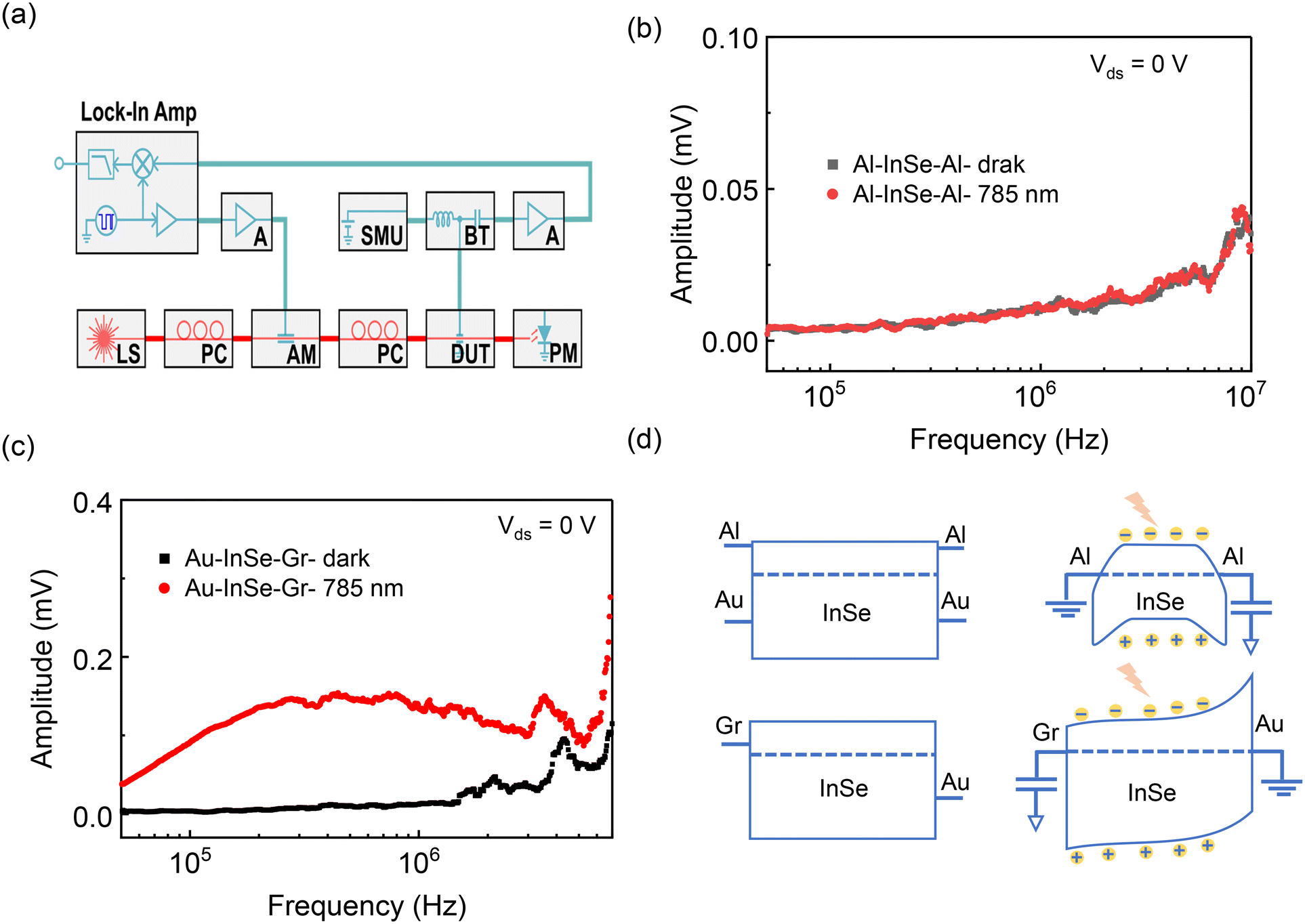 | ||
| Fig. 4 (a) Schematic representation of the experimental setup to measure the 3 dB cut-off frequency of the Au–InSe–Gr photodetector. Here, LS: laser source (785 nm), PC: polarization controller, AM: amplitude modulator, DUT: device under test, PM: power meter, A: amplifier, SMU: source meter unit, and BT: bias tee. (b and c) The response of the photodetectors during frequency sweeps of the symmetric and asymmetric devices, respectively. (d) Schematic representation of the band alignments of InSe with various electrodes (Al, Au, Gr) under (top) non-equilibrium and (bottom) equilibrium states (under illumination). | ||
The device's time-domain response was measured to evaluate its reaction to modulated light, as shown in Fig. S3.† In our measurements, a sinusoidal input was used to characterize the response. While sine waves offer valuable frequency-domain insights, they do not allow direct extraction of response speed metrics, such as rise and fall times, which are typically obtained using a step-function optical signal (e.g., a square wave). The transition times in a square wave excitation facilitate a direct assessment of the system's temporal resolution. Therefore, to evaluate the device's speed, we rely on frequency-domain analysis, where the 3 dB bandwidth provides an estimate of the response time.
To validate the device's response at 0 V, the frequency responses of InSe devices with symmetric and asymmetric contacts were measured under dark and illuminated conditions. The device with symmetric contacts exhibited similar behavior under both conditions (see Fig. 4b). In contrast, the device with asymmetric contacts demonstrated a clear distinction between the responses in the dark and under illumination, as shown in Fig. 4c.
In the symmetric configuration, the energy bands remain flat under equilibrium conditions, as shown in the upper sections of Fig. 4(d). Under light illumination, photogenerated carriers rely on diffusion to reach the contacts due to the absence of a built-in electric field. This diffusion-driven transport is inherently slow, resulting in ohmic electrical behavior and an inability to exhibit a measurable 3 dB cut-off frequency response at zero bias. In the asymmetric configuration, under equilibrium conditions (Fig. 4d, bottom sections), the energy bands bend at the graphene–InSe interface, creating a built-in electric field that facilitates carrier separation and transport. Under light illumination, this built-in electric field enables a drift-dominated transport mechanism that rapidly separates photogenerated carriers, reducing recombination losses and enhancing carrier mobility. The use of graphene as a contact further reduces resistance and enhances charge collection efficiency, resulting in a faster response time and a measurable 3 dB cut-off frequency.
Fig. 5(a) illustrates the measured 3 dB cut-off frequency of approximately 2.5 MHz at 0 V, corresponding to a response time (τr = 0.35/f3dB) of 140 ns. Notably, the device exhibits a response to RF signals up to 0.1 GHz, significantly outperforming other self-driven photodetectors (typically operating at ∼kHz levels).6 M. Dai et al. reported a similar Au–InSe–Gr structure, where the response times for vertical and lateral configurations were 235 ns and 0.107 ms, respectively.22 Despite the structural similarities, our device demonstrates a faster response time of 140 ns. This improvement is likely due to our fabrication approach, which avoids photoresist-based lithography and thus preserves the intrinsic properties of InSe. Given the surface sensitivity of 2D materials, fabrication techniques play a crucial role in determining device performance.
 | ||
| Fig. 5 (a) The measured 3 dB cut-off frequency of the Au–InSe–Gr device under 0 V, forward bias (positive voltage) and reverse bias (negative bias). (b) Measured noise-equivalent power (NEP) (black squares) and specific detectivity (D*) (red circles) as a function of illuminated optical power. | ||
The influence of bias voltage on the frequency response was further analyzed. As shown in Fig. 5(a), the 3 dB cut-off frequency increases from 2.5 MHz to 3.2 MHz when the bias voltage is raised from 0 V to +4 V. Under forward bias, the electric field across the Schottky junction is reduced, causing a narrowing of the depletion region. This decreases the transit time of photogenerated carriers due to their shorter drift path, resulting in an increased carrier drift velocity and improved response speed.
Conversely, the electric field across the depletion region is enhanced under reverse bias, broadening the depletion region. While this accelerates the drift velocity of carriers due to the stronger electric field, the increased depletion region width elongates the transit time for carriers to traverse the junction, leading to a slower overall response. The cut-off frequency drops to 1.3 MHz when the bias voltage is reduced to −4 V. Additionally, reverse bias can introduce enhanced carrier trapping and recombination effects within the depletion region, further limiting the device's response speed. These observations underscore the critical role of carrier transit time and the applied electric field in determining the photodetector's frequency response.
However, the relatively small change in speed with bias voltage is likely limited by factors such as carrier trapping and recombination, and contact resistance. The frequency response of photodetectors can be further improved by optimizing the thickness of the active layer, modifying the device configuration (e.g., vertical geometry), and by reducing the spacing between electrodes. In the current lateral device, photogenerated carriers must travel a relatively long distance of 30 μm to reach the electrodes, which limits response speed. In contrast, a vertical stack or a small-distance lateral device shortens the carrier transit path, leading to significant performance improvements. The carrier transit time (τt) in a vertical and lateral device is given by

| τRC = RLC |
It is worth mentioning that the measured response time (140 ns) surpasses the previously reported self-driven InSe photodetector response time despite the relatively long device channel length of 30 μm. In Table 1, we compare the response times of various self-driven photodetectors. The data points in the comparison table are extracted from recent reports on self-driven photodetectors based on different 2D materials and operating mechanisms.8,14,23–33 Furthermore, we measured the 3 dB cut-off frequency of the symmetric Al–InSe–Al device for comparison. The maximum measured cut-off frequency was 0.7 MHz at a bias of 3 V (see ESI Fig. S4†).
| Device | Type | Response time | Responsivity | Ref. |
|---|---|---|---|---|
| 2D MoS2 diodes with geometrically asymmetric contact areas | Geometrically asymmetric | 0.8 ms | 490.3 mA W−1 @450 nm | 8 |
| InSe Schottky diode and Au plasmonic nanoparticle (NP) | Lateral | 23 ms | ∼100 mA W−1 @785 nm | 14 |
| Au–InSe–Gr- | Lateral | 107.1 μs | — | 22 |
| Schottky junctions of Au–MoS2–ITO | Vertical | 64 μs | 1 A W−1 @637 nm | 23 |
| Au–WSe2–ITO Schottky junction | Vertical | ∼50 μs | 0.1 A W−1 @637 nm | 24 |
| 50 mA W−1 @785 nm | ||||
| MLG/Si Schottky junction | Lateral | 100 μs | 29 mA W−1 @850 nm | 25 |
| Monolayer graphene/germanium Schottky junction | Vertical | 23 μs | 51.8 mA W−1 @1550 nm | 26 |
| Graphene/GaAs nanowire Schottky junction | Vertical | 71 μs | 1.54 mA W−1 @532 nm | 27 |
| Piezo-phototronic effect γ-InSe | Lateral | 20.3 μs | 198.2 mA W−1@650 nm | 28 |
| Gr/p-GaSe/n-InSe/Gr | p–n junction | 1.85 μs | 21 mA W−1 @470 nm | 29 |
| p-GaTe/n-MoS2 | p–n junction | 10 ms | 1.36 A W−1 @633 nm | 30 |
| p-WSe2/n-MoS2 | p–n junction | 1 μs | 10 mA W−1 @532 nm | 31 |
| Few-layer BP | PEC type | 0.5 s | Simulated sunlight 0.1 M KOH | 32 |
| Few-layer Bi2S3 | PEC type | 0.1 s | 8.9 mA W−1@365 nm, 0.1 M KOH | 33 |
| Au–InSe–Gr | Lateral | 140 ns | 50 mA W−1 @785 nm | This work |
For any photodetector, the detection limit is determined by the noise-equivalent power (NEP), given by NEP = √(total noise)/R.34 This represents the incident power at which the signal power equals the dark current noise. In the case of the self-biased InSe photodetector, its sensitivity is primarily constrained by the total noise current (in) of the device. The noise in a photodetector arises mainly from the thermal noise (Johnson–Nyquist noise) (inJ = (√4kBTΔf/R0), shot noise (ins = √2e(Id + Iph)Δf), and the 1/f noise (i1/f = k1(IbΔf)/fa),34 where kB is the Boltzmann constant, T is the temperature, Δf is the measured bandwidth, and R0 is the resistance, while k1, a, and b are coefficients related to the fabrication process, material properties, and specific photodetector structure, respectively. At high signal frequencies (>1 kHz), the total noise current is primarily dominated by shot noise and Johnson noise. The experimentally measured shot noise and thermal noise are presented in Fig. S5(a).†
Next, the calculated NEP based on our measurements at a bias voltage of 0 V is shown in Fig. 5(b). The NEP at Vds = 0 V under illumination power of 0.25 μW is found to be approximately 2.37 pW/√Hz, demonstrating the ability to detect NIR radiation at the pico-watt level. For normal-incidence photodetectors, the specific detectivity (D*) is also widely used, defined as D* = √ΔfA/NEP, where A is the detector's illuminated area and the unit of D* is Jones (1 Jones = 1 cm Hz1/2 W−1).34 The calculated D* is also provided in Fig. 5(b). Finally, the prepared devices were tested under continuous periodic light pulses for 260 minutes (see Fig. S6†), and the measured photocurrent at Vds = 0 V remained consistent, demonstrating the device's stability under ambient conditions.
Conclusion
In summary, we demonstrate a high-performance, self-driven photodetector based on an asymmetric graphene–InSe–gold (Gr–InSe–Au) metal–semiconductor–metal (MSM) architecture. Utilizing a dry-transfer fabrication method, we achieve clean van der Waals interfaces between InSe and the electrodes, effectively suppressing Fermi-level pinning—one of the key limitations in 2D material-based devices. The photodetector delivers a notable responsivity of 57.15 mA W−1 under zero external bias, coupled with an ultralow dark current (∼10−11 A) and a fast response time of 140 ns. Moreover, the device exhibits excellent linearity with respect to incident light power density, making it well-suited for seamless integration with low-power signal processing circuits in next-generation optoelectronic systems.Data availability
Requests for data and materials should be addressed to SRT.Conflicts of interest
The authors declare no competing financial and non-financial interests.Acknowledgements
This work was supported by the NYUAD Research Enhancement Fund, NYUAD Center for Cyber Security, and NYUAD Center for Smart Engineering Materials. The authors are thankful to the NYUAD Core Technology Platform Facility (CTP) and NYUAD Photonic Research Lab for their support with analytical, material characterization, device fabrication, and testing. The authors are also grateful to the instrumentation research scientist Dr. Mohamed Ettabib from NYUAD CTP, for his help and support in the photonics lab.References
- T. Ma, N. Xue, A. Muhammad, G. Fang, J. Yan, R. Chen, J. Sun and X. Sun, Micromachines, 2024, 15, 1249 CrossRef PubMed.
- M. V. Sulleiro, A. Dominguez-Alfaro, N. Alegret, A. Silvestri and I. J. Gómez, Sens. Bio-Sens. Res., 2022, 38, 100540 CrossRef.
- J. Cheng, C. Wang, X. Zou and L. Liao, Adv. Opt. Mater., 2019, 7, 1800441 CrossRef.
- M. Liu, J. Wei, L. Qi, J. An, X. Liu, Y. Li, Z. Shi, D. Li, K. S. Novoselov, C.-W. Qiu and S. Li, Nat. Commun., 2024, 15, 141 CrossRef CAS PubMed.
- A. Liu, X. Zhang, Z. Liu, Y. Li, X. Peng, X. Li, Y. Qin, C. Hu, Y. Qiu, H. Jiang, Y. Wang, Y. Li, J. Tang, J. Liu, H. Guo, T. Deng, S. Peng, H. Tian and T.-L. Ren, Nano-Micro Lett., 2024, 16, 119 CrossRef PubMed.
- H. Qiao, Z. Huang, X. Ren, S. Liu, Y. Zhang, X. Qi and H. Zhang, Adv. Opt. Mater., 2020, 8, 1900765 CrossRef CAS.
- J. Zhang, Z. Hu, Q. Yang, S. Sun, F. Liu, H. Xu, X. Wang, Y. Zhao, N. Zhou, G. Dong, H. Zhang, R. Yang, L. Wang, W. Hu and X. Li, Adv. Mater., 2025, 37, 2410275 CrossRef CAS PubMed.
- A. Abnavi, R. Ahmadi, H. Ghanbari, M. Fawzy, A. Hasani, T. De Silva, A. M. Askar, M. R. Mohammadzadeh, F. Kabir, M. Whitwick, M. Beaudoin, S. K. O'Leary and M. M. Adachi, Adv. Funct. Mater., 2023, 33, 2210619 CrossRef CAS.
- S. R. Tamalampudi, Y.-Y. Lu, R. K. Ulaganathan, R. Sankar, C.-D. Liao, K. M. Boopathi, C.-H. Cheng, F. C. Chou and Y.-T. Chen, Nano Lett., 2014, 14, 2800–2806 CrossRef CAS PubMed.
- D. A. Bandurin, A. V. Tyurnina, G. L. Yu, A. Mishchenko, V. Zólyomi, S. V. Morozov, R. K. Kumar, R. V. Gorbachev, Z. R. Kudrynskyi, S. Pezzini, Z. D. Kovalyuk, U. Zeitler, K. S. Novoselov, A. Patanè, L. Eaves, I. V. Grigorieva, V. I. Fal'ko, A. K. Geim and Y. Cao, Nat. Nanotechnol., 2017, 12, 223–227 CrossRef CAS PubMed.
- Y. Wang, H. Wang, S. M. Gali, N. Turetta, Y. Yao, C. Wang, Y. Chen, D. Beljonne and P. Samorì, Adv. Funct. Mater., 2021, 31, 2103353 CrossRef CAS.
- W. Luo, Y. Cao, P. Hu, K. Cai, Q. Feng, F. Yan, T. Yan, X. Zhang and K. Wang, Adv. Opt. Mater., 2015, 3, 1418–1423 CrossRef CAS.
- X. Yang, X. Liu, L. Qu, F. Gao, Y. Xu, M. Cui, H. Yu, Y. Wang, P. Hu and W. Feng, ACS Nano, 2022, 16, 8440–8448 CrossRef CAS PubMed.
- M. Dai, H. Chen, R. Feng, W. Feng, Y. Hu, H. Yang, G. Liu, X. Chen, J. Zhang, C.-Y. Xu and P. Hu, ACS Nano, 2018, 12, 8739–8747 CrossRef CAS PubMed.
- S. R. Tamalampudi, J. E. Villegas, B. Paredes, G. Dushaq and M. S. Rasras, CLEO: Science and Innovations, Technical Digest Series, 2023, Optica Publishing Group, Integrated SiN/InSe Waveguide Photodetector for O-band Applications, paper JW2A.41 Search PubMed.
- S. R. Tamalampudi, J. E. Villegas, G. Dushaq, R. Sankar, B. Paredes and M. Rasras, Adv. Photonics Res., 2023, 4, 2300162 CrossRef CAS.
- C. Patil, H. Dalir, J. H. Kang, A. Davydov, C. W. Wong and V. J. Sorger, Appl. Phys. Rev., 2022, 9, 1931 Search PubMed.
- L. Qi, M. Che, M. Liu, B. Wang, N. Zhang, Y. Zou, X. Sun, Z. Shi, D. Li and S. Li, Nanoscale, 2023, 15, 13252–13261 RSC.
- Q. Zhao, W. Wang, F. Carrascoso-Plana, W. Jie, T. Wang, A. Castellanos-Gomez and R. Frisenda, Mater. Horiz., 2020, 7, 252–262 RSC.
- J. Jiang, Y. Wen, H. Wang, L. Yin, R. Cheng, C. Liu, L. Feng and J. He, Adv. Electron. Mater., 2021, 7, 2001125 CrossRef CAS.
- C. Yang, G. Wang, M. Liu, F. Yao and H. Li, Nanomaterials, 2021, 11, 2079 CrossRef PubMed.
- M. Dai, H. Chen, F. Wang, M. Long, H. Shang, Y. Hu, W. Li, C. Ge, J. Zhang, T. Zhai, Y. Fu and P. Hu, ACS Nano, 2020, 14, 9098–9106 CrossRef CAS PubMed.
- F. Gong, H. Fang, P. Wang, M. Su, Q. Li, J. C. Ho, X. Chen, W. Lu, L. Liao, J. Wang and W. Hu, Nanotechnology, 2017, 28, 48 CrossRef PubMed.
- M. Luo, F. Wu, M. Long and X. Chen, Nanotechnology, 2018, 29, 444001 CrossRef PubMed.
- P. Lv, X. Zhang, X. Zhang, W. Deng and J. Jie, IEEE Electron Device Lett., 2013, 34, 1337–1339 CAS.
- L.-H. Zeng, M.-Z. Wang, H. Hu, B. Nie, Y.-Q. Yu, C.-Y. Wu, L. Wang, J.-G. Hu, C. Xie, F.-X. Liang and L.-B. Luo, ACS Appl. Mater. Interfaces, 2013, 5, 9362–9366 CrossRef CAS PubMed.
- Y. Wu, X. Yan, X. Zhang and X. Ren, Appl. Phys. Lett., 2016, 109, 18 Search PubMed.
- M. Dai, H. Chen, F. Wang, Y. Hu, S. Wei, J. Zhang, Z. Wang, T. Zhai and P. Hu, ACS Nano, 2019, 13, 7291–7299 CrossRef CAS PubMed.
- F. Yan, L. Zhao, A. Patanè, P. Hu, X. Wei, W. Luo, D. Zhang, Q. Lv, Q. Feng, C. Shen, K. Chang, L. Eaves and K. Wang, Nanotechnology, 2017, 28, 27 CrossRef PubMed.
- S. Yang, C. Wang, C. Ataca, Y. Li, H. Chen, H. Cai, A. Suslu, J. C. Grossman, C. Jiang, Q. Liu and S. Tongay, ACS Appl. Mater. Interfaces, 2016, 8, 2533–2539 CrossRef CAS PubMed.
- C.-H. Lee, G.-H. Lee, A. M. van der Zande, W. Chen, Y. Li, M. Han, X. Cui, G. Arefe, C. Nuckolls, T. F. Heinz, J. Guo, J. Hone and P. Kim, Nat. Nanotechnol., 2014, 9, 676–681 CrossRef CAS PubMed.
- X. Ren, Z. Li, Z. Huang, D. Sang, H. Qiao, X. Qi, J. Li, J. Zhong and H. Zhang, Adv. Funct. Mater., 2017, 27, 1606834 CrossRef.
- W. Huang, C. Xing, Y. Wang, Z. Li, L. Wu, D. Ma, X. Dai, Y. Xiang, J. Li, D. Fan and H. Zhang, Nanoscale, 2018, 10, 2404–2412 RSC.
- F. Wang, T. Zhang, R. Xie, Z. Wang and W. Hu, Nat. Commun., 2023, 14, 2224 CrossRef CAS PubMed.
Footnotes |
| † Electronic supplementary information (ESI) available. See DOI: https://doi.org/10.1039/d5nr00465a |
| ‡ These authors are equally first. |
| This journal is © The Royal Society of Chemistry 2025 |