
Single electron transistor based charge sensors: fabrication challenges and opportunities
Jency Rubia
J
 a,
Julaiba Tahsina
Mazumder
ab,
Arun B.
Aloshious
c and
Ravindra Kumar
Jha
*acd
a,
Julaiba Tahsina
Mazumder
ab,
Arun B.
Aloshious
c and
Ravindra Kumar
Jha
*acd
aNano Sensors & Devices Lab, Electronics and Electrical Engineering Department, Indian Institute of Technology Guwahati 781039, India. E-mail: jha@iitg.ac.in
bCentre of Excellence for Nanotechnology, Department of Electronics and Communication Engineering, Koneru Lakshmaiah Education Foundation, Vaddeswaram, Andhra Pradesh-522302, India
cDepartment of Electrical and Electronics Engineering, Indian Institute of Technology Guwahati 781039, India
dCentre for Intelligent Cyber-Physical Systems, Indian Institute of Technology Guwahati 781039, India
First published on 9th April 2025
Abstract
Measuring electric charge precisely is crucial in various fields including semiconductor device fabrication, particle physics, materials science, medical imaging, electrotherapy, electroplating, and electrolysis. It becomes even more demanding for quantum applications. Existing technology like voltmeters and electrometers are valuable tools, but limitations like low sensitivity, drift, and accessibility hinder their use in quantum applications. Researchers are addressing these issues by exploring new approaches like nanomaterial-based sensors with quantum mechanics for ultra-sensitive charge detection. The single-electron transistor (SET) achieves high sensitivity by controlling individual electron flow due to the Coulomb blockade principle and other quantum phenomena. Existing charge sensors have limited operation, as it is very challenging to detect very small changes in charge due to the continuous current flow. In contrast, SETs control the flow of individual electrons due to the discrete nature of flowing electrons. Furthermore, ultra-low power and highly reliable electronic components can be created by precisely controlling single electrons, which introduces a new era of miniaturized and energy-efficient electronics. In this review, the rudiments of SETs and the significance of material choice for a SET are highlighted. The nano-fabrication methods, leading to the development of next-generation ultra-sensitive and low-power quantum electronics are pointed out. The challenges and issues are incorporated into developing new ideas, approaches, and technologies for the field of quantum sensors. Finally, we discuss the future outlook and potential developments to accelerate the development of high-precision SET-based charge sensors for future research directions.
 Jency Rubia J | Jency Rubia J is a Postdoctoral Fellow in the Electronics and Electrical Engineering Department at IIT Guwahati, and an associated faculty member at Vel Tech University, Chennai. She holds a Ph.D. from Anna University with a patent in high-speed VLSI. Currently, as part of the Nano Sensor & Devices Group at IIT Guwahati, her research focuses on the cutting-edge field of quantum technology, specifically single electron transistors (SETs), quantum dots, and quantum sensors. |
 Julaiba Tahsina Mazumder | Julaiba Tahsina Mazumder received her Ph.D. in Electronics and Communication Engineering from the National Institute of Technology Silchar, India. She was working as an Institute Post-doctoral Fellow with the Nano Sensors and Devices Group, Electronics and Electrical Engineering Department, Indian Institute of Technology Guwahati, India. She has joined the Koneru Lakshmaiah Education Foundation as an Assistant Professor in the Electronics and Communication Engineering Department. Her research areas include solar cell materials, photodetector device fabrication, the design and development of electronic sensors, and density functional theory. |
 Arun B. Aloshious | Arun B. Aloshious (Member, IEEE) received his B.E. degree in electronics and communication engineering from Anna University, Chennai, India, in 2009, M.Tech. degree in electronics and communication engineering from the National Institute of Technology, Calicut, India, in 2011, and Ph.D. degree in electrical engineering from the Indian Institute of Technology Madras, Chennai, in 2020. Between 2020 and 2021, he was a Postdoctoral Research Associate with Duke University, Durham, NC, USA. He is currently an Assistant Professor with the Indian Institute of Technology Guwahati, Guwahati, India. His research interests include classical and quantum coding theory, quantum computation, information theory, signal processing, and communication. |
 Ravindra Kumar Jha | Ravindra K. Jha has been an assistant professor in the Electronics and Electrical Engineering Department at IIT Guwahati and associated faculty in the Centre for Intelligent Cyber Physical Systems, IIT Guwahati since 2021. He served as a scientist at the CSIR-Central Electronics Engineering Research Institute (National Laboratory of India) at Pilani, Rajasthan, India, in the Nano-Bio Sensors group and Microsystems Packaging Group before accepting his current position. Before that, he was with the Indian Institute of Science, Bengaluru, and the National Physical Laboratory, New Delhi, in various roles. His Nano Sensors & Devices Group, at IIT Guwahati, focuses on solid state and quantum sensors, flexible & sustainable sensors, breath biomarker detection, and additive manufacturing for electronics. |
Introduction
Quantum sensing is a rapidly growing area of science. It promises to greatly improve how we measure things, diagnose illnesses, and process information. This is because quantum sensors utilize quantum mechanics for precise measurements. Charge sensors detect electrical charge. When these charge sensors use quantum effects, they become quantum charge sensors. Single-electron transistors (SETs) are a prime example of quantum charge sensors, employing the Coulomb blockade effect for highly sensitive charge detection. These tiny devices can detect extremely small changes in electrical charge, more precisely than ever before. Previously, quantum point contacts (QPCs) and capacitive-based charge sensors were used for charge-sensing applications. All those existing sensors generally responded to the total electric field, not just the charge of a specific object. Single-electron transistors (SETs) address this challenge by providing charge detection at the single-electron level, offering enhanced sensitivity beyond the classical sensor. A detailed overview of the single-electron transistor (SET) device's evolution is presented in Table 1.| Aspect | 1980–1990 | 1990–2000 | 2000–2010 | 2010–2024 |
|---|---|---|---|---|
| Theory and modeling | • Early theoretical discussions on SET behaviour | • Refinement of SET models | • Advanced modeling techniques | • Comprehensive theoretical frameworks |
| • Exploration of quantum confinement effects | • QD energy level studies | • Room-temperature operation investigations | • Co-integration with CMOS explored | |
| Design and fabrication | • Initial SET designs based on the Coulomb blockade | • Improved fabrication techniques | • Electromigration-induced activation | • Co-integration with CMOS technology |
| • Fabrication challenges | • Nanoscale control of tunnel junctions | • Precise parameter evaluation | • Material choices for stability | |
| Advantages | • Potential for ultra-low power operation | • Compatibility with CMOS technology | • Room-temperature SETs demonstrated | • SET as a potential nano-device for futuristic applications |
| • Exploitation of quantum effects | • Enhanced performance at scaled nodes | • QD-based computing systems | • Heterogeneous 3D integration prospects | |
| Challenges and drawbacks | • Low current drivability | • Small voltage gain | • Noise susceptibility | • Seamless hybrid design trade-offs |
| • Sensitivity to background charges | • Cryogenic operation | • Stability issues | • Maintaining overall performance | |
| • Short-channel effects | ||||
| • Aggregation of non-idealities |
The single-electron effects will be crucial in almost any electronic device with dimensions below ∼30 nm, and this is considered a new physical basis for nanoscale digital circuits. The confinement of an electron can alter the number of energy levels and the bandgap of the semiconductor to provide a quantized flow of electrons. By accommodating these particles in a tiny space, their behaviour changes dramatically compared to bulk materials. If an electron is confined in three dimensions, it is called a quantum dot. The QD, which is also sometimes called an island of a SET, plays a key role in controlling electron movement. Because of this extreme confinement, the allowed energy levels become very discrete, almost like individual dots on a line. A QD exhibits unique optical and electrical properties and is being explored for applications in bioimaging,1,2 displays,3,4 photodetectors,5 photovoltaics, LEDs,6 solar cells,7 microscopy8 and quantum computing.9,10 Therefore, the degree of confinement influences the energy levels available to electrons. Also, it impacts various properties of the material, including electrical conductivity, mobility, mechanical, thermal, biocompatibility, chemical, and overall behaviour.
Nanomaterials can restrict electrons at the nanoscale; nanomaterials are essential for the functioning and promise of these devices. We can produce structures with specific quantum mechanical features, such as narrow channels or quantum dots, by modifying materials at the atomic scale. A fundamental idea of SET operation is controlled electron tunneling, made possible by nanomaterials with tiny insulating barriers. For a practical SET to operate, specific electrical properties, such as a high work function and low leakage current, are essential, and nanomaterials provide a means of obtaining these qualities.
The central island of SETs can be constructed using quantum dots created from materials like silicon or gallium arsenide, which enable exact control over electron tunneling. Certain kinds of carbon nanotubes (CNTs) can be utilized to make conducting channels perfect for regulated electron tunneling, with well-defined sizes and great purity. As the conducting island in SETs, single molecules with clearly defined energy levels provide the highest degree of miniaturization and the possibility of novel capabilities. Because of their capacity to confine electrons along a single dimension, narrow strips of graphene can display unique electrical properties appropriate for SET applications.11 Nanomaterials are crucial for advancing single-electron transistors (SETs). They enable the creation of extremely sensitive, low-power devices for a range of applications by addressing existing constraints such as temperature requirements, fabrication challenges, and integration issues. Some nanomaterials, such as graphene and carbon nanotubes, have special electrical characteristics that allow SETs to function at higher temperatures, even at room temperature. Since it eliminates the need for expensive cryogenic cooling systems, this is a major advancement since SETs become more viable for general usage. Nanomaterials thus have great power to revolutionize the discipline of single-electron transistors. Further investigation and advancement may result in extremely sensitive, low-power gadgets that find use in quantum computing, next-generation electronics, and ultra-sensitive sensors.
Measuring a single-electron charge, fundamental quantum technology is of paramount importance. Charge sensing is a crucial component for measuring single spins, single photons, and single molecules, leading to applications in single-electron charge, single-electron spin, photon–electron quantum interface, and bio-sensors.12 These SETs can detect when an electron has tunnelled from a source electrode to the drain (Fig. 1a). The sensitivity of the SET has been realized by the effect of coupling QDs to the source, drain, and gate electrodes. Thus, the number of electrons in the dot can be determined by tuning the gate voltage. The SET's sensitivity is measured from current–voltage observations of the device.13 Under specific gate–voltage settings, the conductance via the (SET) sensor is susceptible to the electrostatic environment. Single-electron charge sensing is made possible by single-electron charging in the QD, which dramatically alters the sensor's (SET) conductance because of the SET's proximity to the QD. Real-time detection of single-electron tunneling events is made possible by this technology, which functions even in cases where QD conductance is too tiny to measure.14 Furthermore, by converting other physical quantities into electron charge, this real-time charge sensing enables the measurement of other physical quantities: spin-dependent tunneling events have been used to readout single-electron spin,15–17 and single-photon detection has been demonstrated by detecting single photoexcited electrons.18,19 A few investigations on charge sensing for vertical QDs,20 carbon nanotube QDs,21 and nanowire QDs22,23 have also been published. These research efforts include either positioning a sensor (SET) close to a QD or linking a sensor and a QD via a floating gate.
 | ||
| Fig. 1 a. Schematic diagram of quantum dot tunneling. b. Schematic diagram of a tunnel junction. c. Illustration of the Coulomb blockade system and its energy band structure with filled and empty levels (bottom) (this figure has been reproduced from ref. 41 with permission from the American Physical Society copyright 2024). d. Schematic diagram of the 2D charge stability plot (this figure has been reproduced from ref. 42 with permission from Springer Nature copyright 2024). e. Slope calculated from the charge stability diagram. | ||
A SET charge sensor is ideal for applications demanding ultra-high sensitivity for single-electron detection. The SET charge sensor finds use in areas like QD characterization, biomolecule sensing with high specificity, and real-time monitoring of single-electron processes.24 The SET-based charge sensor can be used as a bio-sensor as well.25 The gate electrode of a SET can be functionalized with biorecognition molecules like antibodies or enzymes. These molecules specifically bind to target biomolecules (e.g., proteins, DNA) present in a sample.26 When a target biomolecule binds to the recognition element, it alters the local electrical environment around the SET gate. This change in charge can be detected by the SET as a shift in its current flow.
Researchers have focused on SETs because of their special qualities and potential for unprecedented applications. One of a SET's primary features is its extreme sensitivity.27 This is made feasible by the incredibly sensitive detection and measurement of minute changes in charge made possible by quantum physics. They are therefore ideal for high-precision uses such as biosensing and QD research. Biosensors can detect the presence of biomolecules like proteins or DNA (deoxyribonucleic acid) by measuring the tiny changes in charge that occur when these molecules bind to the SET's surface.28 SETs can probe the quantum properties of individual electrons confined within tiny semiconductor structures called QDs, leading to quantum dot research.29 Furthermore, a SET works on the premise of directing the flow of single electrons, in contrast to ordinary transistors that deal with millions of electrons. The basic informational elements of quantum computing are quantum bits, or qubits; SETs are appealing building blocks for their development. Encoding and processing quantum information depends on their capacity to control single electrons. This will lead to manipulation in a quantum computer and by integrating SETs with molecules exhibiting specific electronic properties, researchers can create novel devices with functionalities beyond conventional electronics. This is known as molecular electronics.30,31
The small size and scalability of SETs make them attractive for building ultra-miniaturized electronic devices. This feature of scalability can be used for high-density integrated circuits. SETs hold promise for creating powerful and compact integrated circuits with a much higher density of transistors compared to conventional devices. Also for nanoelectronics, where researchers aim to create electronic devices on the atomic and molecular scale. Due to their low current operation, SETs are inherently energy-efficient, and achieving room-temperature operation would enable their use in practical low-power applications. SETs could be used to build low-power logic circuits for applications where energy consumption is a major concern. Recent research in SET synthesis focuses on improving fabrication techniques to achieve room-temperature functionality and miniaturization for large-scale applications. Researchers are creating reconfigurable SETs that can switch between different operational modes. This allows for more versatile devices with potential applications in low-power, reconfigurable logic circuits.32 As researchers pack more SETs onto a chip, reducing their size becomes crucial. New synthesis approaches aim to optimize the layout of SET arrays to minimize their overall width while maintaining functionality.33 The scientific community is actively striving to overcome obstacles including room-temperature operation and fabrication complexity, even though these remain. SETs are a fascinating topic of research with great potential to transform several technical domains because of their special qualities and their uses. Therefore, this investigation seeks to explore SET fabrication, operational concepts, and several uses, thus revealing their promise as next-generation quantum sensors. We show how to construct high-performance SET-based sensors able to push the limits of measurement accuracy by analyzing current developments in nano-fabrication methods.
In this review, we discuss the evolution of SETs in terms of devices and the selection of suitable materials and SET-based quantum devices as sensors. Also, we discuss the fundamental concepts of SETs, such as tunnel junctions, the Coulomb blockade effect, QDs, Coulomb diamonds, and advancements in fabrication and characterization strategies. We then outline the challenges and problems of SETs, with particular attention paid to integration, noise, and operational conditions. Finally, in order to inspire hope and optimism, we highlight SETs’ bright future and their potential as a research avenue for SET candidates.
Fundamentals of SETs
Single-electron transistor operation
A single-electron transistor (SET) fundamentally consists of a small conductive quantum dot (QD) connected to a gate electrode via a capacitive coupling and to source and drain metallic leads through thin tunneling junctions (Fig. 1a). The operational principle of a SET relies on the Coulomb blockade effect. Due to electrostatic repulsion between electrons within the confined space of the QD, significant energy is required to add an additional electron. This phenomenon, which arises from the discrete nature of charge, dictates the conductance behavior of the SET. Specifically, the energy required to add or remove a single electron is given by e2/2C, where ‘C’ represents the total capacitance of the QD.34 The tunneling junctions, acting as insulating barriers, prevent classical electron flow. However, quantum mechanical resonant tunneling allows electrons to traverse these barriers when their energy aligns with the discrete energy levels of the QD. The quantum dot, by storing charges, behaves as a capacitor, similar to a metal–insulator–metal structure (Fig. 1c). Consequently, controlling the gate voltage enables precise manipulation of the QD's energy levels, thereby regulating electron tunneling and the SET's conductance.The SET has some requirements for charge to affect it and we call this the “Orthodox theory”.35 It is necessary for the capacitance to be lower than the energy needed to charge one electron (i.e.) Ec = e2/2C where Ec is the electrostatic energy of charge and C is the capacitance.36 This is regarded as the prerequisite for the measurement of single electron tunneling. Since the capacitance and size of the QD are directly correlated, the electrostatic energy of the charge can be controlled.37 The maximal charging energy of the QD can only be retained at a size of roughly less than a few nanometers. However, tunneling electrons from the source to the QD is complex because of the “Coulomb blockade” principle. Hence, a tunneling electron requires more energy to tunnel through the barrier.
The second requirement is that charging and discharging of the QD should have a finite time. The rate (Δt) at which the capacitance builds up charge or discharges is proportional to RTC. Because of the tunnel resistance, the charging and discharging of QDs can take place over an exponentially long time. This means that even a small increase in tunnel resistance can significantly increase the time it takes to charge or discharge the QD. Then, the SET device has to be operated in a very low temperature (below 4 K) environment, which is an essential requirement,38 because thermal energy should not be involved in the electron transport mechanism. Otherwise, temperature controls electron transport, which is not desired. Tunnel resistance, which must be kept at a high level, is a particular criterion that must be met to overcome the uncertainty principle. We know that the uncertainty principle is a fundamental limitation of quantum mechanics. It states the inherent limitation of knowing the position and momentum of a particle with perfect accuracy simultaneously.39
| ΔEΔt ≥ h |


| RT > 51.6 kΩ |
From the above relationships, a high tunnel resistance (RT) can reduce the current fluctuations in an SET, which leads to a smaller uncertainty in the measurement of the charge on the QD. However, it does not eliminate the limitation of the fundamental uncertainty principle.
The Coulomb diamond (charge stability diagram)
The charge stability diagram shows how the quantity of electrons on the SET QD relates to its operational parameters and depicts the QD's energy state. The charge stability diagram is a 2D graph that plots the conductance (or current) through a single-electron transistor (SET) as a function of the gate voltage, Vg, and the bias voltage, Vds, revealing the Coulomb blockade regions and conductance peaks. This plot contains a diamond-shaped region in the middle of the graph; hence it is called a Coulomb diamond.40 Every diamond signifies a specific quantity of electrons occupying the QD, which is known as the charge state, Q0. The boundaries of these diamonds mark the points at which adding or removing an electron becomes energetically unfavourable. The characteristics of QDs such as the charging energy needed to add or remove an electron can be analysed using the size, shape and position of these diamonds. Electrons cannot pass through the QD unless the electrodes have a specific chemical potential of μ, where μ represents the average energy per electron in a reservoir (electrode) connected to the QD. The alignment of the chemical potential (μ) of the QD with regard to the potentials of the source, μs, and drain, μd, has a significant impact on the electron transfer process. Consider electron transport through the QD, not including the excited states of the QD and level-broadening behaviour (Fig. 1d). For the condition of a chemical potential of μdot = μs = μd, the respective gate voltage is Vg = 0.As the charges inside these regions are locked to N or N + 1, the charge stability diagram's grey-coloured zone provides the Coulomb blockade region. The white colour of the QD represents the ability of electrons to tunnel into and out of it. However, due to a smaller number of electrons available at the QD, it is always better to determine conductance, dI/dV, than current, I, for a more sensitive measurement. So, even tiny changes in gate voltage (dV) can lead to significant changes in conductance, making it easier to detect and analyse the behaviour of the SET.43 So, the current I can be substituted with conductance dI/dV for measurement. Red and blue lines are thus the only visible indication of the change in current I. The red and blue lines indicate that the QD's chemical potential is equal to that of the source and drain (Fig. 1d). The chemical potential of the QD is higher than the source and drain leads at the initial zero bias voltage, Vds = Vs = Vd = 0, and Vg < 0. Consequently, there is a charge fluctuation between the N and N + 1 states and the electron cannot be transferred because the SET is in the off state (Fig. 1d). Raising Vg to zero will therefore suppress the chemical potential level of the QD to the source and drain levels. Now, the electrons tunnel into and out of the QD from both the leads (source and drain), which results in charge fluctuations in the N and N + 1 states. The term “charge degeneracy point” refers to this particular operational zone (Fig. 1d). The QD's chemical potential is lowered from any of the leads by increasing the gate voltage even further. As a result, the SET is in the off position but the QD has N + 1 electrons. When the charge inside the diamond is fixed, the SET is in the Coulomb blockade phase because it would require energy to overcome the Coulombic contact force with an extra electron. Current is observed even when Vds ≠ 0, and the chemical potential shifts between the drain and source, within the energy window of μs − μd = eVds, if the gate voltage is Vg ≠ 0. Turning the SET on or off by crossing the red lines causes a conductance ridge to form along the line. The equivalent circuit can be used to calculate the slope, which is given by −Cg/(Cg + Cs), by setting the potential difference between the QD and source to zero (Fig. 1e). A blue-coloured conduction regime may emerge if the chemical potentials of the drain and the QD line up (Fig. 1e). Setting the potential difference between the drain and the QD to zero enables computation of its slope, Cg/Cd, which has the opposite sign. Consequently, the SET is in a Coulomb blockade in the grey zone while the transistor is on inside the white region.
Single electron tunneling
The tunneling effect can be measured when the tunnel junctions are made too small and at low temperatures. If the existing charge (Q) at the junction is greater than half an electron's positive charge (+e/2), an electron can tunnel the barrier because ‘e’ is subtracted from the charge ‘Q’, thereby reducing the electrostatic energy of the QD. Similarly, the charge Q at the junction is smaller than −e/2, so an electron can tunnel because ‘e’ is added to the charge ‘Q’, thereby reducing the energy of the QD. But, in the range −e/2 < Q < +e/2, the electrostatic energy of the QD will be increased. Hence, in this region electrons cannot flow and this range is called the Coulomb blockade.44To observe the tunneling effect, the tunnel junction is connected to a constant current source. Initially, the system is in the Coulomb blockade region when the charge Q is zero, hence tunneling is forbidden. As a result, the source current begins to increase and exceeds +e/2. Then sufficient energy can pass one electron through the tunnel junction, and then again, the charge Q is greater than −e/2. Consequently, the system once more reaches the zone of the Coulomb barrier, making tunneling impossible. The charge Q increases until it attains +e/2 as the current stores positive charges in the junction at a consistent rate. After that, it repeats the procedure once again, which leads to the development of single-electron tunneling oscillations. The SET's oscillation frequency is calculated by dividing the current by the basic unit of charge (e).45 The concept of single electron tunneling can be explained using water leaking from a faucet for a better understanding (Fig. 2).37 The interface between an electrode and the insulator has no charge initially. As the electrons starts to flow onto the electrode, charges are stored on the conductor. When enough charges reach the electrode, an electron passes to the insulator and thereby reduces the surface charge. The process will repeat again if the charge is refilled. However, as the size of the droplet can vary in size, the quantity of tunneling charge is quantized and it is always equal to e.46 Thus, a time correlation of the tunneling events takes the form of coherent SET oscillations with the frequency.
 | ||
| Fig. 2 Single-electron tunneling through a small junction resembles a water droplet falling from a faucet (this figure has been reproduced from ref. 37 with permission from Scientific American copyright 2024). | ||
But the gate voltage, Vg, controls the energy required for the addition of the electron to a QD. Thus, the electrostatic energy of a charge Q on a QD under the influence of Vg is given as,
| E = QVg + Q2/2C | (1) |
The first term of eqn (1) represents an attractive interaction between negatively charged Q and a positively charged gate electrode. The second term defines the repulsive force between charges on the QD.
The single tunnel junction provides insights into the behaviour of a simple SET (Fig. 3a, top). When an insignificant drain–source bias voltage (Vds) is applied, the left lead has a greater Fermi energy level than the right lead by eVds. The energy level eVds represents a unit of energy convenient for describing the energy levels in quantum systems that refers to the product of the electron charge (e) and the source–drain bias voltage (Vds). It represents the potential energy difference experienced by an electron due to the applied voltage between the source and drain electrodes of the SET. Afterward, the current that is passing through the tunnel intersection can be written as,
 | (2) |
 is the tunnel barrier transmission coefficient at energy E, and f(E) is the Fermi–Dirac distribution function. In this expression, the term ‘−f(E − eVds)’ refers to electron tunneling from the right lead to the left lead. For a metallic QD, the coefficient
  is a slowly varying function based on its energy E. Thus, determining the conductance of the system also varies slowly with bias voltage Vds. This means that as the energy level (E) changes slightly, the number of available states (
 ) does not change dramatically. In simpler terms, there are always plenty of energy states available for electrons in the metal over a small energy range. As a result, the overall conductance of the SET through the metallic leads changes gradually with Vds. In semiconductors, the density of states can change more abruptly with energy. This can lead to sharper variations in conductance with changes in Vds, offering more control over the current flow. Next, consider the SET with two tunnel barriers in series with a large metal QD between them (Fig. 3a, right). If the metallic QD is larger in size, the size of the tunnel barriers will be reduced. Hence, an electron can easily pass into the QD and off of the QD. Thus, the controllability over tunneling will get lost. In another case, consider a small metallic QD in between both tunnel junctions, the size of the tunnel barriers will not get reduced. So, an electron cannot tunnel easily through the barrier. As a result, the conductance in a SET might vary dramatically depending on the size of the QD. The energy of the system can be raised by charging the capacitance of the tunnel junctions, which occurs when an electron moves from the source to the drain. Traditionally, the charging energy is calculated as U = e2/2C, where C represents the total capacitance of both junctions.31 If the metal QD is small, the capacitance value is also low, allowing charging energy U to surpass the value of ‘kT’. The small size of the metal QD can be made possible by designing the capacitance of the sphere to be on the order of 10−16 farad since the capacitance is directly proportional to the size of the metal QD (C = εA/d). A very small capacitance can provide a charging energy on the order of meV (Fig. 3a, right and bottom) and the charging energy creates a gap in the transmission spectrum,
  . Adding or withdrawing a single electron from the QD needs an energy of U/2. Furthermore, no current will flow at voltages for which eV ≥ U and temperatures for which kT ≥ U, which describes the Coulomb blockade of tunneling.
 | ||
| Fig. 3 a. Tunnel barrier between two metal electrodes and their respective energy band structures in the context of single electron tunneling. b. A tunnel barrier junction between two electron reservoirs 1 and 2 (top); tunnel barrier energy landscape using Fermi energies (bottom). | ||
Charging effects on SETs
The inherent quantization of electric charge, whereby it exists in discrete multiples of elementary charge, is a fundamental principle. Within confined systems, such as the island of a single-electron transistor (SET), energy levels are similarly quantized, restricting electrons to specific, discrete energy states. As aforementioned, an additional energy of e2/2C is required to add an electron to the QD due to the Coulomb blockade principle. Eqn (1) represents the parabola of energy as a function of charge and the minimum energy occurs when the charge on the capacitor (tunnel junction) is Q0 = −CVg. From the concept of elementary charge e, the capacitance, C, of a capacitor can be expressed in terms of the number of electrons, N, that flow onto the capacitor and the voltage applied across it (i.e.), C = Ne/Vg. Hence, Q0 becomes . At controlling charge state Q0 = −Ne, the energy of the system is at a maximum. Hence a greater energy difference is required to tunnel an electron from the source to the drain. If the controlling charge state increases further to Q0 = −(N + 1/4)e, the energy of the system drops slowly and requires less energy to make an electron tunnel. Further increasing the controlling charge state to Q0 = −(N + 1/2)e will lead to a reduction in the energy of the system and make an electron transition with much less energy (Fig. 4a). These points are called charge degeneracy points because both energy states N + 1 and N have the same energy, which makes an electron fluctuates between N and N + 1. Finally, at the controlling charge state of Q0 = −(N + 3/4)e, the energy of the system again increases and it is difficult to make the transition unless or until the required energy is provided to make a tunnel. Thus, these iterations make an electron transition from the N state to the N + 1 state. As the controlling charge state (Q0) increases steadily, a point of charge transition (degeneracy point) and a peak in conductance are observed repeatedly. These occur at specific voltage intervals, corresponding to the energy needed to add a single electron to the artificial atom (e2/2C).47
 | ||
| Fig. 4 a. Total energy and charge function in relation to four distinct gate voltage levels (this figure has been reproduced from ref. 31 with permission from AIP Publishing copyright 2024). b. Coulomb blockade I–V characteristics of a single-electron transistor (SET) with tunnel junctions. | ||
The potential energy in the tunnel junction (Fig. 3b) can be affected by the tunnel junction capacitance. This can be understood from two limiting cases. First, the junction is connected to the voltage source with low internal resistance. The second case denotes the connection of the current source to a tunnel junction with high internal resistance. Initially, the voltage source or electrochemical potential difference of Δμ = eV is applied to the tunnel junction.48 If the tunnel junction has a resistance of Rt = 1/Gt and capacitance C, the metal system builds up charges +Q and −Q at the two sides of the barrier. Consequently, the accumulated charges +Q and −Q effectively result from a shift in the average positions of the electrons on the two sides of the barrier. This shift can lead to a continuously variable polarisation charge, which is linearly dependent on the difference in electrochemical potential.49 This means the charge is related to the capacitance of the tunnel barrier i.e. Q = CV. However, under these conditions, the tunnel resistance is Rt ≫ h/2e2, so any charge that would tunnel will be quantised in units ‘e’.
In order to examine the charges’ time-dependent behaviour on a single junction, the current source must be linked to the tunnel junction. The current source has a very large internal resistance, Rs, and so it forces a constant current, I, through the junction. If a single electron with charge −|e| tunnels through the barrier, the charge changes from Q to Q − |e|. Thus, the electrostatic potential changes from Uinitial before tunneling to Ufinal after the tunneling event and can be given as
 | (3) |
But at zero temperature (T = 0 K), tunneling will occur only if ΔU < 0, i.e. whenever the system may enter a lower energy state, and this condition gives Q > |e|/2 or V = Q/C > |e|/2C. If tunnel resistance Rt is in the infinite range, the electrons tunneling across the barrier cannot take place. This implies that the constant current linearly increases charge Q with time. However, if Rt is finite, tunneling is allowed whenever the second condition is met. Thus, the total charge Q oscillates between approximately −e/2 and e/2 and so the voltage is between −e/2C and +e/2C. This indicates that the voltage at the junction has the opposite polarity for half of the oscillation.50 Consequently, the sawtooth oscillatory behaviour of the charge has an average time period Δt = e/I. This oscillatory characteristic denotes a single electron tunneling of fSET = 1/Δt = I/e. The number of electrons that tunnel through the barrier can be determined using I/e. The solitary electron can only tunnel when the voltage across the junction is higher than e/2C. This condition lowers the voltage V of the source, which enables a tunnel current to flow. Thus, only for |V| > |e|/2C, the current I will be non-zero, but for smaller |V|, the current will be zero (Fig. 4b). This is the Coulomb blockade of single electron tunneling.51
Here, the behaviour of a SET with respect to constant current and voltage source is discussed. A very high resistance is connected to a constant current to highlight the characteristics of a single junction (Fig. 4b). Moreover, the single junction is connected to a voltage source by replacing a constant current source and connecting a very low resistance R ∼ 0 (Fig. 4b second). Consequently the voltage across the tunnel junction is fixed by the source with a constant charge at Q = CV. Since the voltage source securely fixes the charge on the tunnel capacitor, any charges that tunnel through the capacitor are promptly balanced by the voltage source. Thus transport through the junction is identified by its conductance, Gt = 1/Rt, for all applied voltages. Therefore connecting a low resistance to the source will mitigate the Coulomb blockade.52 Hence the charging effects are determined by the resistance or impedance of the environment from these two limiting cases of large and small resistance. Hence the SET requires a resistance of R ∼ 100 kΩ or more; in addition, the capacitance of the resistor has to be much smaller than the junction. Otherwise it will increase the total capacitance of the system, which reduces charging effects. Also the size of the resistor should be made small, typically <1 μm. However designing a larger resistance with a small size is very complicated.
A tunnel junction connected in series with a capacitor Cg that has a gate voltage Vg applied to it, is used to calculate the energy of the system (Fig. 4b). To be more precise, the process focuses on figuring out the system's potential difference caused by the system's tunneling electron. This is the system's free energy, ‘U’, for electrons interacting with their surroundings.
The free energy of the system (U) is the combination of three terms (U1U2U3) of contributions, among them two are natural electrostatic potentials and the other one is the electrochemical potential due to the work done by the voltage source.53
| U 1 | U 2 | U 3 |
| The first potential energy term due to effective charging effects of the two series capacitance by the application of Vg (Fig. 4b). This condition occurs if no net charge is available in an island. | The addition or removal of electrons on the isolated island QN, which takes part in the second contribution | The third potential energy term is based on the charge of a capacitor, CNg, from the voltage source, Vg, when an electron tunnels through the system. |
 (4) (4) |
 (5) (5) |
 (6) (6) |
| where Cs is a series of capacitors, Cs = CgCr/C∑; | where QN is an isolated charge island; | where QNg is the charge on a capacitor, Cg, upon the application of Vg. |
| C g is the gate capacitance; C∑ is total capacitance. | Q N = −Qg + Qr = N|e| |
Therefore the free energy calculated due to the charging effects of the tunneling event is provided based on eqn (4)–(6). Since the first term occurs when no net charge is available on an island, thus U1 = 0.
 | (7) |
If the last term were excluded since this expression does not depend on QN, then the final expression for the free energy is
 | (8) |
The parabolic dependence is derived from eqn (8) and each parabola is linked to an integer “island filling number”, N = −2–1012 and so on (Fig. 4b). As long as the charge on the island remains constant, each parabola can be traced by adjusting the control voltage, Vg.
The impact of interface charges on SETs
The interface charge density often induces unwanted charges trapped at the interface between the conductor and the insulator. These trapped charges will lead to undesirable current flow even when the applied gate voltage is insufficient to overcome the Coulomb blockade conditions. This leakage current disrupts the single-electron charging process.54 Traditionally silicon has been used in the production of SETs, which have the possibility of high interface charge density. But instead of the conventional way, one can use other nanomaterials for their fabrication. For example, materials such as high-k dielectric wide bandgap semiconductors and 2D nanomaterials can be used for fabricating SETs with minimum charge density at the interface between the semiconductor and insulator instead of the Si–SiO2 model.55 The lower interface charge density allows for the creation of well-defined and precisely controlled potential barriers. A cleaner interface with fewer background charges enhances the well-defined energy barrier for adding single electrons thereby strengthening the Coulomb blockade effect and leading to more precise control of the SET. For instance, Meirav fabricated a SET using GaAs as a lower interface charge density material. He realized that the distance separating these two well-defined barriers could be intentionally controlled during the fabrication process of the SET, which had significant implications. This finding paves the way for future research on the optimization of the SET fabrication process potentially leading to more efficient and precise devices. The schematic structure of a SET begins with GaAs material, which is a group III–V element (Fig. 5a). The heavily doped GaAs material is used as the top layer of the SET transistor (n+ layer). Successively AlGaAs material is formed using the molecular beam epitaxy (MBE) method.56 Techniques like molecular beam epitaxy (MBE) or atomic layer deposition (ALD) can create ultra-clean interfaces with minimal defects, which can significantly reduce the number of trapped charges.57 Also AlGaAs has a wider band gap than GaAs and hence it can be used as an insulator. Subsequently growth of another GaAs layer is required for where electrons will accumulate. The positive voltage supply of the n+ substrate can regulate the electron density. Finally a metal electrode (gate) is placed on top after being etched using electron-beam lithography (EBL). If the metal gate is applied with a negative bias, the electrons in the gate are repelled from each other and within the channel beneath the gate into a narrower region. This type of SET made of GaAs will open many research directions. Electrons can flow through the narrow channel since the top metal gates create constrictions. The narrow channel strengthens the Coulomb blockade effect making it more difficult for individual electrons to pass through the channel. With a stronger Coulomb blockade even small changes in the gate voltage can significantly affect the flow of single electrons. This allows for more precise control over the SET's operation.58 Thus low interface charge density is critical for achieving the single-electron charging phenomenon that underpins the operation of SETs. So by reducing these unwanted charges, more sensitive reliable and ultimately more powerful SET devices can be built. | ||
| Fig. 5 a. Formation of a one-dimensional electron gas (1 DES) formed on the top layer of the GaAs–AlGaAs interface and its respective top view (this figure has been reproduced from ref. 41 with permission from the American Physical Society copyright 2024). b. A single Coulomb peak before and after the addition of an electron due to the presence of another charge near the QD or charge trap near the QD sensor and its charging effects (this figure has been reproduced from ref. 59 with permission from Springer Nature copyright 2024). c. Grayscale plot of dI/dV displaying Coulomb diamonds with sudden variations as a result of the SET QD's background charge as Vg changes (this figure has been reproduced from ref. 60 with permission from AIP Publishing copyright 2024). d. TEM images of 0D nanoparticle quantum dots (this figure has been reproduced from ref. 61 with permission from Springer Nature copyright 2024). e. Nanoparticle arrays (this figure has been reproduced from ref. 62 with permission from Nanotechnology copyright 2024). f. Core–shell nanoparticles (this figure has been reproduced from ref. 63 with permission from Springer Nature copyright 2024). g. Hollow cubes (this figure has been reproduced from ref. 64 with permission from RSC Publication copyright 2024). h. Nanospheres (this figure has been reproduced from ref. 65 with permission from RSC Publication copyright 2024). | ||
SETs as charge sensors/charge detectors
A SET is a very sensitive charge sensor due to its unusual operation, which is based on the principles of quantum physics. The high sensitivity comes from the gate voltage-based Coulomb peaks because the gate electrode is capacitively coupled with the QD. In essence the current flow through the SET is drastically altered by a single extra charge close to the QD.66 Thereby there is a shift in the Coulomb peaks with respect to the gate voltage, which is a measurable change in current (Fig. 5b). This high sensitivity allows researchers to detect tiny changes in charge making it a valuable tool for various applications such as QD characterization.67The sensitivity of the sensor is based on the tunneling event of a single charge, which results in a Coulomb peak shift, ΔV. But it is always advisable to measure change in current instead of change in voltage since ΔV depends on the charging energy of the sensor. Hence the sensitivity can be enhanced by a change in the increased current.68 SETs are more sensitive to charge changes than any other existing charge sensors because their sensitivity depends on the amount of current flowing through them. Electrons move more easily than holes (higher mobility) leading to a higher current and a sharper response (steeper slope) in SETs when charge changes occur. There are two main methods for using SETs to sense charge: passive and active, which we will explore further.
When the SET is functioning as a charge sensor, we are searching for variations in the amount of electrons on its QD. External variables such as photon absorption or the presence of neighbouring charges can induce these changes. The charge stability diagram may contain important information about the QD's distinctness from other QDs. By analysing the behaviour of the charge stability diagram or Coulomb diamond, one can predict charge detection (Fig. 5c). Some of the locations in this Coulomb diamond are crooked and change in style. The electrostatic environment around the SET is changed by the presence of an extra charge, which affects the energy levels needed to add or remove electrons from the QD. This translates into a shift in the entire Coulomb diamond pattern. The external charge's type and position determine the shift's precise direction and size. Researchers may track the location of the Coulomb diamonds by continuously observing the I–V properties of the SET. The diamond pattern functions as a way to read the SET's charge status; any sudden changes in it indicate a change in the quantity of electrons on the QD.
Nanomaterials in SETs
In a SET a QD plays a crucial role in controlling the flow of current with incredible precision at the level of single electrons. The QDs are zero-dimensional (0D) materials existing as isolated entities on the atomic or molecular scale with a diameter of less than 10 nm and offer unique properties with vast potential for future technologies. Among their main benefits are their high quantum yield, low toxicity, and improved electrical and optical performance in 0D nanomaterials. However their minuscule size presents a significant challenge during fabrication. Traditional manufacturing techniques could be better suited for manipulating objects at the atomic level. In this article, recent nanofabrication technology has been explored in a later session.70 The field of 0D nanostructured materials has advanced significantly over the last ten years and numerous physical and chemical techniques for creating these structures have been discovered. QD nanoparticles and nanospheres are just a few examples of the nanomaterials that fall under this category. We have included some electron microscope images of these nanostructures (Fig. 5d–h), which are crucial for understanding their structure and properties.The material properties are crucial in the design performance and potential of SETs. They influence quantum confinement tunneling characteristics, carrier mobility scalability and room-temperature operation. Traditionally researchers have used conventional materials like silicon and germanium for QD fabrication. However the future of SETs lies in the exploration of novel nanomaterials such as II–VI semiconductors (CdSe), III–V semiconductors (GaAs), carbon-based materials (carbon nanotubes, graphene), transition metal dichalcogenides (MoS2, WS2), and the perovskite QDs. These materials offer high tunability and are compatible with existing fabrication techniques promising a bright future for the field.71,72
Earlier QDs were made using metals such as aluminum,37 gold73 and so on. However the quantum confinement of a metal does not lead to discrete energy levels as in semiconductors since a metal consists of continuous energy levels due to a different electronic structure from that of semiconductors. Thus in addition to the metallic precursor, the chalcogen precursor is also required for effective QD synthesis. Therefore to enhance their stability, some applications have involved the use of Al2O3-coated QDs instead of purely metallic Al.74 Similarly the electronic structure of the gold particle does not exhibit the same electrical properties as in the semiconductor. Hence the core–shell structure has been utilized for good size control by coating the Au layer with another thin layer of silica or polymer.75 The tuneable plasmon resonance remains a valuable tool in manipulating Au nanoparticles to alter their size, shape and composition to achieve desired light absorption or scattering characteristics. This leads to applications in sensing, photocatalysis and solar energy conversion. Another commonly used QD is based on cadmium, which is composed of a cadmium (Cd) metal element and a chalcogen (oxygen sulfur selenium) element.76 The common ligand and solvent for cadmium is trioctylphosphine (TOP) and hexane or octane; also the common reducing agent is sodium borohydride. Ligands are molecules that bind to the surface of the QD after its formation and the ligands selected can influence the final size distribution of the QDs, indirectly affecting the degree of quantum confinement. The solvent plays a critical role in dissolving the precursors that lead to QD formation. Choosing the right solvent with suitable polarity and reactivity is also essential for successful synthesis. The reducing agent plays a vital role in the synthesis by controlling the reduction of precursor ions into the desired QD material. By varying the reducing agent's strength and the reaction conditions, researchers can influence the growth rate of QDs. As cadmium is a toxic heavy metal and unstable to the exposure of air and light, researchers are exploring alternative materials but with similar properties to those of cadmium.77
The lead QD can be formed by using a metal (Pb) with a chalcogen material (sulfur selenium). The Pb QD realizes quantum confinement while the size is reduced to below 10 nm.78 But similar to cadmium, Pb is also a toxic heavy metal, so researchers are exploring alternative materials but with similar properties to those of Pb. The common ligand and solvent for Pb are oleic acid and toluene; also the common reducing agent is sodium borohydride. The PbS/PbSe QDs are used in infrared detectors.79 Unlike their lead and cadmium counterparts, Zn QDs offer a compelling combination of desirable properties and environmental friendliness making them a sustainable choice for various applications.80 Zinc QDs can be made by the combination of zinc with oxygen (ZnO) and when the size of the Zn QD is reduced to 10 nm, quantum confinement is achieved, which leads to discrete energy levels and tuneable properties. The tuneable properties of Zn QDs can be used for bio-imaging and their eco-friendly nature opens doors for applications in biological fields. The common ligand and solvent for Zn are dodecylamine and hexane; also the common reducing agent is sodium borohydride. Due to the tunable and quantum confinement properties of Zn QDs, they are employed in displays and sensors.81 Copper indium sulfide (CIS) is a fascinating alternative to traditional semiconductor QDs particularly those containing toxic elements like cadmium or lead.82 CIS QDs are ternary compounds composed of copper (Cu), indium (In) and sulfur (S) and exhibit a unique crystal structure and electronic bandgap, making them distinct from both purely copper and purely indium-based QDs. The unique properties of CIS QDs such as tunable bandgap and lower toxicity can be used in bio-imaging and solar cells. The solvent and reducing agent for Zn are polar solvents and sodium borohydride. CNT QDs show promise for creating highly sensitive SETs due to their ability to confine electrons and exhibit a Coulomb blockade. However CNT QDs have a one-dimensional tubular structure based on rolled-up graphene. Hence CNT QDs can inherit some of the unique electronic characteristics of nanotubes like their chiral nature.83 Researchers have investigated graphene-based SETs for their charge-sensing capabilities due to their remarkable electrical properties.84 Beyond graphene, other 2D materials like transition metal dichalcogenides (TMDCs)85 and black phosphorus (BP)86 have been explored. TMDCs such as MoS2 and WSe2 exhibit strong quantum confinement effects and could be integrated into SETs.87–89 However fabricating stable and reproducible nanostructures remains a challenge. Besides this, achieving room temperature operation and scalability is crucial. Room-temperature operation can be realized when low-inherent thermal noise materials such as silicon carbide (SiC)90,91 and gallium nitride (GaN)92,93 are used. These materials can improve the signal-to-noise ratio and make single-electron effects more observable at room temperature. The perovskite quantum dots (PQDs) are a new and exciting class of nanomaterials with immense potential in optoelectronics and other fields. PQDs are based on the perovskite crystal structure, which is similar to that of the mineral calcium titanium oxide (CaTiO3).94 However unlike the mineral, PQDs are engineered at the nanoscale (typically less than 10 nm) using various metal cations (positively charged ions) and a halide anion (negatively charged ion). The most commonly used metal ions are lead (Pb) and cesium (Cs) and halide ions are chloride (Cl), bromide (Br) and iodide (I). Similar to other QDs, PQDs exhibit quantum confinement effects when their size shrinks to the nanoscale, which leads to discrete energy levels and tunable optoelectronic properties. PQD applications are found in LED displays, lasers and bio-imaging.95
The two main techniques utilized to create nanoparticles are top-down and bottom-up approaches. Several physical and chemical techniques are used in these procedures to create 0D nanoparticles for SETs. The top-down process starts with a 3D material in bulk form and slices it into nanomaterial sized particles using techniques including milling, lithography and mechanical deterioration. The bottom-up process is a complex and intriguing process requiring a multitude of physical methods. These include the inert gas phase condensation technique, a lithography process, spray pyrolysis, the sputtering technique, hot and cold plasma pulsed laser ablation, and sonochemical reduction. Compared to top-down techniques, bottom-up procedures have the advantage of producing nanostructures with fewer imperfections and a chemical composition that is not just uniform but also of superior quality and reliability.96
By exploring alternative nanomaterials for SETs, researchers are pushing the boundaries of charge sensing technology. Addressing the specific challenges associated with each material and optimizing their properties are key areas of focus. As this research continues, we can expect future SETs based on novel nanomaterials to revolutionize various fields requiring ultra-sensitive charge detection from biomolecular diagnostics to quantum computing.
Fabrication methods
Quantum dot formation
Quantum dots are tiny semiconductor particles with diameters ranging from 2 to 10 nm.97 The unique optical and electronic properties of quantum dots arise from quantum confinement where electrons and holes are confined in all three dimensions. This confinement leads to discrete energy levels similar to atoms, resulting in size-dependent optical and electronic properties. Factors affecting the quantum dot properties are the choice of semiconductor material and the size of the QD, which directly influences its bandgap.98 The quantum dot has been synthesised by top-down and bottom-up approaches. | ||
| Fig. 6 a. Top-down process. b. Liquid exfoliation–ultrasonication (this figure has been reproduced from ref. 100 with permission from John Wiley and Sons copyright 2024). c. Mechanical exfoliation – Scotch tape assisted method (this figure has been reproduced from ref. 99 with permission from Taylor and Francis copyright 2024). | ||
Mechanical exfoliation. Mechanical exfoliation involves physically breaking down the bulk materials into nanoscale fragments. Mostly this method is applied to graphene for achieving a single-layer material. But it can be applicable to 2D materials like TMDCs such as MoS2, WS2 and other layered materials. There are many mechanical exfoliation methods, such as Scotch tape, ball milling and grinding assisted methods. The Scotch tape method is a classic way of exfoliating layers from the bulk graphene material.99 This method involves repeatedly peeling layers off a bulk crystal using adhesive tape, gradually thinning the material. However the Scotch tape method is less practical for large-scale QD production (Fig. 6c). It can however produce very high-quality QDs. The ball milling technique uses mechanical grinding to break down the bulk material. The material is placed in a container with grinding objects such as balls and subjected to vigorous shaking or rotation.
The impact and friction forces break the material down into nanoscale fragments. The grinding-assisted exfoliation method combines grinding with liquid phase exfoliation. The bulk material is ground in a liquid solvent and then sonication is used to further exfoliate the material into QDs. With this method, also achieving uniform QD size and distribution can be challenging. Techniques like centrifugation can be used to separate QDs of different sizes. Mechanical forces can introduce defects into the QDs. Careful control of the exfoliation process is necessary to minimize defects.
Liquid exfoliation. Liquid exfoliation is especially suitable for layered materials such as 2D materials like transition metal dichalcogenides (TMDCs) and graphene. Also this method is a relatively simple and scalable approach compared to other complex techniques. The starting material for liquid exfoliation is bulk layered materials such as MoS2, WS2 and graphene. The layers are weakly attached to each other with weak van der Waals forces. If the shear forces applied to the bulk material can overcome the van der Waals forces between each layer, the layers are separated and turned into individual or few-layer nanosheets. The liquid environment helps to stabilize the exfoliated nanosheets and prevent them from re-aggregating. The process begins with the bulk material dispersed in a suitable solvent such as N-methyl-2-pyrrolidone (NMP) or isopropyl alcohol (IPA) with water. The shear forces are applied to the dispersion for separating layers through ultra-sonication or probe sonication. After exfoliation, the dispersion is centrifuged to separate the exfoliated nanosheets from the unexfoliated bulk material. The centrifugation speed is adjusted to select nanosheets of a specific size. Prolonged sonication can break the nanosheets into smaller QDs (Fig. 6b). Thermal annealing and pressure in a liquid environment can also cut the sheets and synthesise the QD.
The features of liquid exfoliation enable a large quantity of QDs to be produced but with various sizes of QDs. Therefore size control can be challenging and it will lead to a broad size distribution. But this method is relatively simple and suitable for a wide range of layered materials. The QDs are produced in a liquid environment, making them easy to integrate into various applications. Simultaneously this method can introduced defects into the QDs. Also the choice of solvent can affect the properties of the QDs.
Ion intercalation. This is a less common approach for producing QDs from layered materials. It leverages the ability of ions to insert themselves between the layers of these materials, leading to their expansion and eventual exfoliation into QDs. The process involves introducing ions (typically alkali metal ions) into the spaces between the layers of a layered material.101 The layered material is exposed to a solution or vapor containing the ions. The ions diffuse into the spaces between the layers, causing them to expand and weakening the van der Waals forces that hold them together. The weakened layers can then be exfoliated or fragmented into QDs using further processing (Fig. 7a). Chemical processes or electrochemical techniques can boost this process. The resultant QDs are next refined to eliminate any unreacted components and side effects. Usually this comprises washing procedures and centrifugation. More regulated exfoliation is offered by the ion-intercalation technique than by just mechanical ones. Moreover ion intercalation can influence the properties of the QDs by inducing chemical modifications in them. Chemical interactions involved in the intercalation process could cause flaws or change the QD composition. Eliminating the intercalated ions can prove difficult. The technique might be more complicated than basic mechanical exfoliation.
 | ||
| Fig. 7 a. Ion intercalation (this figure has been reproduced from ref. 101 with permission from Elsevier copyright 2024). b. Electrochemical exfoliation (this figure has been reproduced from ref. 102 with permission from Royal Society of Chemistry copyright 2024). | ||
Electro-chemical method. Quantum dots (QDs) can be created in a variety of ways using electrochemical techniques. It is a most appropriate method for producing metallic and semiconducting QDs. Electrochemical synthesis involves using an electrochemical cell to control the formation of QDs. The electrochemical cell consists of electrodes, an electrolyte and a current source. There are three electrodes, namely, the working electrode, the counter electrode and the reference electrode.103 The QD forms at the working electrode and the reference electrode provides a stable potential reference. The electrolyte solution contains the precursor ions, such as metal salts, and ligands that stabilize the growing QDs. A potentiostat or galvanostat is used to apply a controlled potential or current to the electrochemical cell.
The QD can form using the electrochemical reduction method and it is a general technique. Reducing metal ions in the electrolyte solution at the working electrode produces metal atoms. These atoms then nucleate and grow into QDs. Another electro-chemical method is anodic dissolution, which consists of a working electrode that can act as the source of the QD material. By applying a potential, the electrode material is dissolved in the electrolyte solution as ions. These ions then react to form QDs (Fig. 7b). Then an electrodeposition approach is used for depositing QDs onto a conductive substrate. The QDs are formed at the electrode surface and adhere to it. This enables the creation of QD films or coatings. With this method, control of film thickness is good.
This approach provides precise control over the QD size, shape and composition, so it can be used to synthesize a wide range of QDs. Also it can be scaled up for larger scale production. Significantly it allows for direct deposition on substrates that are used for device fabrication. But impurities in the electrolyte can affect the QD quality. Moreover the choice of electrode material can limit the types of QDs that can be synthesized. Also it needs a complex setup, which consists of an electrochemical cell and control equipment.
Laser ablation. Laser ablation involves using a high-intensity laser beam to vaporize a target material. A solid target made of the desired QD material (e.g. metals, semiconductors) is used. A pulsed laser is typically used, such as a Nd:YAG laser or an excimer laser. The high-intensity laser pulse vaporizes the target material, creating a plume of atoms, ions and clusters. The vaporized material then cools and condenses, forming nanoparticles. Condensation can occur under vacuum, resulting in dry nanoparticles. If condensation occurs in a liquid environment, it results in colloidal QDs.104 The QDs are then collected from the surrounding environment. In liquid ablation, the QDs are collected as a colloidal solution (Fig. 8a). There are certain parameters that need to be controlled for good quality QDs. The ablation efficiency and the characteristics of the QDs may change with changing the laser wavelength. The laser pulse energy regulates the QD size and the material ablation dosage. Furthermore, the laser pulse duration affects the ablation process and QD morphology. The production rate of QDs is determined by the repetition frequency. It can also synthesise a wide range of QDs, including metals, semiconductors and composites. Changing the laser parameters helps one to control the size and characteristics of the QDs.
 | ||
| Fig. 8 a. Laser ablation (this figure has been reproduced from ref. 104 with permission from Springer Nature copyright 2024). b. Cryo-mediated exfoliation (this figure has been reproduced from ref. 105 with permission from The American Association for the Advancement of Science copyright 2024). | ||
Cryo-mediated exfoliation. Cryo-mediated exfoliation is a method that utilizes the brittleness of layered materials at cryogenic temperatures to increase the yield of quantum dots (QDs) and enhance the exfoliation process. At cryogenic temperatures (very low temperatures typically using liquid nitrogen or even lower), layered materials become significantly more brittle. While van der Waals forces are still present, the increased brittleness makes it easier to overcome them. The combined effect of increased brittleness and easier interlayer separation leads to more efficient exfoliation. While the material is at cryogenic temperatures, mechanical forces such as grinding/milling, ultrasonication and cryo-cleaving are applied to exfoliate it (Fig. 8b). After exfoliation, the material is allowed to warm up. The exfoliated QDs are then dispersed in a suitable solvent. It is very important to use a solvent that will stabilize the QDs.105 The resulting QD dispersion may contain a range of sizes. Techniques like centrifugation can be used to separate QDs of different sizes. The advantage of using this method is that increased brittleness at cryogenic temperatures leads to more efficient exfoliation. Cryo-mediated exfoliation can result in a higher yield of QDs. It can handle some materials that are hard to exfoliate at room temperature. But it has increased complexity, as it requires cryogenic equipment and handling.
Exfoliation as a potential technique for two-dimensional material production has numerous drawbacks when used in quantum dot synthesis (Table 2). It is challenging to create the desired-dimension quantum-sized particles, as it requires breaking down the bulk material into tiny flakes. The process often results in a wide range of particle sizes, including larger flakes that are unsuitable for quantum dot applications. Usually exfoliation results in a low concentration of quantum dots in the finished product, highlighting the crucial need for further concentration and purification processes. The optical and electrical properties of quantum dots can be affected by flaws introduced into the structure due to the involvement of mechanical forces in exfoliation. Also most importantly, exfoliation is primarily effective for layered materials with weak interlayer interactions. Its application to other materials for the creation of quantum dots is restricted.106 Specific exfoliating techniques employ harsh chemicals or surfactants, which may have an adverse effect on the environment. Although exfoliation is a valuable method for creating two-dimensional materials, its extensive use in quantum dot synthesis is hampered by its limitations in size control, yield, defect development, material compatibility and environmental impact.107
| Methods | Procedure | Size | Transfer method | Advantages | Issues |
|---|---|---|---|---|---|
| Mechanical exfoliation99 | Scotch tape assisted method | >100 μm | Wet transfer/dry transfer | • Easy to perform | • Time consuming |
| • Low cost | • Low-quality QDs | ||||
| • Introduced contamination to the sample | |||||
| • Generation of irregular shape & size | |||||
| • Not suitable for large-scale production | |||||
| Liquid exfoliation100 | Ultrasonication + centrifugation | ∼5 nm | Spin coating/drop casting | • Enable larger-scale production than mechanical exfoliation | • Low yield |
| • Produce high-quality flakes | • Suitable solvent selection is challenging | ||||
| • Accurate characterization is complex | |||||
| • Transferring exfoliated flakes onto substrates is challenging | |||||
| Ion-intercalation exfoliation101 | Ion-intercalation + sonication + centrifugation | ∼4 nm | Dielectrophoretic/vacuum filtration | • Increase inter-layer spacing, which eases the exfoliation process | • Exfoliated flakes tend to restack |
| • Control over flake thickness | • Environmental impact | ||||
| • Achieving high yield of pure & single layer flakes can be challenging | |||||
| Electro-chemical exfoliation103 | Suitable electrolyte selection + intercalation + sonication | 2–3 nm | Spin coating/drop casting | • Control over size and shape | • Achieving consistent QD properties can be challenging due to factors like electrolyte purity and electrode material |
| • Produce high purity QDs | |||||
| • Less harmful to the environment | |||||
| Laser ablation104 | Ablation + centrifugation | ∼2.6 nm | Spin coating/dropcasting | • High purity QDs | • Low yield |
| • Control over size & shape | • Equipment is expensive | ||||
| • Safety concerns | |||||
| Cryo-mediated exfoliation105 | Cryo-mediated exfoliation (liquid nitrogen) + sonication + centrifugation | ∼2.5 nm | Spin coating/dielectrophoretic | • High quality flakes | • Complex and expensive |
| • Improved exfoliation efficiency | • Low throughput | ||||
| • Control over flake thickness | • Safety concerns | ||||
| • Restacking |
The bottom-up approach for the preparation of quantum dots involves atom-by-atom deposition of ions to produce nanoparticles of a specific element. Prominent techniques among the bottom-up exfoliation methods include sol–gel, atomic layer deposition (ALD), hydrothermal synthesis and chemical vapor deposition (CVD). The bottom-up approach offers precise control over the QD's properties. Also this method has the potential for large-scale production and compatibility with various materials (Fig. 9).
 | ||
| Fig. 9 a. Sol–gel technique (this figure has been reproduced from ref. 108 with permission from Springer Nature copyright 2024). b. Hydrothermal process (this figure has been reproduced from ref. 109 with permission from John Wiley and Sons copyright 2024). c. CVD method (this figure has been reproduced from ref. 110 with permission from American Chemical Society copyright 2024). | ||
Sol–gel method. The sol–gel method is a chemical process used to synthesize quantum dots (QDs), particularly metal oxide QDs. This technique has good control over the size and composition of the QDs. The sol–gel method involves the transition of a “sol” to a “gel”. The “sol” refers to a colloidal suspension of solid particles in a liquid and “gel” refers to a solid network containing a liquid phase. This transition is achieved through hydrolysis and condensation reactions of metal alkoxides or other precursors. The resulting gel is then processed to form QDs.108 The precursors for the sol–gel mostly involve metal alkoxides (e.g. tetraethyl orthosilicate (TEOS), titanium isopropoxide) or metal salts dissolved in a solvent (e.g. ethanol, water). The choice of precursor and solvent depends on the desired QD material.
Hydrothermal process. The hydrothermal process is a relatively simple method for producing QDs, particularly metal oxide and chalcogenide QDs. It involves conducting chemical reactions in a sealed vessel (autoclave) under high temperature and pressure in an aqueous solution. The precursors for this method involve any metal salts or metal oxides dissolved in water and other reactants, such as reducing agents or sulfur sources (for chalcogenide QDs), may be added. Ligands can also be added to control the size and stability of the QDs. The precursor solution is transferred to a sealed autoclave, which is a pressure-resistant vessel (Fig. 9b). The autoclave is sealed to prevent the escape of vapors and maintain the high pressure. The autoclave is heated in an oven, typically in the range of 100–300 °C but can be higher for some materials.109 The reaction is allowed to proceed for a specific period of time, which can range from a few hours to several days. By controlling the reaction parameters, the nucleation and growth of QDs can be precisely managed. The reaction time influences the size and crystallinity of the QDs. After the reaction is complete, the autoclave is cooled to room temperature. The resulting QDs are collected from the solution by centrifugation or filtration. They are then washed with water and other solvents to remove any unreacted precursors and byproducts. The purified QDs are dried in an oven or vacuum oven.
This method has a relatively simple setup and operation. Also, it requires relatively inexpensive equipment. And it produces highly crystalline QDs. It uses water as a solvent, minimizing the use of toxic chemicals. It gives good control over the QD size and morphology. It can be used to synthesize a wide range of QDs, but reactions can take several hours or days. In addition to that it requires careful handling of high-pressure vessels. Achieving a narrow size distribution can be challenging.
Chemical vapour deposition (CVD). Chemical vapour deposition is a technique used to produce semiconducting QDs by depositing materials from a vapor phase onto a substrate. CVD involves introducing gaseous precursors into a reaction chamber where they react and decompose at elevated temperatures. The gaseous precursors that contain the elements needed to form the QDs are introduced into the reaction chamber. Carrier gases such as nitrogen or argon are used to transport the precursors. The reaction chamber is a controlled environment where the precursors react and decompose. The chamber is typically heated to a high temperature to facilitate the reactions (Fig. 9c). The reaction products deposit onto a heated substrate, forming a thin film or nanostructures including QDs.110 By controlling the reaction parameters, the size, composition and morphology of the QDs can be precisely managed. This method involves vapor–liquid–solid growth, Stranski–Krastanov growth, and aerosol CVD to form QDs.
Vapour–liquid–solid growth uses metal catalyst nanoparticles to initiate and control the growth of nanowires or QDs. SK growth exploits lattice mismatch between the deposited material and the substrate to form self-assembled QDs. The aerosol gel creates nanoparticles in the gas phase and then deposits them onto the substrate. Tuning the precursor flow rate, substrate, temperature, reaction chamber pressure and carrier gas flow rate influences the nucleation and growth of QDs. There are many CVD types based on specific requirements and applications. Thermal CVD is used to initiate the chemical reactions. Plasma-enhanced CVD (PECVD) uses plasma to enhance the reactions, allowing for lower deposition temperatures. Metal–organic CVD (MOCVD) uses metal–organic precursors. Likewise, aerosolized precursor materials are used in aerosol CVD for thin film deposition. This type of synthesis process can produce uniform QDs and nanostructures. And it supports large-scale production. However it often requires high temperatures, which can limit the choice of substrates. Also it requires specialized equipment and control systems.
Atomic layer deposition (ALD). Atomic layer deposition (ALD) provides a robust method for fabricating quantum dots (QDs) on substrates, offering unparalleled control over size, composition and uniformity at the atomic scale. Although ALD does not yield free-standing QDs in solution, its precision in substrate-based QD synthesis is a significant advantage. ALD relies on sequential self-limiting surface reactions. Precursor gases are introduced into the reaction chamber one at a time separated by purging steps. A volatile first precursor gas is introduced into the reaction chamber. The precursor reacts with the substrate surface forming a monolayer. A second precursor gas is introduced. This precursor reacts with the modified surface completing the atomic layer.111 Each precursor reacts with the substrate surface in a self-limiting manner, depositing a single atomic layer or a fraction of an atomic layer. The cycle of precursor introduction and purging is repeated until the desired thickness or QD size is achieved (Fig. 10a).
 | ||
| Fig. 10 a. Atomic layer deposition process.111 b. Colloidal method (hot-injection) (this figure has been reproduced from ref. 112 with permission from John Wiley and Sons copyright 2024). c. Molecular beam epitaxy method (this figure has been reproduced from ref. 113 with permission from Elsevier copyright 2024). | ||
The QD formation mechanism consists of nucleation and growth on a substrate. By carefully controlling the ALD process, nucleation sites can be promoted, leading to the formation of QDs on the substrate surface. Then layer-by-layer growth and patterning are involved. ALD can be used to deposit thin films with precise thickness control. By combining ALD with lithographic patterning, QDs of defined size and location can be created. ALD can be used to coat pre-existing nanoparticles, create core–shell QDs or modify the surface properties of QDs. Varying the precursor selection, pulse time and substrate temperature determines the thickness or size of the QDs. It leads to precise control over QD size and composition. And it produces highly uniform films and nanostructures. Also it can produce high-purity QDs. However ALD is a relatively slow deposition technique and it requires specialized equipment and control systems.
Colloidal method. Colloidal synthesis is a widely used and versatile method for producing quantum dots (QDs) particularly for semiconductor QDs. Colloidal synthesis involves the controlled growth of nanocrystals (QDs) within a liquid solution. The process relies on carefully controlling the chemical reactions and growth kinetics to achieve QDs with desired size, shape and composition. Ligands play a crucial role in stabilizing the QDs and preventing aggregation. The key components of colloidal synthesis are precursors, solvents, ligands and surfactants (Fig. 10b). The precursors are the starting materials that provide the elements needed to form the QDs.112 They are typically metal salts or organometallic compounds. The solvent provides a liquid medium for the reaction to occur. It must be compatible with the precursors and ligands. The ligands are molecules that bind to the surface of the growing QDs, preventing them from aggregating and controlling their growth. They also help to solubilize the QDs in the solvent. The surfactants are similar to ligands and also help with surface control. The precursors are prepared by dissolving the precursor materials in a suitable solvent. The concentration of the precursors is carefully controlled to influence the nucleation and growth rates.
Nucleation is the initial step where the precursor molecules combine to form tiny “seeds” or nuclei. This is often achieved by rapidly injecting the precursor solution into a hot solvent containing ligands (“hot injection”). Rapid injection creates a supersaturated solution, leading to a burst of nucleation and a narrow size distribution of the seeds. After nucleation, the seeds grow by the addition of more precursor molecules from the solution. The growth rate is controlled by adjusting the temperature, precursor concentration and reaction time. Ligands play a crucial role in controlling growth, ensuring that the QDs grow to the desired size and shape. After growth, the QDs are purified to remove unreacted precursors, byproducts and excess ligands. This typically involves precipitation, centrifugation and redispersion in a suitable solvent. The operating temperature, precursor concentration, reaction time, ligands and solvents influence the growth rate, surface properties and stability of the QDs. It can be used to produce large quantities of QDs. Also it allows for easy integration of QDs into various devices and applications. However the colloidal QDs can have surface defects that affect their optical and electronic properties. Sometimes ligands can be difficult to remove or exchange, which can limit certain applications.
Molecular beam epitaxy (MBE). MBE is a technique that allows for the epitaxial growth of thin films with atomic layer precision. Epitaxial means a crystalline layer is grown on a crystalline substrate. It requires an ultra-high vacuum environment in which beams of atoms or molecules are directed onto a heated substrate. By controlling the flux of these beams and the substrate temperature, the growth of crystalline layers can be precisely controlled. The QDs can be formed by using the Stranski–Krastanov (SK) growth method. This is the general technique for QD formation in MBE. SK growth happens when a material is grown on a substrate with a lattice mismatch. Lattice mismatch is the difference in lattice constant between the depositing material and substrate. Initially, a thin two-dimensional “wetting layer” forms. The “wetting layer” is an initial growth stage where it wets the substrate surface. As more material is deposited, the strain caused by the lattice mismatch leads to the spontaneous formation of three-dimensional islands, which become the QDs. At a critical thickness, the strain energy becomes too high. And it becomes energetically favourable for the material to form 3D islands (QDs) instead of continuing to grow in a layer (Fig. 10c). This “self-assembly” process allows for the formation of QDs without the need for complex lithographic patterning.113
The common material systems for MBE-grown QDs include InAs/GaAs or InGaAs/GaAs. MBE allows for precise control over growth rate by controlling the flux of atomic beams. Also substrate temperature influences the diffusion and nucleation of atoms. The process starts with depositing a buffer layer, such as GaAs, on the substrate to provide a high-quality crystalline surface. After that the QD material (e.g. InAs) is deposited, triggering the SK growth mode. Growth parameters such as temperature flux are carefully controlled to achieve the desired QD size and density. Then a capping layer (e.g. GaAs) is grown over the QDs to protect them and improve their optical properties. This allows for precise control over the layer thickness and QD formation. The ultra-high vacuum environment minimizes contamination, resulting in high-purity QDs. MBE allows for atomic layer control, enabling precise control over QD size and composition. MBE-grown QDs typically exhibit high crystalline quality and excellent optical properties. However MBE systems are expensive to purchase and maintain. MBE growth rates are relatively slow, limiting throughput.
Out of all the bottom-up approaches, CVD provides high purity since this process is carried out in a closed vacuum chamber, minimizing contamination from atmospheric gases (Table 3).114 Also a wide range of materials, such as metal semiconductors and even certain complex oxides, can be deposited. Process parameters like temperature, pressure and precursor concentration can be precisely controlled to tailor the film's properties like thickness, composition and crystallinity.115 There are various types of CVD techniques, including low-pressure CVD (LPCVD), plasma-enhanced CVD (PECVD) and atomic layer deposition (ALD). ALD (atomic layer deposition) is a specialized form of CVD known for its exceptional control over film thickness and uniformity at the atomic level.116 This precise control makes ALD a potential candidate for depositing thin gate oxide layers used in SETs.117 ALD offers the most promise for SET manufacture due to its exceptional control over film thickness and homogeneity both of which are critical for the gate oxide layer.118 However some studies indicate that two methods are used for thin film deposition: low-pressure CVD (LPCVD) and plasma-enhanced CVD (PECVD).119,120
| Method | Procedure | Size | Transfer method | Advantages | Issues |
|---|---|---|---|---|---|
| Sol–gel method108 | Hydrolysis (sol + gel) + condensation + aging and drying + calcination | 20–50 nm | Screen printing | • Support for a wide range of materials | • Time consuming |
| • Creates highly homogeneous materials at the molecular level | • Sensitivity to impurities | ||||
| • Leads to drying and cracking | |||||
| Hydrothermal synthesis109 | Template-assisted synthesis | ∼4 nm | Spin coating | • High purity | • Time consuming |
| • Versatility | • Difficulty in scaling up | ||||
| • Environmentally friendly | • Potential for impurities | ||||
| • Limited control over particle size | |||||
| CVD110 | Precursor + nucleation and growth + cooling and removal | Less than < 5 nm | Wet transfer | • High purity QDs with minimal impurities | • High equipment costs |
| • Control over size and shape | • Safety concerns | ||||
| • Large-scale production | • Substrate limitations | ||||
| • Uniformity | |||||
| • Compatibility with other processes | |||||
| ALD111 | Precursor + purge | ∼5–10 nm | Wet transfer | • Large-area uniformity | • Equipment costs |
| • Material versatility | • Low throughput | ||||
| • Material impurity | |||||
| • Stress | |||||
| Colloidal synthesis112 | Substrate heating + precursor injection + reaction | ∼10–20 nm | Spin coating | • Controlled size and shape | • Safety concerns |
| • Rapid nucleation | • Oxygen and moisture sensitivity | ||||
| • High quantum yield | • Post-synthesis purification | ||||
| • Versality | |||||
| • Large-scale production | |||||
| MBE113 | Epitaxial growth of a thin film | 70 nm | NA | • Precise control over QD size | • Expensive |
| • High crystalline quality | • Slow process |
SET device fabrication
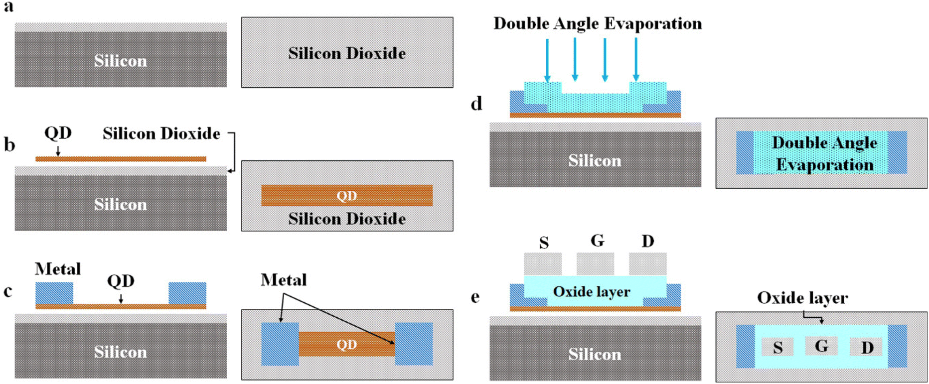 | ||
| Fig. 11 a. Substrate preparation. b. QD transfer using a wet transfer method. c. Metal deposition to define the boundaries of the QD. d. Tunnel barrier formation by the double angle evaporation technique. e. Metallization and a lift-off process. | ||
Reported works indicate that EBL is an effective lithography tool for SET fabrication (Table 4). Because EBL offers unparalleled resolution, it enables the creation of extremely small and precise patterns that are essential for defining the nanoscale features of SETs.128 Due to the presence of a focused electron beam deflector, control over the electron beam's direction is possible. Therefore a mask is not necessary when writing a pattern on a resist. Due to its feasibility, EBL is a very versatile technique that is frequently employed in SET fabrication.129 The required design can be patterned on a resist down to about 30 nm in size with the help of an advanced microscope.
| Method | E-beam energy/wavelength | Beam diameter | Oxide layer thickness | Resist (thickness) | Electrode | Island | Tunnel junction formation | Operating temp. |
|---|---|---|---|---|---|---|---|---|
| EBL56 (1997) | 40 keV | <20 nm | — | MAA (450 nm) | Al | Al | Double angle evaporation | 43 mK |
| PMMA (50 nm) | ||||||||
| EBL130 (2004) | 40 keV | 20 nm | 200 nm | NEB22A (90![[thin space (1/6-em)]](https://www.rsc.org/images/entities/char_2009.gif) 100110 nm) 100110 nm) |
Al | Polysilicon/20 nm | — | 4 K |
| EBL60 (2015) | — | — | 400 nm | PMMA | — | Si/50 nm | Thermal oxidation | 70 K |
| EBL131 (2007) | 100 kV | — | 300 nm | PMMA (350k) | Al | Al/10 nm | RIE | 2 K |
| PMMA (100k) | ||||||||
| EBL132 (2009) | — | — | 200 nm | PMMA | Titanium (40 nm) | SWCNT | O2 plasma etching | 1.5 K |
| EBL60 (2004) | — | — | — | — | Au | Au/10 nm | Electromigration + e-beam evaporation | 4.2 K |
| EBL133 (2016) | — | 4 nm | 300 nm | MMA (450 nm) | Ti (10 nm) | Graphene nanoribbon | O2 + RIE | 4.2 K |
| PMMA (150 nm) | Al (70 nm) | |||||||
| EBL134 (1994) | 30 kV | — | 200 nm | PMMA 70 nm | Al | Al | Two-angle shadow evaporation | 4.2 K |
| MAA 200 nm |
Charge sensors
The fabricated single electron transistors can be used for charge sensing applications by bringing a charge source close to the SET. This could be another quantum dot, a single electron trapped in a potential well or a nearby charge impurity.135 The charge on the source will induce a change in the electrostatic environment of the SET, altering its current. The change in SET current is measured to detect the presence of the charge. This change in potential manifests as a shift in the SET's current–voltage characteristics. By carefully analyzing current variations, one can infer the magnitude and timing of the charge changes.136 The accuracy of the charge sensor can be enhanced using low-noise electronics, such as a low-noise amplifier, which amplifies and measures the tiny current changes in the SET. These can help to improve the signal-to-noise ratio by modulating the SET's gate voltage and demodulating the current signal.Nanoscale characterization techniques
Characterization is the process of evaluating the performance and functionality of a device. Since the SET depends on the behaviour of a single electron, further techniques are needed to estimate these characteristics. The role of characterization in achieving optimal performance in quantum devices, with specific reference to SETs. The foremost characterization method includes electrical transport measurements such as I–V characteristics and gate dependence. The current (I) across the source and drain electrodes is measured in response to the applied voltage (V) using the SET. The energy required to add or remove an electron from the QD inhibits the passage of current, resulting in Coulomb blockade diamonds, which are produced by the current measurement. Additionally, by adjusting the gate voltage, the conductance of the SET may be seen. This indicates how sensitive the apparatus is to variations in the QD's electron count. Then a spectroscopic approach can be used to characterize the SET. In this method, a low-frequency AC voltage is used with the DC bias voltage. Current measurements provide useful information for researchers such as the capacitance of the tunnel junction and the charging energy of the QD. Utilizing noise spectroscopy to measure variations in the current passing through the SET is an additional technique for characterization. By analysing the fluctuations, researchers can determine the discreteness of the charge carriers. This measurement helps to acknowledge the single-electron nature of the device's operation. Then the research community uses electron microscopy as a better characterization technique. A high-resolution image of the SET device is recorded by using imaging techniques such as transmission electron microscopy (TEM) and cryo-electron microscopy (Cryo-EM). This information is used to verify the device's geometry and identify any fabrication defects. Advanced characterization methods like radio-frequency (RF) and low-temperature measurements are also discussed in this article. By incorporating the SET into an RF circuit, researchers can explore its high-frequency characteristics and potential for applications in radio frequency electronics. Since thermal fluctuations can obscure the quantum effects in SETs, characterization often happens at cryogenic temperatures (near absolute zero).Transmission electron microscopy (TEM). TEM is an excellent tool for high-resolution imaging, providing atomic-level detail on the SET's physical structure. After fabrication, TEM allows researchers to validate the actual dimensions of the QD tunnel junctions and electrodes in the SET. These dimensions are critical factors influencing the electrical behaviour. Deviations from the intended design can be identified and potentially addressed for future iterations. Imperfections like irregularities in the QD shape or tunnel junctions can significantly impact the SET's performance. TEM's high magnification allows for the visualization of such defects, aiding in optimizing fabrication processes to minimize them (Fig. 12a left). TEM can be used for compositional analysis to identify the materials used in the SET and any impurities. Understanding the material's properties is crucial for tailoring the device for specific electrical characteristics. For instance, the presence of unwanted dopants might affect the SET's ability to achieve the desired Coulomb blockade effect.
 | ||
| Fig. 12 a. TEM (left) (this figure has been reproduced from ref. 139 with permission from JOVE copyright 2024) and cryo-TEM image of quantum dots (right) (this figure has been reproduced from ref. 140 with permission from European Chemical Societies Publishing copyright 2024). b. I–V (left) and G–V (right) characteristics of a SET (this figure has been reproduced from refs. 31 and 56 with permission from AIP Publishing copyright 2024). c. Noise spectra of a SET (left) (this figure has been reproduced from ref. 141 with permission from AIP Publishing copyright 2024) and power spectral density of the SET (right) (this figure has been reproduced from ref. 142 with permission from Springer Nature copyright 2024). | ||
By providing high-resolution structural information, TEM complements the insights gained from electrical characterization techniques. Observed electrical behaviour in the SET can be linked to specific structural features visualized using TEM. This makes it possible to comprehend the device's atomic-level operation on a deeper level.137 Also identifying structural issues through TEM can guide the refinement of fabrication processes to create more consistent and higher-performing SETs. Future developments in the fascinating subject of nanoelectronics can be facilitated by utilizing the insights obtained from TEM research to optimize the design and manufacture of SETs. TEM's structural insights are helpful for enhancing the functionality and design of these innovative gadgets.138
Cryo-transmission electron microscopy (cryo-TEM). Cryo-TEM is an effective material characterization tool for analysing the morphology of the electrodes and gate structure and the presence of defects or imperfections at the nanoscale level. In contrast to conventional TEM, which runs at room temperature, cryo-TEM subjects the sample to an environment close to the temperature of liquid nitrogen, which is approximately −170 °C or 103 K.143 The sample is flash-frozen at this extremely low temperature in a vitrified (glassy) form, maintaining the nanoparticles’ natural structure and reducing artifacts from chemical fixation or dehydration processes that are employed in traditional approaches.144 Cryo-TEM, pushing the limits of resolution, makes it possible to see individual atoms inside the QD structure. Because of this feasibility, the presence of dopant atoms in the QD lattice can be identified and also any imperfections or defects can be detected that can affect QD performance.145 Cryo-TEM provides information about the elemental composition and electronic structure of the QD. Also the spatial distribution of different elements within the QD can be determined and this can reveal the presence of any unwanted elements or contaminants within the QD.146 One of the important properties related to quantum confinement is the bandgap energy of the material, which can also be analysed. The quantum confinement effect of a 2D material lies within its tuneable layers. The number of layers can be effectively viewed in cryo-TEM analysis (Fig. 12a right).140 The above-discussed information is essential for understanding the fundamental properties of QDs and paving the way for advancements in QD-based technologies.61
Cryogenic probe station. An essential tool for precise electrical characterization of SETs is a cryogenic probe station.147 At room temperature, thermal noise can mask the subtle effects arising from single-electron tunneling in SETs.148 By lowering the temperature using a cryogenic probe station (typically reaching temperatures below 4 K), thermal noise is significantly suppressed, allowing for a clearer observation of the device's single-electron behaviour. The Coulomb blockade effect is strengthened by decreased thermal noise. Thermal noise-induced energy variations are suppressed at cryogenic temperatures in comparison with the SET QD's charging energy. Consequently sharper current peaks are seen in the I–V characteristics, providing a better picture of single-electron tunneling events. This is how the device is configured. The probe station provides a platform to precisely position sharp metallic probes onto the delicate electrodes of the fabricated SET on a semiconductor wafer. These probes make electrical contact with the source, drain and gate electrodes of the SET, enabling the application of voltages and the monitoring of currents. The cryostat within the probe station cools the sample stage, reaching cryogenic temperatures. Thermal insulation and specialized transfer lines ensure the cold environment is maintained around the device.149 Special low-noise cables and amplifiers are often used within the cryogenic environment to minimize noise introduced during measurements due to cable resistances and thermal fluctuations.
Similar to room temperature characterization, current–voltage (I–V) sweeps are performed. The cryogenic environment allows for more precise observation of the current peaks corresponding to single-electron tunneling events. Techniques like capacitance–voltage (C–V) sweeps and four-probe methods can be employed to measure the gate capacitance (Cg) and tunnel junction resistances (Rt) at cryogenic temperatures. These parameters are crucial for understanding the device's behaviour and can be compared to theoretical models. By minimizing thermal noise, cryogenic characterization provides a more accurate picture of the SET's single-electron transport properties. This allows researchers to determine key parameters with greater precision. Understanding the behaviour of SETs at cryogenic temperatures is crucial for optimizing their performance for applications like quantum computing where low-noise operation is essential (Fig. 12b). The data provided show the electrical characteristics of a single-electron transistor (SET) at ultra-low temperatures. On the left, “I–V characteristics at 43 mK” depict current versus voltage, revealing conductivity changes. On the right, “G–V characteristics at 60 mK” show conductance versus gate voltage, illustrating gate modulation. Both measurements, taken at millikelvin temperatures, demonstrate the SET's quantum behavior, specifically the Coulomb blockade essential for single-electron control. Cryogenic probe stations are a vital tool for researchers studying and developing SETs. By enabling characterization at ultra-low temperatures, they provide valuable insights into the single-electron transport mechanisms within these devices, paving the way for advancements in nanoelectronics and quantum technologies.150
Noise spectroscopy uses lock-in amplifiers and a spectrum analyser. The lock-in amplifiers provide a selective measurement of the noise power at a specific frequency of interest by rejecting background noise. By sweeping the lock-in frequency, researchers can obtain the complete noise spectrum of the SET.152 A spectrum analyser can display the entire noise spectrum over a wide frequency range, providing a broader picture of the noise behaviour in the SET. By identifying and mitigating dominant noise sources, researchers can create SETs with better sensitivity and lower noise levels. Noise spectroscopy provides useful information about the fundamental physical processes occurring within the SET, which helps to better understand how the SET functions. Reduced noise levels in SETs are crucial for their application in areas like quantum computing where high sensitivity is essential for reliable operation for gas sensing applications.
Careful design of the charge sensor itself can minimize internal noise sources. Techniques like proper grounding and shielding can help reduce environmental noise. The signal intensity in relation to noise can be increased by applying filtering and amplification techniques. However these techniques need to be carefully implemented to avoid distorting the signal itself. In some cases, operating the sensor at lower temperatures can help reduce thermal noise. Additionally shielding the sensor from external noise sources can significantly improve the SNR. By understanding and optimizing SNRs, researchers and engineers can ensure that their charge sensing systems deliver accurate and reliable measurements, paving the way for advancements in various scientific and technological fields.155 SETs and their electrical, material and noise characteristics have been investigated (Table 5).31,37,56,71,73,141,156–187

|

|

|

|
Applications of SETs for charge sensing
SETs are a perfect match for QD sensing due to their complementary characteristics. QDs are tiny semiconductor structures that can trap a specific number of electrons. Their properties are highly sensitive to the number of trapped charges. SETs are excellent at reading the occupancy of a QD because of their extraordinary capacity to detect minuscule changes in charge (down to a fraction of an electron). Researchers can accurately count the electrons in the dot by observing the current flowing through the SET. Due to their ability to store quantum information contained in the spin or charge state of trapped electrons, QDs show potential for use in quantum computing applications.188 SETs function as highly sensitive probes that can “read out” these quantum states by detecting the subtle changes in charge associated with different spin or occupancy configurations. Researchers might adjust the energy levels of the QD by varying voltage pulses applied to the SET's gate electrode. They can thus investigate the energy spectrum of the dot and gain an understanding of its interactions with its surroundings and electrical structure. Crucially important for quantum information processing, SETs are employed in quantum computers to read out the state of the QD qubit. All things considered, SETs provide researchers exploring the interesting realm of QDs with a priceless instrument. Because of their unmatched sensitivity to charge, which allows new directions for quantum computing spintronics and other cutting-edge sciences, these nanostructures can be exactly defined.189Biomolecule detection
SET-based single-molecule biosensors offer a potent means of identifying the presence and activity of individual biomolecules. With great sensitivity, this method lets researchers examine occurrences at the single-molecule level. Many times, when analysing bulk samples, traditional biosensors produce an average response. Biological processes however can show notable variability whereby individual molecules behave differently. By spotting and evaluating the activity of every molecule, single-molecule biosensors can get beyond this restriction and offer a better understanding of biological events.190 Nevertheless, a significant obstacle facing modern biosensors is achieving real-time single-molecule resolution for in situ activity detection in natural materials. The label-free real-time detection of biological molecules, including viruses, proteins and nucleic acids, is made possible by single-molecule electronic biosensors, which have high sensitivity and specificity.191 The outline of the operation of single-molecule electrical biosensors is given in this section.The working mechanism of biomolecule detection is based on finding the variation in the electrical conductance using SETs.192 The surface of the SET needs to be modified to selectively bind with the target biomolecule. This is achieved by attaching a receptor molecule to the SET surface. The receptor molecule may be a protein, DNA, RNA (ribonucleic acid) and other biorecognition molecules. The target biomolecule modifies the electrical characteristics of the SET and influences the current flow when it binds to the receptor on the SET surface.23 By enabling the target molecular electrostatic potential to electrostatically alter the electron fluxes of the conductive channel, a single molecule SET biosensor may detect signals. The target molecules’ interactions can be swiftly translated into readable electrical signals in real-time by the molecularly gated sensing method.193 This change in current is measured and analysed to detect the presence and potentially the concentration of the target biomolecule. By employing signal processing techniques, it is feasible to improve detection accuracy and the signal-to-noise ratio.27
A recent cutting-edge study suggests that in order to improve the effectiveness of biomolecule detectors, the size of the sensing channel's nanomaterials should be similar to that of the majority of biological entities, including viruses, proteins and so on. Thus silicon nanowires (SiNWs),22 single wall carbon nanotubes (SWCNTs)194 and 2D materials (graphene, transition metal dichalcogenides)195 can be used as a biosensor. Because of their complementary size scale, changes in a trapped molecule can immediately alter the carrier density at the tiny nanometric sensing channel surface.22 When a single biomolecule interacts with the conductive channel, the field effect or dispersion effect, like a switch valve, causes the modification of the sensor site to substantially modify the conductivity of the entire device. Consequently the electrical nano-biosensors have sufficient sensitivity to distinguish specific proteins. The devices’ electrical impulses make it possible to directly identify and track the dynamic actions of individual molecules. In order to connect with other target molecules in the solution, the single molecule that is attached can also be used as a probe. This probe–target interaction technique enables single-molecule resolution to identify target molecules over a broad concentration range (millimicrons).196 Target biomolecule concentrations are provided and summarized for single-molecule detection employing representative electronic biosensors (Table 6).
Because single-molecule detection technology is developing so quickly, the integration of electrical and optical detection of single molecules has proved to be beneficial for the research of single-molecule biodynamics, especially the single molecular junction.
Scanning microscopy
Owing to its submicron spatial resolution in detecting static electric fields, SETs can be employed as scanning probe microscopes. In addition to that, scanning SET microscopy uses the characteristics of sensing charges with fractional electron charge sensitivity of 0.01e. There is a specialized technique called scanning SET microscopy (SETSM) that utilizes a SET as a probe. Here, the SET is mounted on a tip and scanned very close to the sample surface.197 The SET's capacity to detect the electric field from the sample allows researchers to map static electric fields and charges with remarkably high sensitivity down to a fraction of an electron charge. This provides information complementary to that of SEM, offering insights into the electrical properties of the sample at the nanoscale. Building a scanning SET microscopy (SETSM) involves crafting a tiny transistor on a sharp tip and then integrating it with supercooled electronics and a precise scanner. This delicate dance requires advanced fabrication techniques to create the transistor followed by meticulous mounting onto a probe tip. Electrical connections are established and the whole setup is chilled to near absolute zero for optimal performance. Finally, a computer-controlled scanner meticulously moves the tip across the sample, capturing the electrical landscape with unmatched sensitivity (Fig. 13a). | ||
| Fig. 13 a. Schematic representation of a SET with a probe tip located above the 2DEG heterostructure. An enhanced picture of the tip and an example of a cutaway (inset) (this figure has been reproduced from ref. 200 with permission from Elsevier copyright 2024). b. Spin-based tunneling mechanism (left) and the readout mechanism (right) (this figure has been reproduced from ref. 59 with permission from Springer Nature copyright 2024). | ||
With the ability to detect electron charge fractions as small as −1% of an electron, SETSM exhibits exceptional sensitivity. This surpasses other scanning probe microscopy techniques in electrical field detection. While not quite reaching atomic resolution, SETSM offers excellent spatial resolution of around 100 nm, allowing for detailed imaging of electrical features on the nanoscale. Scanning SET microscopy consists of various applications, such as the characterization of the electrical properties of semiconductor materials and devices, including dopant profiles, band bending and trapped charges. Investigating the electrical characteristics of several nanomaterials, including graphene and other two-dimensional materials, benefits from the method. Investigating the electrical activity of biomolecules and biological systems is one of the recently developed uses. SETSM needs cryogenic temperatures often below 1 K for the best performance. This restricts its more general usefulness. The fabrication of SET probes can be challenging and requires specialized techniques. SETSM measurements can be slow due to the need for precise positioning and high sensitivity. Despite these limitations, scanning single-electron transistor microscopy is rapidly evolving technology with immense potential for pushing the boundaries of electrical characterization at the nanoscale.198
SETs and probes with greater sensitivity or smaller size will need to be developed in order to further enhance the SETSM. It is possible to enhance the current SETSM's resolution to approximately 10 nm by utilizing smaller fibers and tips, along with somewhat thinner sheets. The operating temperature would rise proportionately with this configuration. Although it is feasible, room temperature operation would necessitate the creation of SET tips that were atomic or molecular in size. This microscopic technique's sensitivity to potential charge capacitance, interface potential, conductance and dielectric materials could be useful for a number of basic and applied challenges.199 For example, SETSM investigations are relevant for the characteristics of electrons in the quantum Hall regime and their edge states. By applying single-electron capacitance spectroscopy, a potent technique for capturing the entire electron energy structure of mesoscopic systems, SETSM may be able to increase its capacity for spatial mapping.
Spin-readout mechanism (spintronics)
The spin readout mechanism can be implemented with a SET. With regard to spintronics, the single-electron charge sensor's readout process is based on one electron's spin. The weak spin–orbit from the bulk crystal in silicon allows for an electron spin to represent an independent quantum bit with lengthy coherence durations. Therefore, it is extremely difficult, if not impossible, to observe and manipulate a single electron to observe and manipulate an atom's single spin.201 According to recent studies, a single-shot method can be used to read out an electron spin in silicon. This is made possible by implanting phosphorus donors alongside a metal oxide semiconductor SET. The spin readout was usually obtained by spin-dependent tunneling where the electron was shifted to a different location according to its spin. The charge detector, which sensed whether the charge had shifted, was electrostatically coupled to the electron site and determined the spin state. Charge sensing has been accomplished by both tunnel coupling to the electron location and electrostatically coupling the detector (Fig. 13b left).59 An “electron site” is a designated area within the device where an electron might be confined. This could be a real physical location, such as a defect or a QD, whereby the electron's energy is reduced, therefore trapping it in the surrounding area. By tracking the characteristics of this location and deducing information regarding the presence or absence of a single electron, researchers can accomplish single-electron charge sensing. In the end, the robust coupling configuration will enable high fidelity and a speedy spin readout. A charge sensor or detector is one used for a SET. A characteristic pattern of sharp current peaks as a function of gate voltage results from the QD's electrochemical potential having to take particular values before a current may flow from source to drain. A single electron tunneling into the SET QD from a nearby charge centre causes an electrochemical potential change that allows the current to be switched from zero to its maximum value. This tunneling event becomes spin-dependent when a strong external magnetic field B is present. The energy difference between the spin-up |↑〉 and spin-down |↓〉 states represented by EZ = gμBB, with g ≈ 2 as the spin gyromagnetic ratio and μB as the Bohr magneton, is due to the spin-up state's higher energy. The thermal and electromagnetic spreading of energy states in the SET QD must be greater than the Zeeman splitting, EZ. Thus, in order to perceive the sensing effect, a high magnetic field, B > 1 T, and a very low electron temperature, Tel ≈ 200 mK, should be maintained.202A phosphorus atom intrinsically gives its bound donor electron a strong confinement potential in silicon. Like phosphorus, in silicon donor atoms bring extra energy states to the SET channel. As already noted, these states can function as isolated “electron sites”.201 Donor atoms offer a varied and well-defined electron location. This makes the behavior of the SET more predictable and under control than depending on possible fluctuations or channel-owning flaws. The additional energy level introduced by the donor can improve the stability of the single-electron QD, reducing thermal noise and unwanted charge fluctuations.203 As a result, a set of devices was created and P donors were inserted into a tiny area adjacent to the SET. Three donors are located between 30 and 60 nm away from the SET QD. These donor atoms are tunnel-coupled to the SET QD to achieve a parallel double-quantum dot system. To perform spin readout, the gates of the SET were biased. Then the electrochemical potentials on the SET (μSET) and a nearby donor were tuned such that the SET current, ISET, was zero when the electron resided on the donor while ISET ≠ 0 when the donor was ionized.
The gates of the SET are biased in order to achieve spin readout. The electrochemical potentials of the SET (μSET) and a nearby donor were then adjusted so that, in the absence of an electron on the donor, the SET current, ISET, was zero. In the presence of an electron on the donor, ISET is not zero. There are three phases of the readout mechanism (Fig. 13b right). (1) A load phase is defined as follows: μSET > μ↑μ↓, where an electron from an unknown spin state can tunnel from the donor to the SET QD. ISET decreasing to zero indicates electron loading. (2) A read phase where ISET = 0 is caused by a spin-down electron that is trapped onto the donor; nevertheless, ISET = Imax can be caused by a spin-up electron that tunnels onto the SET QD. Later the other spin-down electron from the SET QD returns to the donor through a tunnel once more obstructing the current. As a result, at the start of the read phase, the signal's spin state |↑〉 is just one current pulse. (3) To guarantee that an extra electron with a random orientation can be loaded at the next cycle, the donor is ionized during an “empty” phase.204
Memory devices
There is still more research to be done on the SET and its potential as a memory device. SETs exploit the principle of the Coulomb blockade. This effect essentially restricts the flow of current through a narrow channel (QD) due to the repulsion between electrons. By applying a voltage to a gate electrode on the SET, researchers can modify the number of electrons in the QD. An electron's existence or absence can correspond to a binary state (1 or 0) in a memory unit.205 Due to their small size, SETs offer the potential for very high-density memory compared to conventional transistors. On a chip, the tiny components involved in a SET can be packed far more densely than on conventional transistors. The storage capacity per unit area therefore rises dramatically as a result. By adding or subtracting electrons from the quantum dot, one can create information that can be read by either the presence or absence of electrons. SETs are perfect for low-power memory uses since their running operation requires little current flow. SETs are inherently resistant to radiation damage, a significant concern for memory units in space electronics.206 The QD's electron count can be difficult to regulate accurately, which increases the risk of read/write errors in the memory unit.207 Researchers are striving to overcome these obstacles right now. Here are some key focus areas: Developing new materials aims to create SETs that operate at higher temperatures. Also, advancements in nanofabrication aim to simplify and reduce the cost of SET production. Methods under investigation are meant to reduce read/write mistakes and guarantee data integrity. SET memory is a promising path for future memory technology, even if the discussed restrictions prevent it from being widely adopted now. Based on SETs, ongoing research might produce low-power, high-density, radiation-resistant memory devices.Matsumoto et al. employed an MTJ (multiple tunnel junction) memory in GaAs operating at 4.2 K to develop the first single-electron memory cell ever purposefully made.208 Using an atomic force microscope, Nakazato et al. created a room temperature MTJ single-electron memory. To precisely control a finite quantity of electrons stored on a memory node, Nakazato et al. developed a substitute apparatus comprised of a silicon-on-insulator (SOI) multiple tunnel junction (Fig. 14a). Another important aspect of single-electron memory is the need for a very sensitive SET electrometer current to identify the minute charges of stored electrons.209
 | ||
| Fig. 14 a. Schematic circuit diagram of a single-electron memory cell. b. Circuit diagram of a SET (left). Circuit implementation of a SET using MOSFET (right). | ||
Due to their minuscule size and low power consumption, single-electronic transistors or SETs are a promising component for the next generation of transistors. More researchers are focusing on N-dimensional multi-QD SETs since single-QD SETs cannot function well at high temperatures. The cited article presents a novel design for single-electron memory.210 For memory operation, SETs and a two-dimensional regular array of multiple tunnel junctions (MTJs) on a nanowire make the perfect combination. Thermionic and Coulomb blockade effects play important roles in the system's carrier conduction at ambient temperature. The charge of the memory node is found with a nanowire MTJ electrometer. A properly defined parameter lets individual electrons in tunnel junction circuits be charged at ambient temperature.211 By sufficiently restricting and regulating electron behavior, quantum dots present a viable path for creating high-density memory systems. Faster read and write speeds and better data retention follow from this compared with conventional memory technology.
Operating conditions
SETs exhibit optimal performance at low operating temperatures and hence often require cryogenic conditions (extremely low temperatures). A key principle behind SET operation is precise control over single electrons.212 The energy levels of the SET's conducting channel determine this control since the gate voltage allows for changing of these levels. The irregular thermal mobility of electrons inside the device causes thermal noise, which disturbs this control. Thermal noise becomes more important at higher temperatures, which makes it challenging to separate the random fluctuations resulting from thermal effects from the single-electron energy levels. By lowering the operating temperature, researchers can significantly reduce thermal noise in SETs.213 This allows for clearer distinctions between the discrete energy levels and enables more precise control over single electrons using the gate voltage. A low temperature environment also helps to reduce the leakage current in SETs. Leakage currents, where unintended current flows through undesirable paths, can be a challenge in SETs. Lower temperatures can help minimize these leakage currents, leading to more accurate control over single-electron transport.214 Also, a low temperature environment improves the subthreshold swing. The subthreshold swing measures the gate voltage's ability to control the current passing through the SET. Lower temperatures can lead to a steeper subthreshold swing, indicating a sharper transition between the ON and OFF states of the SET.There are several techniques used to achieve cryogenic temperatures for SETs. One way to implement a low-temperature environment is dilution refrigeration. The temperature can be lowered to a few millikelvin (thousandths of a Kelvin) with this extremely effective method. It utilizes a mixture of two isotopes of helium (He-3 and He-4) to achieve cooling through a complex process involving pressure changes and phase transitions. Dilution refrigerators are expensive, complex to operate and require a pre-cooling stage with liquid helium. The helium-3 refrigeration method uses liquid He-3 to achieve temperatures in the range of 0.3 K.215 It is simpler to operate than dilution refrigerators but still requires a pre-cooling stage with liquid nitrogen and liquid helium. A liquid helium bath, involving immersing the SET device in a bath of liquid helium (boiling point around 4.2 K), is a relatively simple and cost-effective approach.216 However it does not reach the ultra-low temperatures achievable with other methods. Stirling cycle cryocoolers utilize the Stirling cycle, a closed regenerative thermodynamic cycle, to achieve cryogenic temperatures (around 50 K) using electrical power. They offer a more compact and portable solution compared to liquid-based cooling but may not reach the extremely low temperatures needed for some SET applications.217
However the requirement for low-temperature environments in SETs poses several limitations for practical applications in certain environments, making them less suitable for real-world use in many cases. Implementing and maintaining cryogenic cooling systems is complex and expensive. This includes the cost of the cooling equipment itself, the infrastructure needed to operate it (e.g. liquid helium supplies, vacuum pumps) and the expertise required for system maintenance. These factors make SETs less attractive for cost-sensitive applications. Cryogenic systems are often bulky and energy-intensive. This makes it challenging to integrate a large number of SETs into a single device or system, limiting their scalability for applications requiring high-density circuits. Cryogenic cooling systems are not portable due to their size and complexity. This makes SETs impractical for applications requiring mobile devices or operations in remote locations with limited access to cryogenic infrastructure. Maintaining extremely low temperatures can be difficult or even impossible in certain environments such as those with high ambient temperatures or limited power availability. This restricts the use of SETs in these scenarios. SETs are appealing candidates for application in the development of quantum computing because they have the ability to control individual electrons. However the cryogenic requirement makes large-scale quantum computers using SETs challenging to achieve. SETs’ compact size and single-electron control make them potentially capable of providing ultra-dense memory. However the complexity and cost of cryogenic cooling make them less competitive with existing memory technologies for most consumer applications. SETs have the potential for being highly sensitive sensors due to their precise control over single electrons. Their applicability in portable or remote sensing projects is limited nonetheless by the cryogenic requirement.
Challenges and limitations of SETs for charge sensing
Issues due to noise
SETs are well-known for their incredible sensitivity in spotting minute changes in charge. Still, diverse noise sources impede their strive for absolute precision therefore influencing their performance. Various types of noise can influence SETs; each one influences the functioning of the device in a different manner. Electronic noise in the form of burst noise or random telegraph noise (RTN) is present in ultra-thin gate oxide layers and semiconductors. Generally the sub-micrometre device will be subjected to the impact of RTS noise on its operation. Specifically for SETs, as nanoscopic devices, RTN noise may be the major obstacle to their operation. It is caused by a single electron trapping and de-trapping in a defect state, which can lead to undesirable current fluctuations. The fluctuations are caused by switching events that depend on capture and emission events of individual electrons by traps in the gate oxide. Both the channel charge and the channel mobility are impacted by changes in a trap's charge. The oscillations in universal conductance are another source of RTN noise in mesoscopic systems.158 One characteristic that distinguishes RTN is abrupt step-like transitions between two or more voltage or current levels at random and unpredictable periods. Each offset voltage or current shift may last anywhere from a few milliseconds to many seconds. Thermal fluctuations of the SET might arbitrarily trap and release charge carriers. This takes place at fault sites or transistor interfaces. The random trapping and release of charges cause the current measured by the SET to vary. RTN causes undesired noise in the SET's signal therefore compromising the accuracy of the ultrasensitive charge detecting capacity. Then thermal noise is produced due to thermal vibrations of atoms, which can create noise in the SET. This may cause very small changes in the current passing through the apparatus, which would compromise the measurement precision of the charge. Additionally, the statistical character of electron flow is the source of shot noise.141 When electrons tunnel through tunnel barriers, they produce that shot noise. Typically, a two-junction configuration without a gate produces shot noise. Even in a constant current, electrons do not arrive perfectly uniformly, leading to slight random fluctuations. This phenomenon resembles water dripping from a leaky faucet – there will be occasional spurts and drips, not a perfectly smooth flow. Finally, flicker type noise has a specific frequency dependence and can mask the desired signal from the SET. It characterizes noise in which the inverse relationship between frequency and power spectral density leads to a 1/f dependence. This indicates that as the frequency increases, the noise level progressively decreases from a higher level at lower frequencies. Flicker noise appears when the SET frequency drops below 1 kHz. It is common to observe deviations from a 1/f spectrum typically in conjunction with telegraph noise. Variations from a 1/f spectrum are frequently observed, usually in combination with telegraph noise. Flicker noise occurs when electrons make random transitions at a single trap.218 A single trap can introduce significant noise into a SET, limiting its accuracy and performance at the single-electron level. A trap is a flaw or imperfection in the SET's conducting channel or insulating layer. Like little capacitors, these traps can capture or release electrons. When an electron is trapped or released from a trap, the local charge distribution inside the SET changes suddenly. This charge change could throw off the fragile single-electron transport equilibrium.One important metric that aids in comprehending how noise impacts the sensitivity of SETs is the signal-to-noise ratio (SNR). The signal-to-noise ratio or SNR is defined as the signal volume divided by the noise level. A low SNR makes it challenging to discern the signal from the noise, whereas a high SNR indicates that the signal is distinct and easy to see. High noise levels cause the faint signal from the small charge shift to be buried. The SET thus battles to separate the real signal from noise-induced random variations. High noise levels essentially lower a SET's sensitivity since it depends on identifying these little changes in charge. To be seen over the noise, a higher signal is needed; hence the range of charge changes the SET can consistently detect is limited.
A theoretical modeling of the Debye–Lorentzian distribution can help reduce flicker noise. The 1/f noise behaviour in SETs is simulated using a mathematical function known as the Debye–Lorentzian distribution. The Debye function captures the low-frequency feature of the noise, which is a gradual reduction in noise power density with increasing frequency. The Lorentzian function represents the noise's high-frequency behaviour, where the noise power density falls off more quickly at higher frequencies.219 Researchers can determine the primary noise sources in their SET devices by applying the Debye–Lorentzian distribution to analyse the 1/f noise spectrum. And one can develop strategies to minimize 1/f noise and improve the performance and reliability of SETs. A SET can only allow consecutive electron transmission because of the Coulomb barrier. For symmetric tunnel couplings, this results in a minimal Fano factor of FSET = S/SP = 0.5. Therefore, shot noise measurements provide a profound understanding of the underlying physical mechanisms of a system. More time correlations between the tunneling events are needed in single-electron devices in order to further reduce shot noise. One method is to use turnstiles and single-electron pumps to drive the tunneling process on a periodic basis, catching and releasing one electron every cycle. However, the random fluctuations of the underlying quantum mechanical tunneling process are not well-absorbed by these open-loop devices, which inevitably causes shot noise to rise.220
Given noise is the main issue impeding SETs’ ultimate sensitivity, researchers have developed several approaches to address it. Using materials with fewer flaws and higher purity will help reduce charge-trapping sites that support RTN. Optimizing the SET's geometry such as channel size and gate control will reduce noise sensitivity.221 Precise control during fabrication ensures consistent device characteristics and minimizes unwanted variations that can introduce noise. Cooling the SET to cryogenic temperatures significantly reduces thermal noise, improving the SNR. However this approach has limitations for practical applications. Applying specific voltage pulses to the SET's gate can help average out some noise sources like RTN, leading to a more stable signal (gating technique). Using filters designed for specific noise frequencies can help remove unwanted components from the SET's output signal.222 Designing low-noise readout electronics minimizes additional noise introduced during signal processing and amplification. Carbon nanotube SETs offer the potential for reduced RTN due to their unique properties. Double-QD SET design can improve noise immunity compared to traditional SETs.173
Integration challenges
Integrating SETs with other electronic components for complex sensing systems presents several challenges. SETs often require specialized materials with unique properties different from those used in conventional electronics. This can make it difficult to integrate them seamlessly with standard CMOS (complementary metal–oxide–semiconductor) processes used for most electronic components. Creating reliable and low-resistance electrical connections between SETs and other components can be difficult. Interface problems can lead to unwanted noise and degraded performance.223 Most SETs, as already stated, currently need cryogenic temperatures to function best. The integration of them with other components that usually run at room temperature is a major difficulty. Designing and running a system including room-temperature and cryogenic components increases complexity. The weak signal from a single electron in a SET needs to be amplified and converted into a usable signal for further processing. Designing and integrating low-noise, high-fidelity readout electronics specifically for SETs can be a challenge. SETs are highly sensitive to noise, which can disrupt their operation. Integrating them with noisy components or operating them in noisy environments can significantly impact their performance and reliability.224The 3D integration and heterogeneous packaging are novel integration techniques that offer advantages over traditional planar integration methods for electronic devices. The 3D integration technique involves stacking multiple layers of integrated circuits (ICs) vertically on top of each other, creating a three-dimensional circuit structure. Interconnections between layers are made through holes etched through the layers and microbumps (tiny solder joints). 3D stacking allows for more components to be integrated within a smaller footprint, which is crucial for the miniaturization of complex sensing systems.225 By placing components closer together vertically, 3D integration reduces interconnection lengths between SETs and other components. This minimizes signal delays and improves overall system performance. Heterogeneous integration allows for the stacking of different types of ICs including SETs fabricated on specialized materials with conventional CMOS components on separate layers. This enables the integration of SETs with other electronic components despite potential material mismatches.226
The heterogeneous integration approach focuses on packaging pre-fabricated ICs or individual electronic components together using advanced packaging techniques.227 Unlike 3D integration, the components are not necessarily stacked vertically but can be arranged in a more flexible way within the package. Heterogeneous packaging allows for a modular approach where SETs fabricated on their optimal materials can be integrated with pre-fabricated CMOS readout electronics or other components in a single package. This simplifies the overall fabrication complexity. Developments in high-density low-parasitic interconnects, miniaturized packaging materials and advanced thermal management solutions will improve the capabilities of heterogeneous packaging for integrating SETs with different components. This offers more flexibility in terms of component placement and routing compared to 3D stacking.228
Beyond 3D integration and heterogeneous packaging, there are a few other emerging techniques being explored for integrating SETs with other electronic components. The nanowire integration technique utilizes nanowires, which are extremely thin semiconductor wires, to fabricate SETs and interconnect them with other components. Nanowires can be made from various materials, including silicon gallium nitride or carbon nanotubes. Nanowires can be grown and patterned with high precision, allowing for flexible integration with other components on a variety of substrates.229 However forming reliable and low-resistance electrical connections between nanowire SETs and other components can be challenging due to their small size. Another technique is transfer printing. This technique involves fabricating SETs on a sacrificial substrate and then transferring them onto another substrate where they are integrated with other electronic components. This makes it possible to optimize the SET fabrication process and system integration as a whole independently. Another solution is the integration of SET with the CMOS technique.230 This approach aims to develop fabrication processes that allow for the simultaneous fabrication of SETs and conventional CMOS (complementary metal–oxide–semiconductor) components on the same chip. This would significantly simplify integration and potentially reduce overall system costs.
While integrating quantum mechanics devices with conventional electronic devices, one of the major issues is combining low-temperature devices with room temperature control unit/readout circuits. Thus integrating low-temperature SETs with room-temperature devices presents several significant challenges that hinder the development of practical SET-based systems. SETs typically operate at cryogenic temperatures (around 4 K or −269 °C) to minimize thermal noise. However, most electronic components are designed to function at room temperature (around 300 K or 27 °C). This vast temperature difference leads to a significant thermal expansion mismatch between the materials used in SETs and room-temperature devices. As the temperature changes, the materials in the system expand or contract at different rates. This may result in physical harm as well as tension and strain where the SET interacts with other components, which could impair the SET's functionality. SETs are highly sensitive to noise. Readout electronics operating at room temperature might introduce additional noise that could disrupt the weak signal from the SET, requiring specialized low-noise designs for reliable signal processing. The characteristics of readout electronics can change with temperature. This can lead to calibration and performance issues when interfacing with a cryogenic SET.
One remaining major challenge is interfacing low-temperature SETs with room-temperature electronics. Ongoing materials science thermal management integration and room-temperature SET development research promises to overcome these obstacles nevertheless. The development of advanced materials with minimal thermal expansion coefficient mismatch between the SET and other components could reduce stress and strain issues. In addition to that, techniques like 3D integration or heterogeneous packaging could potentially minimize the physical separation between the SET and other components, reducing thermal gradients and signal degradation. Similarly, developing low-noise high-fidelity readout electronics specifically designed for interfacing with cryogenic SETs is crucial for reliable signal processing. If not, the most significant remedy would be creating SETs with room temperature efficiency. This would simplify integration with other components and remove the need for intricate cooling systems.
To develop more integrable SET based sensors, recent research work has moved to cryo-CMOS implementation.231 An integrated circuit that is specifically made to function at very low temperatures, usually around 4 K (−269 °C), is known as a cryogenic CMOS. Since SETs can regulate single electrons, they have extraordinary sensitivity. But the necessity for cryogenic cooling systems now limits their useful utilization, particularly in sensor development. This limits their portability and increases complexity and cost. For interacting with SETs in sensor systems, a cryogenic CMOS is a possible answer. Cryo-CMOS circuits are specifically designed to function efficiently at very low temperatures similar to the operating environment required for SETs. Cryo-CMOS technology helps to build control and readout circuitry for SETs able to operate in the same cryogenic environment. This simplifies system design and might increase the general performance by removing the requirement for a sophisticated interface between SETs and room-temperature circuits. In SETs, as well as cryo-CMOS circuits, cryogenic temperatures greatly lower thermal noise. This reduces noise interference with the SET's weak signals, thereby producing more dependable and precise sensor data. Cryo-CMOS circuits can be designed to perform signal amplification filtering and data conversion within the cryogenic environment. This reduces the need for additional room-temperature electronics, leading to more compact and integrated sensor systems.232
But cryo-CMOS technology is still under development and commercially available options might be limited. Continuous research aims to raise the performance and manufacturing feasibility of cryo-CMOS circuits. Designing and fabricating cryo-CMOS circuits can be complex and expensive compared to standard CMOS processes. The whole sensor system—including cryo-CMOS components and SETs—must be built to operate within the cryogenic environment. This calls for sensible packing techniques and heat control. Before a cryo-CMOS is extensively applied in SET-based sensor applications however, problems with cost scalability and complexity of system design still have to be addressed. A cryo-CMOS offers a valuable approach for overcoming the limitations of SETs in sensor development by providing control and readout circuitry that can operate efficiently at cryogenic temperatures. While challenges remain, ongoing research holds promise for a cryo-CMOS to become a key enabler for next-generation, highly sensitive and miniaturized SET-based sensors.
Other quantum sensor technologies
 | ||
| Fig. 15 a. Principle of the NV centre for measuring a magnetic field (this figure has been reproduced from ref. 234 with permission from Springer Nature copyright 2024). b. Trapped-ion quantum sensor (this figure has been reproduced from ref. 235 with permission Springer Nature copyright 2024). c. Schematic of quantum capacitance spectroscopy (this figure has been reproduced from ref. 236 with permission from Springer Nature copyright 2024). d. Illustration of a superconducting quantum interference device (SQUID). e. Block diagram of a cesium atomic clock (this figure has been reproduced from ref. 237 with permission from Springer Nature copyright 2024). f. Diagram of an atomic interferometer gravimeter (this figure has been reproduced from ref. 238 with permission from Taylor & Francis copyright 2024). | ||
Generally, NV centres can be made by implanting nitrogen atoms and by an annealing process. Also microwaves are used to manipulate the NV centre's spin state and laser used to read the spin state through fluorescence. The changes in fluorescence intensity can be correlated to the amount of charge present. Techniques like dynamic decoupling can be used to enhance the sensitivity of NV centre charge sensors. By applying specific microwave pulse sequences, the NV centre's spin coherence time can be extended, leading to improved sensitivity.234 However, in the case of the NV centre, the readout mechanism is based on optical signals, which measure changes in fluorescence intensity. Hence, the NV centre requires optical and microwave instrumentation. But the SET readout mechanism relies on electric signals, which are measured in terms of voltage or currents. Thus the SET leads to relatively straightforward electrical signal processing.
In practice, a single ion can be trapped in an electromagnetic field. The first quantum state is initialized using a laser. Then the electric field to be measured is applied to the trapped ion. The lasers are used to probe the trapped ion state and the change in state indicates the presence and strength of the electric field. In the case of a charge sensor, any nearby charge will generate an electric field that influences the trapped ion. The sensor is calibrated by applying known electric fields and measuring the corresponding changes in the ion's state. Thus trapped ions are more stable but require complex optical systems for the read-out mechanism. But SET provides a direct and simple read-out system. However, the coherence time in SETs can be limited by noise and environmental factors.
Initially, a nanoscale device based on a quantum dot, nanowire, or 2D material structure is fabricated with electrodes. Then the applied voltage is provided and the respective capacitance is measured. A voltage is swept across the device and the capacitance is measured as a function of voltage. Changes in the capacitance signal indicate changes in the charge distribution within the device.236 QCS can achieve high sensitivity because it directly probes the quantum nature of charge carriers. QCS can be a non-invasive technique, as it does not require a direct current flow through the device. QCS can provide an overview of the electronic structure, while SETs can provide detailed information about individual charge states and tunneling events.
A SQUID essentially consists of a loop made of superconducting material. This loop is crucial for the device's ability to detect extremely subtle changes in magnetic fields. Within this superconducting loop, there are one or more Josephson junctions. These junctions are weakly coupled to the superconducting circuit created by thin insulating barriers between superconducting materials. The Josephson junctions make the SQUID so sensitive. They allow for the quantum mechanical tunneling of superconducting electrons. When a magnetic field is applied to the SQUID loop, a circulating current is induced within the loop. The Josephson junctions cause interference effects in this current, which are highly sensitive to even the tiniest changes in the magnetic flux passing through the loop. By measuring these interference effects, the strength of the magnetic field can be determined with incredible precision. SQUIDs can be used as sensitive detectors for manipulating and reading out quantum information. SQUIDs are primarily designed to measure magnetic fields, and SETs are primarily for electric charge. Both quantum sensor technologies require a cryogenic operating temperature but they are meant for different purposes.
The time is measured by counting the number of oscillations of these atomic transitions. The transition frequencies of atoms are sensitive to external fields such as a magnetic field, an electric field, the gravitational field and temperature. Because atomic clocks can measure frequency with extremely high precision, they can detect very small changes in these external fields. Atomic clocks and single-electron transistors (SETs) are both highly precise quantum devices, but they operate on vastly different principles and are designed for distinct purposes. Atomic clocks are optimized for precise time and frequency measurements, leveraging the stability of atomic transitions. SETs are optimized for detecting minute changes in electric charge, leveraging the controlled tunneling of single electrons. Atomic clocks are very stable and are used as a standard where SETs are very sensitive to charge changes.
Usually when deploying lasers, atoms are chilled to extremely low temperatures, producing a cloud of cold atoms or possibly a Bose–Einstein condensate (BEC). This is essential to improve an atom's wave character. “Mirrors” and “beam splitters” for the atom waves are laser pulses (Fig. 15f). These laser pulses separate and recombine the momentum states of the atoms through manipulation. The atoms are in a quantum superposition, meaning they exist in several states concurrently and follow several routes simultaneously. As the atoms propagate along their respective paths, they accumulate a phase that depends on the forces and fields they encounter such as gravity, acceleration, rotation and magnetic fields. The atom waves are then recombined and the resulting interference pattern is measured. The interference pattern reveals the phase difference between the waves, which is directly related to the forces or fields that are present. Atom interferometers are extremely sensitive to minute changes in forces and fields due to the high precision with which the phase of atom waves can be measured. Thus atomic interferometers and single-electron transistors (SETs) are optimized for measuring forces related to motion and gravity by utilizing the wave properties of atoms. SETs are optimized for measuring electric charge by utilizing the controlled flow of individual electrons. They are both very sensitive quantum tools that are used in very different applications. Table 7 provides a comparison between different quantum sensor technologies with SETs.
| Technology | Principle | Sensitivity | Primary applications | Operating conditions | Strengths | Limitations |
|---|---|---|---|---|---|---|
| Single-electron transistors (SETs) | Coulomb blockade | Extremely high (charge) | • Charge sensing | Typically cryogenic | • Exceptional charge sensitivity | • Cryogenic operation |
| • Ultra-sensitive electrometers | • Fabrication complexity | |||||
| • Advanced electronics | ||||||
| Atomic clocks | Atomic transition frequencies | Extremely high (time) | • Timekeeping | Varies (can be robust) | • Unparalleled time accuracy | • Complexity of atomic physics techniques |
| • Navigation (GPS) | ||||||
| NV centers in diamond | Spin properties of NV defects | High (magnetic fields etc.) | • Magnetic field sensing | Room temperature | • Room-temperature operation | • Sensitivity can vary depending on application |
| • Biological imaging | • Versatile sensing | |||||
| • Materials science | ||||||
| SQUIDs | Superconducting loops | Extremely high (magnetic fields) | • Medical imaging (MEG) | Cryogenic | • Exceptional magnetic field sensitivity | • Cryogenic operation |
| • Geophysical surveys | ||||||
| Atomic interferometers | Wave nature of atoms | High (acceleration rotation) | • Navigation | Varies | • High accuracy in inertial force measurements | • Complex setups |
| • Gravity measurements | ||||||
| • Geodesy | ||||||
| Quantum photonics | Single and entangled photons | High (light magnetic fields) | • LIDAR | Varies | • High precision optical measurements | • Complex optical setups |
| • Optical sensing | ||||||
| • Medical imaging |
Future outlook and potential developments
Exploring novel materials for advanced SET charge sensing
Advancements in SET technology for charge sensing are focused on overcoming two main hurdles: achieving room-temperature operation and improving integration with other electronic components. For this, researchers are investigating low-noise materials with inherently lower thermal noise.240 The unusual electrical characteristics of 2D materials like transition metal dichalcogenides or graphene nanoribbons show promise for enabling SETs to function at higher temperatures. Tunable bandgap, high strength, flexibility, strainable electronics and layer structures are some of the distinctive features that make transition metal dichalcogenide (TMDC) materials a good choice for SETs with increased charge sensitivity.241 A monolayer 2D material with a direct bandgap allows for efficient electrostatic gating compared to a bulk 2D material with an indirect bandgap. This suggests that the gate voltage can efficiently regulate the energy levels inside the 2D material channel, hence influencing electron transport. Thus the direct bandgap of the 2D material improves gate controllability, reduces the leakage current and obtains a sharper Coulomb blockade.162Similarly new gate dielectric materials with minimal intrinsic noise are being investigated to reduce noise contributions and improve signal fidelity from the SET. Traditional materials often require extremely low temperatures (around 4 K or −269 °C) for efficient SET operation. New materials aim to enable SETs to function at higher temperatures closer to room temperature.242 Minimizing intrinsic noise levels within the dielectric material is crucial for accurate and reliable charge sensing in SETs. Some of the new dielectric materials are hafnium lanthanum oxide, aluminum oxide, zirconium oxide and perovskites. Hafnium lanthanum oxide offers a potential combination of high dielectric constant (k) and good bandgap properties, leading to improved gate control and reduced leakage currents in SETs. Aluminum oxide improves the charge sensing property by reducing defects and interface traps.243 This can minimize noise levels and potentially enable higher temperature operation. Zirconium oxide is being investigated for its potential to reduce gate leakage currents and improve overall SET performance.244 Generally high-k dielectric materials such as perovskites, hexagonal boron nitride and TMDCs offer a wide range of possibilities with varying chemical compositions. Researchers are exploring specific perovskite compounds with high dielectric constants that can improve gate control over single electrons in SETs. However challenges remain regarding interface quality and stability. TMDC materials like MoS2 and WS2 offer unique electronic properties and are being explored for their potential application as gate dielectrics in SETs.245 Research is ongoing to understand their suitability and integration challenges.
Optimizing SET device architectures for next-generation charge sensing
The charge sensing behaviour can also be improved by optimizing the SET device design. To realize this, the QD size or channel size should be made small as possible because SETs with smaller channel dimensions strengthen the Coulomb interaction between electrons. This makes them less susceptible to thermal noise, even at higher temperatures, leading to more robust charge sensing. However there are significant fabrication challenges associated with shrinking the channel size of SETs. Current photolithography techniques have limitations in achieving extremely small feature sizes (below 10 nm). This can make it difficult to fabricate precise and uniform channel dimensions for SETs. While EBL offers higher resolution, it is a slow and expensive process, making it impractical for the large-scale production of SETs with very small channels. New techniques like extreme ultraviolet (EUV) lithography or directed self-assembly hold promise for achieving smaller feature sizes and more precise patterning during fabrication. When the resolution of the QD is made small enough, defects and impurities at the atomic level within the channel can significantly impact the electrical properties of the SET, leading to increased noise, unreliable behaviour and reduced sensitivity. As channel sizes shrink, even a few defects or impurities can have a more significant impact. Precise control over material purity and defect minimization during fabrication becomes crucial. To get rid of material defects and impurities, material growth techniques should be advanced. Moreover, the size reduction will lead to short-channel effects in SET devices. In very small channels, quantum mechanical tunneling effects can lead to increased leakage currents, even with good material quality. This can negate the benefit of reduced leakage currents expected with smaller channels. Thus, this effect weakens the Coulomb blockade effect, reducing the ability to control single electrons and potentially compromising the core functionality of the SET. For this, careful channel engineering should be required for optimizing the channel geometry and exploring alternative materials with superior properties at the nanoscale could help mitigate short-channel effects and maintain a strong Coulomb blockade, even in smaller channels. The nanoscale fabrication faces some integration challenges, such as interconnection issues and yield issues. Connecting very small SET channels with other components like electrodes or leads becomes increasingly challenging as the dimensions shrink. This can lead to reliability issues and performance degradation. Fabrication challenges at the nanoscale can significantly impact the yield (percentage of successfully fabricated devices) of SETs with very small channels. This can increase the cost and limit the practicality of mass production. To overcome these issues, exploring alternative fabrication methods like bottom-up approaches or self-assembly techniques might offer new possibilities for creating highly precise and defect-free SET channels with smaller dimensions.Towards room-temperature functionality in SET-based charge sensors
Another level of research is on investigating less susceptible to temperature variations as alternative approaches for managing single electrons. This can include light-gated SETs, which achieve room-temperature operation by means of light pulses to control electron flow, hence perhaps eliminating the requirement for cryogenic cooling.246 By changing the electron spin states instead of charge, spin-based SETs thus present a possible temperature-independent approach for charge sensing. Furthermore, advanced fabrication techniques like atomic layer deposition (ALD) are needed to enhance the SET's performance. With this method, the insulating layer and gate dielectric can be precisely controlled, which could lower leakage currents and enhance SET performance generally at higher temperatures, resulting in more precise charge sensing.3D integration strategies for next-generation SET sensors
Recently, there has been a lot of interest in the heterogeneous integration of various crystalline materials because of their promise for high-performance electrical systems. 3D heterogeneous integration (3DHI) is a promising packaging technology for creating advanced SETs with enhanced functionality and performance.228 This 3D heterogeneous integration overcomes limitations posed by traditional 2D scaling. By stacking devices vertically, 3DHI enables better space utilization, improved performance and enhanced functionality. But 3HDI will dissipate heat, which becomes critical in densely packed 3D structures.247 3HDI requires vertical interconnects, which are essential for signal and power distribution, while coordinating different technologies needs careful development. 3HDI can lead to mixed-signal systems by combining analog and digital components. And it incorporates sensors with SET based circuits.225 Also this feature can develop stacking memory and logic layers. Researchers continue to explore 3DHI for SETs aiming for efficient and powerful electronic systems. Heterogeneous 3D integration offers a path toward more efficient and compact electronic devices by vertically combining different technologies, including SETs.Emerging applications for advanced SET-based charge sensing
SETs hold immense potential for revolutionizing various scientific fields, especially biology and medicine, due to their exceptional sensitivity in detecting and manipulating single electrons. Because of their incredibly high sensitivity, SETs are perfect for identifying even the smallest alterations in electrical signals brought on by the presence of biomolecules. SETs can be used to find and measure particular biomolecules, such as proteins, DNA or disease-related biomarkers. This has potential applications in early disease diagnosis, drug discovery and personalized medicine. Multiple biomolecules can be detected concurrently by highly sensitive biosensors made from arrays of SETs. This has potential applications in disease profiling, monitoring cellular processes and environmental monitoring for biohazards. Because SETs have great sensitivity in identifying electrical impulses from neurons or muscles, they could be included in prosthetic limbs or brain–computer interfaces to offer a more natural and exact control interface.Moreover, allowing real-time monitoring and pollution management makes sense, since SET-based sensors can identify dangerous compounds or trace amounts of contaminants in the surroundings. SETs allow one to explore individual molecular features, therefore providing insights into their behavior and interactions.174 This could be crucial for developing new materials, catalysts and drugs. SET-based sensors can be designed to detect specific chemicals at trace levels, enabling real-time monitoring of environmental pollutants, hazardous materials or chemical reactions. SETs can be used to study the electrical properties of materials at the nanoscale, leading to the creation of novel materials with the necessary properties.
The charge detection ability of the SET has been involved in the invention of many physics and quantum technologies. SETs are useful for single-electron exploration of basic physics concepts like quantum mechanics and electron tunneling. The basic building block of quantum computing is the qubit, which is made from SETs. Their suitability for producing very exact and coherent quantum states stems from their control of single electrons. SETs allow one to investigate and control electron spin as a possible path for future spintronic devices with new purposes. And SET sensors can be used in electronics and nanotechnology for ultra-low-power electronics, high-density memory devices and as next-generation sensors. SETs require minimal power to operate, making them ideal for developing low-power electronic devices with extended battery life. This is especially important for internet of things (IoT) applications and wearable electronics. Because SETs control single electrons, they provide the possibility to design ultra-dense memory devices with very small feature sizes. Miniaturization, great sensitivity and the ability to detect a broad spectrum of physical, chemical and biological signals are all possible with SET-based sensors. This could revolutionize various sensing applications. And SETs can be integrated into imaging devices to capture high-resolution images with superior sensitivity, potentially leading to advancements in medical imaging and scientific research.
Brief future pathways
In this section, some of the notable scope for future research and current research directions are described. An important research direction is related to noise, which arises in the SET. The noise signals in the SET device hinder the range of sensitivity. A deeper understanding of noise mechanisms in SETs is crucial for achieving reliable and high-performance operation, especially for practical applications beyond cryogenic temperatures. A theoretical understanding of noise behaviour for SET operation has to be studied and analysed. For this, developing accurate models and simulations of noise mechanisms in SETs is crucial for understanding their impact and identifying effective mitigation strategies. Applying advanced quantum transport theory to model the behaviour of electrons in SETs can provide insights into noise generation mechanisms at the fundamental level. Thus, current research focuses on understanding the theoretical background of noise impacts on SETs. As mentioned previously, device design optimization is also fascinating for SET charge sensors. For this, researchers are exploring and optimizing device design. Smaller channels can improve noise performance but require precise fabrication techniques and mitigation of short-channel effects. In addition to that, the double-dot design has attracted much attention.248 This design introduces an additional closely spaced conducting region (QD) adjacent to the main channel, forming two closely spaced dots. A gate electrode can be applied to each dot or a single gate can be used to control both dots simultaneously. These designs can enhance control over single electrons, potentially improving the noise performance at higher temperatures compared to single-dot designs.249Another important research direction involves improved readout electronics and signal processing units. Read-out electronics is essential for real-time applications. Even though the operation of SETs is carried out at cryogenic temperature, the read-out mechanism is based on room temperature.231 Thus, low-noise, high-fidelity readout electronics have been specifically designed for SETs to minimize noise introduced during signal processing. Integrating low-noise readout circuits with standard CMOS technology can facilitate on-chip signal processing and miniaturization of SET-based sensors and is an active research area. Concurrently, studies are being carried out to explore progressively intricate techniques for noise cancellation with the goal of improving the signal-to-noise ratio in SET readout circuits. In SET technology, temperature-compensating readout is a critical approach for ensuring reliable and accurate signal detection, especially as SETs are increasingly explored for applications beyond cryogenic temperatures. The electrical characteristics of SETs, particularly the threshold voltage and tunneling current, are sensitive to temperature variations. This can lead to signal drift and inaccuracies in the readout signal. Utilizing feedback loops and reference current/voltage sources in the readout circuit design allows for automatic correction of temperature-related SET signal drift. Overall, temperature-compensating readout is a crucial area of development for advancing SET technology beyond cryogenic limitations. By employing innovative circuit design approaches, material selection and calibration techniques, researchers aim to create SET-based sensors that are robust, reliable and functional over a wider range of temperatures.250
Diamond nitrogen-vacancy (NV) centres are an intriguing kind of defect that show promise for use in SETs and quantum sensors.251 The NV centre's electron spin state is very sensitive to electric forces, magnetic fields and outside temperature. This makes them ideal for developing high-sensitivity quantum sensors. The idea of manipulating the NV centre's spin state to regulate the movement of individual electrons within a SET is being investigated by researchers. This could potentially lead to a new class of spin-based SETs with unique functionalities. Quantum error correction techniques typically used in quantum computing to protect quantum information could be conceptually applied to SETs for error detection and correction. This could involve encoding the information carried by the single electron in a redundant way, allowing for the identification and correction of errors caused by noise. The field of QEC has also emerged and is very important for mitigating the error caused by noise sources.252
Another active research area is cryo-CMOS as an interface between a SET working at cryogenic temperatures and a control unit working at room temperature. The entire sensor system, including both SET and cryo-CMOS components, needs to be designed to function effectively within the cryogenic environment. This requires careful thermal management and packaging strategies. But cryo-CMOS technology is still under development and commercially available options might be limited. Research efforts are ongoing to improve the performance and manufacturability of cryo-CMOS circuits.253 In practical terms, it will simplify connecting SETs with other electronic components. Furthermore, an enhanced signal-to-noise ratio and providing more precise and consistent sensor data by means of the abovementioned methods all help with the creation of small and portable SET-based sensor systems.
Quantum sensors are changing space science with their unparalleled sensitivity and accuracy for tracking the Earth's vital signals from orbit. Quantum sensors in orbit could find value in monitoring climate change. Accurate measurement of minute variations in the Earth's magnetic fields, temperature and gravity helps scientists to better understand the complex processes behind global warming. Quantum sensors work by utilizing the special qualities of atoms that have been cooled to extremely low temperatures (near absolute zero). Atoms behave in a way that makes them useful for ultrasensitive measurements at these extremely cold temperatures.254 Hence, there is the possibility of using SETs for space applications due to their enhanced sensitivity behaviour.
The nano-fabrication of a SET as a charge sensor and measuring the outputs in a cryogenic environment address scalability and cost impacts. Developing cost-effective fabrication techniques for large-scale, cost-effective fabrication methods are crucial for the widespread adoption of SET-based sensors. The development of design tools and standardization of manufacturing techniques can help to create more reasonably priced SET-based sensors. By concentrating on these important areas of research and development, scientists can overcome the constraints of SET technology and unleash its full potential for highly sensitive miniaturized and next-generation charge sensors for many uses in healthcare diagnostics, environmental monitoring, scientific research and beyond.
Current developments in SET based charge sensors
The research community continuously tries to enhance the sensitivity of SETs by modifying their structures. An essential SET is a quantum dot between the source and drain electrodes through tunnel junctions. The gate electrode can control the electron flow between the electrodes. However, to improve the sensitivity, researchers have tried to reduce the size of the quantum dot, which can increase the impact of a single electron on a device's performance. In addition to that, researchers have optimized the thickness, material and area of the tunnel junctions to get a stronger read-out signal so that the strong signal can easily be measured, which leads to an increase in the sensitivity of the charge sensor. Also by lowering the operating temperature to the cryogenic level, the sensitivity of the charge sensor has been improved. Since the lowered temperature prevents random thermal fluctuation, a sharper Coulomb blockade response can occur, which makes the SET more sensitive to a tiny change in charge.253 Recently, the quantum dot size has been reduced to less than 10 nm, which can help to pack many SETs in one chip. These days, researchers are exploring a way to combine SETs with CMOS technology to fabricate them using the same methods as those used for regular computer chips.255 This would lead to SETs being used in a wide range of real-time applications. Moreover, exploring new materials suitable for SETs is critical to current research. Generally, silicon is used for SET charge sensors. However, it has some issues with operating temperature, sensitivity, stability and fabrication complexity. Thus, researchers actively explore new materials that can work under high temperatures, exhibit strong quantum effects and are less susceptible to environmental factors such as graphene, CNTs and perovskites.256 Nowadays, SETs are actively implemented in various fields like quantum computing, single-molecule detection and metrology.Room temperature operation of SETs is considered one of the main unresolved challenges. Designing SETs with tiny quantum dots and tunnel junctions to raise the charging energy so that it is sufficient to overcome thermal energy at room temperature presents a problem. Using current fabrication methods makes this quite challenging. Charge noise is another unresolved issue for the SET-based charge sensor since it produces random fluctuations when the charge comes near the QD.219 Establishing better fabrication techniques to lower defects and contaminants and creating digital techniques to either offset or filter the impact of charge noise are highly desirable. Defects, contaminants and interface roughness can all influence electron transport and device performance during fabrication; these are difficult to control completely. Small changes in temperature, pressure and other factors can affect the finished device, even in very regulated cleanrooms. Sophisticated fabrication methods include electron beam lithography, atomic force microscopy, lithography and other sophisticated techniques that are thus being enhanced to produce nanoscale structures with increasing precision.257 Furthermore, employing chemical techniques whereby nanostructures organize themselves can help to increase homogeneity and lower the necessity for intricate manufacturing techniques. Making SETs viable for real-world uses, including quantum computing, sensing and nanoelectronics, requires improved repeatability and production. A good readout and control mechanism is challenging, despite charge, noise, thermal fluctuations, minor signal issues and high bandwidth issues. For SET-based sensors, efficient readout is crucial for detecting small environmental changes.258 Developing ultra-sensitive amplifiers, low-noise measurement techniques, pulse shaping multiplexing techniques and feedback control is highly advisable to detect the small signals from SETs.59
Conclusion
This extensive review shows the exciting potential of next-generation SETs to revolutionize charge sensing applications. We have explored the underlying ideas of SETs, emphasizing how special they are at manipulating and detecting individual electrons. Due to their unmatched sensitivity, SETs are at the cutting edge of a new era of ultra-precise charge detection and as a quantum sensor. This literature review provides a detailed survey of existing works related to SETs in terms of their geometry characterization and fabrication methods. Also, the review highlighted the significance of the Coulomb diamond for comprehending the behaviour of SETs. Moreover, a visual representation of the relationship between the source–drain bias and gate voltage provides a road map for maximizing SET performance for specific sensing applications. Moreover, improvements in fabrication techniques like electron beam lithography, molecular beam epitaxy, deep reactive ion etching, UHV sputtering and deep UV lithography, which are essential for achieving single-electron control, make the development of extremely accurate and repeatable SET designs possible. In addition, to fabricate these miniaturized devices, structural integrity and functionality are highly dependent on nanoscale characterization methods such as cryogenic probe station and cryo-TEM. Next-generation SET applications for charge sensing are remarkable. Their incredible sensitivity makes it possible to identify even the smallest variations in charge, which paves the way for groundbreaking advances in single-molecule detection, ultrasensitive biosensing and real-time cellular biological process monitoring. Beyond biological applications, SETs have enormous potential as qubit read-out devices in the rapidly developing field of quantum computing. However, the investigation reveals that current obstacles are blocking the broad implementation of SETs. A key drawback of cryogenic operation is the consequent need for further research into achieving room-temperature operation. Furthermore, problems include scalability and cost-effectiveness resulting from the complex and expensive manufacturing techniques being applied. Notwithstanding these shortcomings, next-generation SETs have quite bright futures. A fascinating area of continuous materials science research that opens up new practical uses is the development of novel materials with higher temperature operation capability. Furthermore, improvements in fabrication methods could lead to more affordable and scalable SET production, allowing for greater integration of these devices into other technical fields. Next-generation SETs have a lot of fascinating possibilities ahead of them. When these devices are combined with microfluidic platforms, sophisticated lab-on-a-chip devices that can carry out intricate bioanalytical tasks with previously unheard-of accuracy may be developed. Moreover, the investigation of SETs in neuromorphic computing provides insights into the development of better processing power computers that are modelled after the human brain. Ultimately, this review has brought to light the tremendous potential that next-generation SETs have to bring in a new era of ultrasensitive charge sensing. As research continues to address existing constraints and investigate novel applications, SETs can potentially transform many scientific and technical domains, thereby influencing the direction of electronics at the nanoscale. Next-generation semiconductor epitaxial systems (SETs) promise to open up new avenues in various disciplines, including quantum computing and healthcare, by utilizing the power of single electrons. The process of achieving this potential is well underway and this revolutionary technology has a bright future.Author contributions
Jency Rubia J: writing – original draft review & editing data curation visualization. Julaiba Tahsina Mazumder: writing – review & editing validation. Arun B. Aloshious: investigation funding acquisition supervision. Ravindra Kumar Jha: investigation funding acquisition supervision.Data availability
No primary research results, software or code have been included and no new data were generated or analysed as part of this review.Conflicts of interest
The authors declare no competing interests.Acknowledgements
The authors would like to thank the group members of the Nano Sensors and Devices lab. JR and JTM thank the R&D Section IIT Guwahati for institute post-doctoral fellowships. RKJ would like to acknowledge financial support from the Department of Science and Technology (DST) (through Grant No.: DST/TDT/TDP-46/2022), the TIH IIT Guwahati-Technology Innovation and Development Foundation (TIDF) (through Grant No.: TIH/TD/0115) and the Department of Telecommunication (Project No. TTDF/6G/274). ABA would like to acknowledge financial support from the Science and Engineering Research Board (SERB) (through Grant No.: SERB/2022/000422). All the authors thank the Department of Electronics and Electrical Engineering (EEE) and the Centre for Intelligent Cyber Physical Systems (CICPS) IIT Guwahati for their support.References
- H. M. Gil, et al., NIR-quantum dots in biomedical imaging and their future, iScience, 2021, 24, 102189 CrossRef CAS PubMed.
- A. A. Abdellatif, M. A. Younis, M. Alsharidah, O. Al Rugaie and H. M. Tawfeek, Biomedical Applications of Quantum Dots: Overview Challenges and Clinical Potential, Int. J. Nanomed., 2022, 17, 1951–1970 CrossRef PubMed.
- Z. Liu, et al., Micro-light-emitting diodes with quantum dots in display technology, Light: Sci. Appl., 2020, 9, 83 CrossRef CAS PubMed.
- J.-W. Jo, et al., High Picture Quality Quantum-Dot Light-Emitting Diode Display Technologies for Immersive Displays, IEEE Open J. Immersive Disp., 2024, 1, 9–19 Search PubMed.
- Y. Wang, et al., Silver telluride colloidal quantum dot infrared photodetectors and image sensors, Nat. Photonics, 2024, 18, 236–242 CrossRef CAS.
- W. Zhang, et al., Stable and efficient pure blue quantum-dot LEDs enabled by inserting an anti-oxidation layer, Nat. Commun., 2024, 15, 1–7 CAS.
- Z. Zhang, W. Wang, H. Rao, Z. Pan and X. Zhong, Improving the efficiency of quantum dot-sensitized solar cells by increasing the QD loading amount, Chem. Sci., 2024, 15, 5482–5495, 10.1039/d3sc06911g . Preprint.
- S. Hao, S. Suebka and J. Su, Single 5 nm quantum dot detection via microtoroid optical resonator photothermal microscopy, Light: Sci. Appl., 2024, 13, 195 CrossRef CAS PubMed.
- F. Borsoi, et al., Shared control of a 16 semiconductor quantum dot crossbar array, Nat. Nanotechnol., 2024, 19, 21–27 CrossRef CAS PubMed.
- S. P. Harvey, Quantum Dots/Spin Qubits, in Oxford Research Encyclopedia of Physics, Oxford University Press, 2022, pp. 1–22. DOI:10.1093/acrefore/9780190871994.013.83.
- J. N. Tiwari, R. N. Tiwari and K. S. Kim, Zero-dimensional one-dimensional two-dimensional and three-dimensional nanostructured materials for advanced electrochemical energy devices, Prog. Mater. Sci., 2012, 57, 724–803 CrossRef CAS.
- R. Hanson, L. P. Kouwenhoven, J. R. Petta, S. Tarucha and L. M. K. Vandersypen, Spins in few-electron quantum dots, Rev. Mod. Phys., 2007, 79, 1217–1265 CrossRef CAS.
- W. Lu, Z. Ji, L. Pfeiffer, K. W. West and A. J. Rimberg, Real-time detection of electron tunnelling in a quantum dot, Nature, 2003, 423, 422–425 CrossRef CAS PubMed.
- H. Kiyama, T. Nakajima, S. Teraoka, A. Oiwa and S. Tarucha, Single-Shot Ternary Readout of Two-Electron Spin States in a Quantum Dot Using Spin Filtering by Quantum Hall Edge States, Phys. Rev. Lett., 2016, 117, 236802 CrossRef CAS PubMed.
- A. Pioda, et al., Single-Shot Detection of Electrons Generated by Individual Photons in a Tunable Lateral Quantum Dot, Phys. Rev. Lett., 2011, 106, 146804 CrossRef CAS PubMed.
- T. Fujita, et al., Nondestructive Real-Time Measurement of Charge and Spin Dynamics of Photoelectrons in a Double Quantum Dot, Phys. Rev. Lett., 2013, 110, 266803 CrossRef CAS PubMed.
- K. Zaitsu, Y. Kitamura, K. Ono and S. Tarucha, Vertical quantum dot with a vertically coupled charge detector, Appl. Phys. Lett., 2008, 92, 1–4 CrossRef.
- M. J. Biercuk, et al., Charge sensing in carbon-nanotube quantum dots on microsecond timescales, Phys. Rev. B: Condens. Matter Mater. Phys., 2006, 73, 201402 CrossRef.
- I. Shorubalko, et al., Self-Aligned Charge Read-Out for InAs Nanowire Quantum Dots, Nano Lett., 2008, 8, 382–385 CrossRef CAS PubMed.
- D. Wallin, et al., Detection of charge states in nanowire quantum dots using a quantum point contact, Appl. Phys. Lett., 2007, 90, 1–4 CrossRef.
- A. Nakajima, Application of single-electron transistor to biomolecule and ion sensors, Appl. Sci., 2016, 6, 94 CrossRef.
- X. Chang, et al., Single–Molecule Electronic Biosensors: Principles and Applications, Adv. Sens. Res., 2023, 2, 1–24 Search PubMed.
- T. Kudo and A. Nakajima, Biomolecule detection based on Si single-electron transistors for highly sensitive integrated sensors on a single chip, Appl. Phys. Lett., 2012, 100, 1–3 CrossRef.
- Y. van der Bijl, Optimization of a single-electron transistor for charge sensing, University of Twente Netherlands, 2022 Search PubMed.
- S. Ashoori, M. Naderpour, M. M. Ghezelayagh, R. M. Zadeh and F. Raissi, Ultrasensitive bio-detection using single-electron effect, Talanta, 2021, 224, 1–8 CrossRef PubMed.
- E. Chanrion, et al., Charge detection in an array of CMOS quantum dots, Phys. Rev. Appl., 2020, 14, 1–8 Search PubMed.
- T. Jiang, B. F. Zeng, B. Zhang and L. Tang, Single-molecular protein-based bioelectronics via electronic transport: fundamentals devices and applications, Chem. Soc. Rev., 2023, 52, 5968–6002, 10.1039/d2cs00519k . Preprint.
- C. W. Fuller, et al., Molecular electronics sensors on a scalable semiconductor chip: A platform for single-molecule measurement of binding kinetics and enzyme activity, Proc. Natl. Acad. Sci. U. S. A., 2022, 119, 1–12 CrossRef PubMed.
- C. C. Wu, et al., Diagnosis for Reconfigurable Single-Electron Transistor Arrays with a More Generalized Defect Model, ACM J. Emerg. Technol. Comput. Syst., 2021, 17, 1–23 CrossRef.
- M. Meyer, et al., Single-Electron Occupation in Quantum Dot Arrays at Selectable Plunger Gate Voltage, Nano Lett., 2023, 23, 11593–11600 CrossRef CAS PubMed.
- M. A. Kastner, Artificial Atoms, Phys. Today, 1993, 46, 24–31 CrossRef CAS.
- D. V. Averin and K. K. Likharev, Theory of single-electron charging of quantum wells and dots, Phys. Rev. B: Condens. Matter Mater. Phys., 1991, 44, 6199–6211 CrossRef PubMed.
- D. Goldhaber-Gordon, et al., Kondo effect in a single-electron transistor, Nature, 1998, 391, 156–159 CrossRef CAS.
- R. Landauer, Conductance determined by transmission: probes and quantised constriction resistance, J. Phys.: Condens. Matter, 1989, 1, 8099–8110 CrossRef.
- K. K. Likharev, Single-Electron Devices and Their Applications, in Proceedings of the IEEE, 1999, pp. 1–27. DOI:10.1109/5.752518.
- D. V. Averin and K. K. Likharev, Single Electronics: A Correlated Transfer of Single Electrons and Cooper Pairs in Systems of Small Tunnel Junctions, in Modern Problems in Condensed Matter Sciences, Elsevier, 1991, vol. 30, pp. 173–271 Search PubMed.
- K. K. Likharev and T. Claeson, Single Electronics, Sci. Am., 1992, 266, 80–85 Search PubMed.
- C. J. Gorter, A possible explanation of the increase of the electrical resistance of thin metal films at low temperatures and small field strengths, Physica, 1951, 17, 777–780 CrossRef.
- C. A. Neugebauer and M. B. Webb, Electrical Conduction Mechanism in Ultrathin Evaporated Metal Films, J. Appl. Phys., 1962, 33, 74–82 CrossRef CAS.
- N. Moreau, et al., Revisiting Coulomb diamond signatures in quantum Hall interferometers, Phys. Rev. B, 2022, 105, 115144 CrossRef CAS.
- M. A. Kastner, The single-electron transistor, Rev. Mod. Phys., 1992, 64, 849–858 CrossRef.
- S. Thiele, Single Electron Transistor, in Read-Out and Coherent Manipulation of an Isolated Nuclear Spin Using a Single-Molecule Magnet Spin-Transistor, Springer Cham, 2016, vol. 1, pp. 13–21 Search PubMed.
- Y. Azuma, Y. Onuma, M. Sakamoto, T. Teranishi and Y. Majima, Rhombic Coulomb diamonds in a single-electron transistor based on an Au nanoparticle chemically anchored at both ends, Nanoscale, 2016, 8, 4720–4726 RSC.
- X. Wang, Quantum conductance of the single-electron transistor, Phys. Rev. B: Condens. Matter Mater. Phys., 1997, 55, 12868–12871 CrossRef CAS.
- S. De Franceschi, et al., Single-electron tunneling in InP nanowires, Appl. Phys. Lett., 2003, 83, 344–346 CrossRef CAS.
- H. Thomas, Mesoscopic Electronics in Solid State Nanostructures, Wiley-VCH, 2007, vol. 1 Search PubMed.
- J. Ebbecke, et al., Quantized charge pumping through a quantum dot by surface acoustic waves, Appl. Phys. Lett., 2004, 84, 4319–4321 CrossRef CAS.
- J. T. Nicholls, et al., Charging effects and the excitation spectrum of a quantum dot formed by an impurity potential, Phys. Rev. B: Condens. Matter Mater. Phys., 1993, 48, 8866–8871 CrossRef CAS PubMed.
- N. C. van der Vaart, et al., Charging effects in quantum dots at high magnetic fields, Phys. B, 1993, 189, 99–110 CrossRef CAS.
- L. P. Kouwenhoven, N. C. van der Vaart and A. T. Johnson, Single-Electron Charging Effects, in Single-Electron Devices and Circuits in Silicon, Imperial College Press and distributed by World Scientific Publishing Co, 2009, pp. 22–71 Search PubMed.
- O. A. Tkachenko, et al., Coulomb charging effects in an open quantum dot device, J. Phys.: Condens. Matter, 2001, 13, 9515–9534 CrossRef CAS.
- B. Wunsch, T. Stauber and F. Guinea, Electron-electron interactions and charging effects in graphene quantum dots, Phys. Rev. B: Condens. Matter Mater. Phys., 2008, 77, 035316 CrossRef.
- S. M. Cronenwett, T. H. Oosterkamp and L. Kouwenhoven, A Tunable Kondo Effect in Quantum Dots, Science, 1998, 281, 540–544 CrossRef CAS PubMed.
- P. Zhao, et al., Evaluation of border traps and interface traps in HfO2/MoS2 gate stacks by capacitance–voltage analysis, 2D Mater., 2018, 5, 031002 CrossRef.
- J. H. F. Scott-Thomas, S. B. Field, M. A. Kastner, H. I. Smith and D. A. Antoniadis, Conductance Oscillations Periodic in the Density of a One-Dimensional Electron Gas, Phys. Rev. Lett., 1989, 62, 583–586 CrossRef CAS PubMed.
- D. Berman, N. B. Zhitenev, R. C. Ashoori, H. I. Smith and M. R. Melloch, Single-electron transistor as a charge sensor for semiconductor applications, J. Vac. Sci. Technol., B:Microelectron. Nanometer Struct.–Process., Meas., Phenom., 1997, 15, 2844–2847 CrossRef CAS.
- M. Takenaka, Y. Ozawa, J. Han and S. Takagi, Quantitative evaluation of energy distribution of interface trap density at MoS2 MOS interfaces by the Terman method, in IEEE International Electron Devices Meeting (IEDM), 2016, pp. 1–4.
- L. Cheng, et al., Atomic Layer Deposition of a High- k Dielectric on MoS2 Using Trimethylaluminum and Ozone, ACS Appl. Mater. Interfaces, 2014, 6, 11834–11838 CrossRef CAS PubMed.
- A. Morello, et al., Single-shot readout of an electron spin in silicon, Nature, 2010, 467, 687–691 CrossRef CAS PubMed.
- K. I. Bolotin, F. Kuemmeth, A. N. Pasupathy and D. C. Ralph, Metal-nanoparticle single-electron transistors fabricated using electromigration, Appl. Phys. Lett., 2004, 84, 3154–3156 CrossRef CAS.
- X. Fan, et al., Single particle cryo-EM reconstruction of 52 kDa streptavidin at 3.2 Angstrom resolution, Nat. Commun., 2019, 10, 2386 CrossRef PubMed.
- Q. Zhou, et al., Ultrathin MoS 2 -coated Ag@Si nanosphere arrays as an efficient and stable photocathode for solar-driven hydrogen production, Nanotechnology, 2018, 29, 105402 CrossRef PubMed.
- S. R. Kadam, et al., Unique CdS@MoS2 Core Shell Heterostructure for Efficient Hydrogen Generation Under Natural Sunlight, Sci. Rep., 2019, 9, 12036 CrossRef PubMed.
- L. Wang, et al., Single-crystalline ZnSn(OH)6 hollow cubes via self-templated synthesis at room temperature and their photocatalytic properties, J. Mater. Chem., 2011, 21, 4352 RSC.
- L. Wang, et al., Synthesis of rattle-type SnO2 structures with porous shells, J. Mater. Chem., 2012, 22, 18111 RSC.
- L. P. Kouwenhoven, D. G. Austing and S. Tarucha, Few-electron quantum dots, Rep. Prog. Phys., 2001, 64, 701–736 CrossRef CAS.
- D. M. Zajac, T. M. Hazard, X. Mi, E. Nielsen and J. R. Petta, Scalable Gate Architecture for a One-Dimensional Array of Semiconductor Spin Qubits, Phys. Rev. Appl., 2016, 6, 054013 CrossRef.
- P. C. Spruijtenburg, et al., Single-hole tunneling through a two-dimensional hole gas in intrinsic silicon, Appl. Phys. Lett., 2013, 102, 1–8 CrossRef.
- C. H. Yang, W. H. Lim, F. A. Zwanenburg and A. S. Dzurak, Dynamically controlled charge sensing of a few-electron silicon quantum dot, AIP Adv., 2011, 1, 1–7 Search PubMed.
- R. Patel, Y. Agrawal and R. Parekh, Single-electron transistor: review in perspective of theory modelling design and fabrication, Microsyst. Technol., 2021, 27, 1863–1875, DOI:10.1007/s00542-020-05002-5 . Preprint.
- V. Khademhosseini, D. Dideban, M. T. Ahmadi, R. Ismail and H. Heidari, Investigating the electrical characteristics of a single electron transistor utilizing graphene nanoribbon as the island, J. Mater. Sci.: Mater. Electron., 2019, 30, 8007–2013 CrossRef CAS.
- W. Niu, et al., Exceptionally clean single-electron transistors from solutions of molecular graphene nanoribbons, Nat. Mater., 2023, 22, 180–185 CrossRef CAS PubMed.
- T. A. Fulton and G. J. Dolan, Observation of single-electron charging effects in small tunnel junctions, Phys. Rev. Lett., 1987, 59, 109–112 CrossRef PubMed.
- R. Wahab and M. Alam, Aluminum oxide (Al2O3) quantum dots: A sensitive and direct electrochemical nanosensors for the detection of hydrogen peroxide, Mater. Sci. Eng., B, 2023, 290, 116308 CrossRef CAS.
- J. Wang, C. Liu and J. Hua, Au-Ag nanoparticles-graphene quantum dots as sensor for highly sensitive electrochemical determination of insulin level in pharmaceutical samples, Int. J. Electrochem. Sci., 2021, 16, 211016 CrossRef CAS.
- K. C. Handique, P. K. Kalita, B. Barman and H. Das, Photo-induced single-electron tunnelling based Coulomb staircase effect observed at high applied bias in ZnSe/CdSe core-shell quantum dots, Opt. Quantum Electron., 2024, 56, 357 CrossRef CAS.
- A. Bechu, et al., Cadmium-Containing Quantum Dots Used in Electronic Displays: Implications for Toxicity and Environmental Transformations, ACS Appl. Nano Mater., 2021, 4, 8417–8428 CrossRef CAS.
- M. Ruggieri, et al., Low-Voltage and Highly Sensitive PbS Quantum Dot Thin-Film X-ray Monitors, ACS Appl. Electron. Mater., 2023, 5, 5642–5650 CrossRef CAS.
- T. Otto, et al., Gate-Dependent Carrier Diffusion Length in Lead Selenide Quantum Dot Field-Effect Transistors, Nano Lett., 2013, 13, 3463–3469 CrossRef CAS PubMed.
- K. Gogoi, S. Pramanik and A. Chattopadhyay, Charge Transport Characteristics of Surface–Complexed Quantum Dot in a Thin Film Transistor, Adv. Mater. Interfaces, 2020, 7, 1–9 Search PubMed.
- B. Pejova, A. Tanuševski and I. Grozdanov, Semiconducting thin films of zinc selenide quantum dots, J. Solid State Chem., 2004, 177, 4785–4799 CrossRef CAS.
- D. C. J. Neo, W. P. Goh, H. H. Lau, J. Shanmugam and Y. F. Chen, CuInS2 Quantum Dots with Thick ZnSexS1-x Shells for Luminescent Solar Concentrator, ACS Appl. Nano Mater., 2020, 3, 6489–6496 CrossRef CAS.
- I. Khivrich and S. Ilani, Atomic-like charge qubit in a carbon nanotube enabling electric and magnetic field nano-sensing, Nat. Commun., 2020, 11, 1–8 CrossRef PubMed.
- C. Stampfer, et al., Tunable graphene single electron transistor, Nano Lett., 2008, 8, 2378–2383 CrossRef CAS PubMed.
- J. Pawłowski, et al., Single Electron Quantum Dot in Two-Dimensional Transition Metal Dichalcogenides, in Mesoscale and Nanoscale Physics Condensed Matter, 2024, pp. 1–9 Search PubMed.
- Y. Y. Illarionov, et al., Highly-stable black phosphorus field-effect transistors with low density of oxide traps, npj 2D Mater. Appl., 2017, 1, 1–7 CrossRef.
- D. Kotekar-Patil, J. Deng, S. L. Wong and K. E. J. Goh, Coulomb Blockade in Etched Single- And Few-Layer MoS2Nanoribbons, ACS Appl. Electron. Mater., 2019, 1, 2202–2207 CrossRef CAS.
- M. K. Bera, Analytical Modeling of Current and Quantum Capacitance of Single-Electron Transistor with Island Made of Armchair WSe2 Nanoribbon, J. Electron. Mater., 2020, 49, 7400–7409 CrossRef.
- Q. Zhang, et al., 2D/2D Electrical Contacts in the Monolayer WSe2 Transistors: A First-Principles Study, ACS Appl. Nano Mater., 2019, 2, 2796–2805 CrossRef CAS.
- W. F. Koehl, B. B. Buckley, F. J. Heremans, G. Calusine and D. D. Awschalom, Room temperature coherent control of defect spin qubits in silicon carbide, Nature, 2011, 479, 84–87 CrossRef CAS PubMed.
- R. Ghandi, et al., Silicon carbide integrated circuits with stable operation over a wide temperature range, IEEE Electron Device Lett., 2014, 35, 1206–1208 CAS.
- S. Kako, et al., A gallium nitride single-photon source operating at 200 K, Nat. Mater., 2006, 5, 887–892 CrossRef CAS PubMed.
- R. J. Molnar, T. Lei and T. D. Moustakas, Electron transport mechanism in gallium nitride, Appl. Phys. Lett., 1993, 62, 72–74 CrossRef CAS.
- M. Hao, S. Ding, S. Gaznaghi, H. Cheng and L. Wang, Perovskite Quantum Dot Solar Cells: Current Status and Future Outlook, ACS Energy Lett., 2024, 9, 308–322 CrossRef CAS.
- L. Gao, et al., High efficiency pure blue perovskite quantum dot light-emitting diodes based on formamidinium manipulating carrier dynamics and electron state filling, Light: Sci. Appl., 2022, 11, 346 CrossRef CAS PubMed.
- M. G. Stanford, P. D. Rack and D. Jariwala, Emerging nanofabrication and quantum confinement techniques for 2D materials beyond graphene, npj 2D Mater. Appl., 2018, 2, 1–15, DOI:10.1038/s41699-018-0065-3 . Preprint.
- J. Aguilera-Sigalat and D. Bradshaw, Synthesis and applications of metal-organic framework–quantum dot (QD@MOF) composites, Coord. Chem. Rev., 2016, 307, 267–291 CrossRef CAS.
- R. C. Ashoori, Electrons in artificial atoms, Nature, 1996, 379, 413–419 CrossRef CAS.
- X. Liu, et al., Thin-film electronics based on all-2D van der Waals heterostructures, J. Inf. Disp., 2021, 22, 231–245 CrossRef.
- S. Xu, D. Li and P. Wu, One–Pot Facile and Versatile Synthesis of Monolayer MoS2/WS2 Quantum Dots as Bioimaging Probes and Efficient Electrocatalysts for Hydrogen Evolution Reaction, Adv. Funct. Mater., 2015, 25, 1127–1136 CrossRef CAS.
- W. Qiao, et al., Luminescent monolayer MoS2 quantum dots produced by multi-exfoliation based on lithium intercalation, Appl. Surf. Sci., 2015, 359, 130–136 CrossRef CAS.
- Y. Chen, C. Tan, H. Zhang and L. Wang, Two-dimensional graphene analogues for biomedical applications, Chem. Soc. Rev., 2015, 44, 2681–2701 RSC.
- Z. Zeng, et al., Single-layer semiconducting nanosheets: High-yield preparation and device fabrication, Angew. Chem., Int. Ed., 2011, 50, 11093–11097 CrossRef CAS PubMed.
- B. Li, et al., Preparation of Monolayer MoS2 Quantum Dots using Temporally Shaped Femtosecond Laser Ablation of Bulk MoS2 Targets in Water, Sci. Rep., 2017, 7, 11182 CrossRef PubMed.
- Y. Wang, et al., Cryo-mediated exfoliation and fracturing of layered materials into 2D quantum dots, Sci. Adv., 2017, 3, 1–7 Search PubMed.
- Z. Chen, et al., A Review of Top-Down Strategies for the Production of Quantum-Sized Materials, Small Sci., 2023, 3, 1–19 Search PubMed.
- J. Y. Wu, X. Y. Zhang, X. D. Ma, Y. P. Qiu and T. Zhang, High quantum-yield luminescent MoS2 quantum dots with variable light emission created via direct ultrasonic exfoliation of MoS2 nanosheets, RSC Adv., 2015, 5, 95178–95182 RSC.
- M. Parashar, V. K. Shukla and R. Singh, Metal oxides nanoparticles via sol–gel method: a review on synthesis characterization and applications, J. Mater. Sci.: Mater. Electron., 2020, 31, 3729–3749, DOI:10.1007/s10854-020-02994-8 . Preprint.
- C. Hao, et al., Controlled Incorporation of Ni(OH)2 Nanoplates Into Flowerlike MoS 2 Nanosheets for Flexible All–Solid–State Supercapacitors, Adv. Funct. Mater., 2014, 24, 6700–6707 CrossRef CAS.
- D. Zhou, et al., Unveiling the Growth Mechanism of MoS2 with Chemical Vapor Deposition: From Two-Dimensional Planar Nucleation to Self-Seeding Nucleation, Cryst. Growth Des., 2018, 18, 1012–1019 CrossRef CAS.
- K. Shiel, Design and implementation of an Atomic Layer deposition System with a coupled in situ X-ray Photoelectron Spectroscopy tool, Dublin City University, 2021 Search PubMed.
- B. Chen, D. Li and F. Wang, InP Quantum Dots: Synthesis and Lighting Applications, Small, 2020, 16, 1–20 Search PubMed.
- N. Ruiz-Marín, et al., Formation mechanisms of agglomerations in high-density InAs/GaAs quantum dot multi-layer structures, Appl. Surf. Sci., 2020, 508, 1–7 CrossRef.
- N.-C. Yeh, C.-C. Hsu, J. Bagley and W.-S. Tseng, Single-step growth of graphene and graphene-based nanostructures by plasma-enhanced chemical vapor deposition, Nanotechnology, 2019, 30, 162001 CrossRef CAS PubMed.
- S. Matsui, et al., Three-dimensional nanostructure fabrication by focused-ion-beam chemical vapor deposition, J. Vac. Sci. Technol., B:Microelectron. Nanometer Struct.–Process., Meas., Phenom., 2000, 18, 3181–3184 CrossRef CAS.
- J. A. Oke and T.-C. Jen, Atomic layer deposition thin film techniques and its bibliometric perspective, Int. J. Adv. Manuf. Technol., 2023, 126, 4811–4825 CrossRef.
- L. Luo, et al., Self-condensation-assisted chemical vapour deposition growth of atomically two-dimensional MOF single-crystals, Nat. Commun., 2024, 15, 3618 CrossRef CAS PubMed.
- O. Sneh, R. B. Clark-Phelps, A. R. Londergan, J. Winkler and T. E. Seidel, Thin film atomic layer deposition equipment for semiconductor processing, Thin Solid Films, 2002, 402, 248–261 CrossRef CAS.
- S. Kang, R. Mauchauffé, Y. S. You and S. Y. Moon, Insights into the Role of Plasma in Atmospheric Pressure Chemical Vapor Deposition of Titanium Dioxide Thin Films, Sci. Rep., 2018, 8, 16684 CrossRef PubMed.
- O. K. Porada, V. I. Ivashchenko, L. A. Ivashchenko, A. O. Kozak and O. O. Sytikov, Plasma-Enhanced CVD Equipment for Deposition of Nanocomposite Nanolayered Films, J. Superhard Mater., 2019, 41, 32–37 CrossRef.
- R. Ding, et al., A General Wet Transferring Approach for Diffusion-Facilitated Space-Confined Grown Perovskite Single-Crystalline Optoelectronic Thin Films, Nano Lett., 2020, 20, 2747–2755 CrossRef CAS PubMed.
- G. A. Salvatore, et al., Fabrication and transfer of flexible few-layers MoS2 thin film transistors to any arbitrary substrate, ACS Nano, 2013, 7, 8809–8815 CrossRef CAS PubMed.
- Y. Zhang, J. J. Magan and W. J. Blau, A general strategy for hybrid thin film fabrication and transfer onto arbitrary substrates, Sci. Rep., 2014, 4, 1–5 Search PubMed.
- Y. Ono, et al., Fabrication Method for IC-Oriented Si Single-Electron Transistors, IEEE Trans. Electron Devices, 2000, 47, 147 CrossRef CAS.
- M. Hamada, et al., High Hall-Effect Mobility of Large-Area Atomic-Layered Polycrystalline ZrS2 Film Using UHV RF Magnetron Sputtering and Sulfurization, IEEE J. Electron Devices Soc., 2019, 7, 1258–1263 CAS.
- Y. Furuta, H. Mizuta, T. Kamiya, Y. Tan and K. Nakazato, Tunnel Barrier Properties of Polycrystalline-Si Single-Electron Transistor, in 32nd European Solid-State Device Research Conference, 2002, pp. 399–402.
- N. M. Ghazali, et al., Fabrication of tunnel barriers and single electron transistors in suspended multi-wall carbon nanotubes, AIP Adv., 2019, 9, 1–7 Search PubMed.
- H. Cao, et al., Graphene Quantum Dots prepared by Electron Beam Irradiation for Safe Fluorescence Imaging of Tumor, Nanotheranostics, 2022, 6, 205–214 CrossRef PubMed.
- M. Gschrey, et al., In situ electron-beam lithography of deterministic single-quantum-dot mesa-structures using low-temperature cathodoluminescence spectroscopy, Appl. Phys. Lett., 2013, 102, 1–4 CrossRef.
- S. F. Hu, C. L. Sung, K. D. Huang and Y. M. Wan, Proximity effect of electron beam lithography for single-electron transistor fabrication, Appl. Phys. Lett., 2004, 85, 3893–3895 CrossRef CAS.
- Q. Wang, et al., Fabrication and characterization of single electron transistor on SOI, Microelectron. Eng., 2007, 84, 1647–1651 CrossRef CAS.
- H. Tabata, M. Shimizu and K. Ishibashi, Fabrication of single electron transistors using transfer-printed aligned single walled carbon nanotubes arrays, Appl. Phys. Lett., 2009, 95, 113107 CrossRef.
- J. D. Reynolds, Fabrication And Characterisation Of Cvd-Graphene Nanoribbon Single Electron Transistors, 2016 Search PubMed.
- L. Ji, et al., Fabrication and characterization of single-electron transistors and traps, J. Vac. Sci. Technol., B:Microelectron. Nanometer Struct.–Process., Meas., Phenom., 1994, 12, 3619–3622 CrossRef CAS.
- H. Kiyama, et al., Single-electron charge sensing in self-assembled quantum dots, Sci. Rep., 2018, 8, 13188 CrossRef PubMed.
- U. Hanke, Y. M. Galperin and K. A. Chao, Charge sensitivity of a single electron transistor, Appl. Phys. Lett., 1994, 65, 1847–1849 CrossRef.
- R. Moriya, et al., Cross-sectional transmission electron microscopy analysis of a single self-assembled quantum dot single electron transistor fabricated by atomic force microscope local oxidation, Jpn. J. Appl. Phys., 2014, 53, 045202 CrossRef CAS.
- J. J. P. Peters, et al., Electron counting detectors in scanning transmission electron microscopy via hardware signal processing, Nat. Commun., 2023, 14, 5184 CrossRef CAS PubMed.
- K. S. Krishna, et al., Millifluidics for Chemical Synthesis and Time-resolved Mechanistic Studies, J. Visualized Exp., 2013, 81, 1–9 Search PubMed.
- S. Nandi, et al., Unilamellar vesicles from amphiphilic graphene quantum dots, Chem. – Eur. J., 2015, 21, 7755–7759 CrossRef CAS PubMed.
- B. Starmark, T. Henning, T. Claeson, P. Delsing and A. N. Korotkov, Gain dependence of the noise in the single electron transistor, J. Appl. Phys., 1999, 86, 2132–2136 CrossRef CAS.
- N. R. Beysengulov, et al., Noise Performance and Thermalization of a Single Electron Transistor using Quantum Fluids, J. Low Temp. Phys., 2021, 205, 143–154 CrossRef CAS.
- D. Danino, Cryo-TEM of soft molecular assemblies, Curr. Opin. Colloid Interface Sci., 2012, 17, 316–329 CrossRef CAS.
- Y. Li, W. Huang, Y. Li, W. Chiu and Y. Cui, Opportunities for Cryogenic Electron Microscopy in Materials Science and Nanoscience, ACS Nano, 2020, 14, 9263–9276 CrossRef CAS PubMed.
- H. Friedrich, P. M. Frederik, G. de With and N. A. J. M. Sommerdijk, Imaging of Self–Assembled Structures: Interpretation of TEM and Cryo–TEM Images, Angew. Chem., Int. Ed., 2010, 49, 7850–7858 CrossRef CAS PubMed.
- N. Hondow, et al., Towards TEM Quantification of Quantum Dot Dispersions in Cell Growth Media and In Vitro Cellular Uptake, Microsc. Microanal., 2011, 17, 256–257 CrossRef.
- S. Neyens, et al., Probing single electrons across 300 mm spin qubit wafers, Nature, 2024, 629, 80–85 CrossRef CAS PubMed.
- W. W. Xue, et al., Measurement of quantum noise in a single-electron transistor near the quantum limit, Nat. Phys., 2009, 5, 660–664 Search PubMed.
- V. A. Krupenin, S. V. Lotkhov and D. E. Presnov, Instability of single-electron memory at low temperatures in Al/AlOx/Al structures, J. Exp. Theor. Phys., 1997, 84, 190–196 CrossRef.
- M. Asgari, et al., Quantum-Dot Single-Electron Transistors as Thermoelectric Quantum Detectors at Terahertz Frequencies, Nano Lett., 2021, 21, 8587–8594 CrossRef CAS PubMed.
- M. Petrychuk, et al., Noise spectroscopy to study the 1D electron transport properties in InAs nanowires, Nanotechnology, 2019, 30, 305001 CrossRef CAS PubMed.
- E. J. Connors, J. Nelson, L. F. Edge and J. M. Nichol, Charge-noise spectroscopy of Si/SiGe quantum dots via dynamically-decoupled exchange oscillations, Nat. Commun., 2022, 13, 940 CrossRef CAS PubMed.
- L. Roschier, et al., Noise performance of the radio-frequency single-electron transistor, J. Appl. Phys., 2004, 95, 1274–1286 CrossRef CAS.
- M. Manoharan, B. Pruvost, H. Mizuta and S. Oda, Impact of Key Circuit Parameters on Signal-to-Noise Ratio Characteristics for the Radio Frequency Single-Electron Transistors, IEEE Trans. Nanotechnol., 2008, 7, 266–272 Search PubMed.
- M. J. Curry, et al., Cryogenic Preamplication of a Single-Electron-Transistor Using a Silicon-Germanium Heterojunction-Bipolar-Transistor, Applied Physics Letters, 2015, 106, 203505 CrossRef.
- D. V. Averin and K. K. Likharev, Coulomb Blockade of Single-Electron Tunneling and Coherent Oscillations in Small Tunnel Junctions, J. Low Temp. Phys., 1986, 62, 345–373 CrossRef.
- R. Cahn, et al., RMP Colloquia The Single-Electron Transistor, 1992 Search PubMed.
- P. J. Hakonen, et al., Noise of a single electron transistor on a Si3N4 membrane, J. Appl. Phys., 1999, 86, 2684–2686 CrossRef CAS.
- H. W. Postma, T. Ch. Teepen, Z. Yao, M. Grifoni and C. Dekker, Carbon Nanotube Single-Electron Transistors at Room Temperature, Science, 2001, 293, 76–79 CrossRef CAS PubMed.
- A. Dutta, S. Oda, Y. Fu and M. Willander, Electron Transport in Nanocrystalline Si Based Single Electron Transistors, Jpn. J. Appl. Phys., 2000, 39, 4647–4650 CrossRef CAS.
- Z. X. Gan, et al., Quantum confinement effects across two-dimensional planes in MoS2 quantum dots, Appl. Phys. Lett., 2015, 106, 1–5 CrossRef.
- K. Lee, G. Kulkarni and Z. Zhong, Coulomb blockade in monolayer MoS2 single electron transistor, Nanoscale, 2016, 8, 7755–7760 RSC.
- K. Shibata, et al., Single PbS colloidal quantum dot transistors, Nat. Commun., 2023, 14, 7486 CrossRef CAS PubMed.
- J. P. Pekola, et al., Hybrid single-electron transistor as a source of quantized electric current, Nat. Phys., 2008, 4, 120–124 Search PubMed.
- Y. Sun, Rusli and N. Singh, Room-Temperature Operation of Silicon Single-Electron Transistor Fabricated Using Optical Lithography, IEEE Trans. Nanotechnol., 2011, 10, 96–98 Search PubMed.
- K. Gaurav, B. SanthiBhushan, S. J. Ray and A. Srivastava, Acridinium Based Organic Molecular Single Electron Transistor for High Performance Switching Applications, IEEE Trans. Nanotechnol., 2019, 18, 1148–1155 CAS.
- B. SanthiBhushan, M. S. Khan, A. Srivastava and M. S. Khan, First Principle Analysis of (10-Boranylanthracene-9-yl)borane-Based Molecular Single-Electron Transistor for High-Speed Low-Power Electronics, IEEE Trans. Electron Devices, 2016, 63, 1232–1238 Search PubMed.
- A. Beaumont, C. Dubuc, J. Beauvais and D. Drouin, Room Temperature Single-Electron Transistor Featuring Gate-Enhanced on -State Current, IEEE Electron Device Lett., 2009, 30, 766–768 CAS.
- M. Bodaghzadeh, et al., First Principal Simulation Study of Human Body Compatible Molecular Single Electron Transistors, IEEE Access, 2021, 9, 153548–153559 Search PubMed.
- K. Das, T. Lehmann and A. S. Dzurak, Sub-Nanoampere One-Shot Single Electron Transistor Readout Electrometry Below 10 Kelvin, IEEE Trans. Circuits Syst. I: Regul. Pap., 2014, 61, 2816–2824 Search PubMed.
- N. D. Stuyck, et al., An Integrated Silicon MOS Single-Electron Transistor Charge Sensor for Spin-Based Quantum Information Processing, IEEE Electron Device Lett., 2020, 41, 1253–1256 CAS.
- K.-D. Huang, J.-T. Lin, S.-F. Hu and C.-L. Sung, The Fabrication of Single Electron Transistor by Polysilicon Thin Film and Point-Contact Lithography, in 2006 25th International Conference on Microelectronics, IEEE, 2006, pp. 149–152. DOI:10.1109/ICMEL.2006.1650918.
- S. F. Babiker and R. Naeem, Shot Noise Suppression in Single Electron Transistors, IEEE Trans. Nanotechnol., 2012, 11, 1267–1272 Search PubMed.
- P. S. K. Karre, M. Acharya, W. R. Knudsen and P. L. Bergstrom, Single Electron Transistor-Based Gas Sensing With Tungsten Nanoparticles at Room Temperature, IEEE Sens. J., 2008, 8, 797–802 CrossRef CAS.
- Y. Sun, Rusli and N. Singh, Effect of Oxidation-Induced Tensile Strain on Gate-All-Around Silicon-Nanowire-Based Single-Electron Transistor Fabricated Using Deep-UV Lithography, IEEE Trans. Nanotechnol., 2011, 10, 1214–1216 Search PubMed.
- D. S. Lee, et al., Fabrication and Characteristics of Self-Aligned Dual-Gate Single-Electron Transistors, IEEE Trans. Nanotechnol., 2009, 8, 492–497 Search PubMed.
- Y. Zhang, F. A. Baron, K. L. Wang and Z. Krivokapic, Complimentary Single-Electron/Hole Action of Nanoscale SOI CMOS Transistors, IEEE Electron Device Lett., 2004, 25, 492–494 CrossRef CAS.
- K. G. El Hajjam, et al., Tunnel Junction Engineering for Optimized Metallic Single-Electron Transistor, IEEE Trans. Electron Devices, 2015, 62, 2998–3003 CAS.
- S.-F. Hu, Y.-P. Fang, Y.-C. Chou and G.-J. Hwang, Fabrication of single-electron transistors based on proximity effects of electron-bearn lithography, in 4th IEEE Conference on Nanotechnology 2004, IEEE, 2004, pp. 47–49. DOI:10.1109/NANO.2004.1392245.
- Y. Takahashi, et al., Size dependence of the characteristics of Si single-electron transistors on SIMOX substrates, IEEE Trans. Electron Devices, 1996, 43, 1213–1217 CrossRef CAS.
- W. Lee, et al., An assessment of single-electron effects in multiple-gate SOI MOSFETs with 1.6 nm gate oxide near room temperature, IEEE Electron Device Lett., 2006, 27, 182–184 CAS.
- F. J. Klupfel, A Compact Model Based on Bardeen's Transfer Hamiltonian Formalism for Silicon Single Electron Transistors, IEEE Access, 2019, 7, 84053–84065 Search PubMed.
- J. M. Hergenrother, J. G. Lu and M. Tinkham, The single-electron transistor as an ultrasensitive microwave detector, IEEE Trans. Appl. Supercond., 1995, 5, 2604–2607 CrossRef.
- P. J. Koppinen, M. D. Stewart and N. M. Zimmerman, Fabrication and Electrical Characterization of Fully CMOS-Compatible Si Single-Electron Devices, IEEE Trans. Electron Devices, 2013, 60, 78–83 CAS.
- N. D. Lang and P. M. Solomon, Beyond the Electrostatic Gate in a Single-Molecule Transistor, IEEE Trans. Nanotechnol., 2015, 14, 918–921 CAS.
- K. Bluthner, et al., Single-electron transistors based on Al/AlO/sub x//Al and Nb/AlO/sub x//Nb tunnel junctions, IEEE Trans. Appl. Supercond., 1997, 7, 3099–3102 CrossRef.
- G. Prima, R. Di Sachser, P. Trompenaars, H. Mulders and M. Huth, Direct-write single electron transistors by focused electron beam induced deposition, Nano Futures, 2019, 3, 025001 CrossRef CAS.
- T. Kambara, T. Kodera, Y. Arakawa and S. Oda, Dual Function of Single Electron Transistor Coupled with Double Quantum Dot: Gating and Charge Sensing, Jpn. J. Appl. Phys., 2013, 52, 04CJ01 CrossRef.
- R. Mizokuchi, T. Kodera, K. Horibe, Y. Kawano and S. Oda, Charge sensing of a Si triple quantum dot system using single electron transistors, in 2012 IEEE Silicon Nanoelectronics Workshop (SNW), IEEE, 2012, pp. 1–2. DOI:10.1109/SNW.2012.6243290.
- Q. Li, N. Lu, L. Wang and C. Fan, Advances in Nanowire Transistor–Based Biosensors, Small Methods, 2018, 2, 1–8 Search PubMed.
- S. Liu and X. Guo, Carbon nanomaterials field-effect-transistor-based biosensors, NPG Asia Mater., 2012, 4, e23–e23 CrossRef.
- M. Bahri, et al., Tungsten Disulfide Nanosheet-Based Field-Effect Transistor Biosensor for DNA Hybridization Detection, ACS Appl. Nano Mater., 2022, 5, 5035–5044 CrossRef CAS.
- S. Mishra, S. Rani and S. J. Ray, Single electron transistor based nanosensor for DNA and RNA detection, J. Appl. Phys., 2020, 128, 1–8 CrossRef.
- S. Kubatkin, et al., Single-electron transistor of a single organic molecule with access to several redox states, Nature, 2003, 425, 698–701 CrossRef CAS PubMed.
- N. Xin, et al., Concepts in the design and engineering of single-molecule electronic devices, Nat. Rev. Phys., 2019, 1, 211–230 CrossRef.
- J. J. Gooding and K. Gaus, Single–Molecule Sensors: Challenges and Opportunities for Quantitative Analysis, Angew. Chem., Int. Ed., 2016, 55, 11354–11366 CrossRef CAS PubMed.
- S. V. Kolotuchin, et al., Scanning Single-Electron Transistor Microscopy: Imaging Individual Charges, Angew. Chem., Int. Ed. Engl., 1971, 27, 579–582 Search PubMed.
- K. S. H. Ng, et al., Scanned Single-Electron Probe inside a Silicon Electronic Device, ACS Nano, 2020, 14, 9449–9455 CrossRef CAS PubMed.
- J. Weber, J. Weis, M. Hauser and K. V. Klitzing, Fabrication of an array of single-electron transistors for a scanning probe microscope sensor, Nanotechnology, 2008, 19, 375301 CrossRef PubMed.
- M. J. Yoo, et al., Scanning single-electron transistor microscopy: Imaging individual charges, Phys. E, 1998, 3, 8–14 CrossRef CAS.
- B. Klemt, et al., Electrical manipulation of a single electron spin in CMOS using a micromagnet and spin-valley coupling, npj Quantum Inf., 2023, 9, 107 CrossRef.
- S. van Rijs, I. Ercan, A. Vladimirescu and F. Sebastiano, Single-Electron-Transistor Compact Model for Spin-Qubit Readout, in 2023 19th International Conference on Synthesis Modeling Analysis and Simulation Methods and Applications to Circuit Design (SMACD), IEEE, 2023, pp. 1–4. DOI:10.1109/SMACD58065.2023.10192251.
- E. C. Ahn, 2D materials for spintronic devices, npj 2D Mater. Appl., 2020, 4, 17 CrossRef CAS.
- D. Pinto, et al., Readout and control of an endofullerene electronic spin, Nat. Commun., 2020, 11, 6405 CrossRef CAS PubMed.
- A. Touati, S. Chatbouri and K. Adel, Design of a Single-Electron Memory Operating at Room Temperature, ISRN Nanotechnol., 2013, 2013, 1–7 CrossRef.
- A. N. Korotkov, Single-electron logic and memory devices, Int. J. Electron., 1999, 86, 511–547 CrossRef CAS.
- Z. A. K. Durrani, A. C. Irvine, H. Ahmed and K. Nakazato, A memory cell with single-electron and metal-oxide-semiconductor transistor integration, Appl. Phys. Lett., 1999, 74, 1293–1295 CrossRef CAS.
- K. Matsumoto, Y. Gotoh, T. Maeda, J. A. Dagata and J. S. Harris, Room-temperature single-electron memory made by pulse-mode atomic force microscopy nano oxidation process on atomically flat α-alumina substrate, Appl. Phys. Lett., 2000, 76, 239–241 CrossRef CAS.
- K. Nakazato, R. J. Blaikie, J. R. A. Cleaver and H. Ahmed, Single-electron memory, Electron. Lett., 1993, 29, 384 CrossRef.
- L. Guo, E. Leobandung and S. Y. Chou, A Silicon Single-Electron Transistor Memory Operating at Room Temperature, Science, 1997, 275, 649–651 CrossRef CAS PubMed.
- S. Schaal, S. Barraud, J. J. L. Morton and M. F. Gonzalez-Zalba, Conditional Dispersive Readout of a CMOS Single-Electron Memory Cell, Phys. Rev. Appl., 2018, 9, 054016 CrossRef CAS.
- C. Dubuc, J. Beauvais and D. Drouin, Single-electron transistors with wide operating temperature range, Appl. Phys. Lett., 2007, 90, 1–3 CrossRef.
- K. Das, Low temperature microelectronics design for digital readout of single electron transistor electrometry, The University of New South Wales, 2013. DOI:10.26190/unsworks/16363.
- P. Yadav, H. Arora and A. Samanta, Nitrogen in Silicon for Room Temperature Single Electron Tunneling Devices, Appl. Phys. Lett., 2023, 122, 083502 CrossRef CAS.
- A. Jennings, X. Zhou, I. Grytsenko and E. Kawakami, Quantum computing using floating electrons on cryogenic substrates: Potential and challenges, Appl. Phys. Lett., 2024, 124, 1–9 CrossRef.
- P. Glasson, et al., Trapping single electrons on liquid helium, J. Phys. Chem. Solids, 2005, 66, 1539–1543 CrossRef CAS.
- A. Schlehahn, et al., Operating single quantum emitters with a compact Stirling cryocooler, Rev. Sci. Instrum., 2015, 86, 1–6 CrossRef PubMed.
- G. Johansson, et al., Noise in the Single Electron Transistor and its Back Action during Measurement, in Quantum Noise in Mesoscopic Physics, Springer Netherlands Dordrecht, 2003, vol. 97, pp. 337–355 Search PubMed.
- S. Kafanov, H. Brenning, T. Duty and P. Delsing, Charge noise in single-electron transistors and charge qubits may be caused by metallic grains, Phys. Rev. B: Condens. Matter Mater. Phys., 2008, 78, 125411 CrossRef.
- S. Kafanov and P. Delsing, Measurement of the shot noise in a single-electron transistor, Phys. Rev. B: Condens. Matter Mater. Phys., 2009, 80, 155320 CrossRef.
- B. Starmark, et al., Noise in the single electron transistor and controlled Josephson current in ballistic three terminal devices, Phys. C, 2001, 352, 101–104 CrossRef CAS.
- T. Wagner, et al., Strong suppression of shot noise in a feedback-controlled single-electron transistor, Nat. Nanotechnol., 2017, 12, 218–222 CrossRef CAS PubMed.
- T. Hiramoto, Integration of silicon Single-Electron Transistors Operating at Room Temperature, in Nanoscaled Semiconductor-on-Insulator Structures and Devices, Springer Netherlands Dordrecht, 2007, pp. 97–112. DOI:10.1007/978-1-4020-6380-0_7.
- N. D. Stuyck, et al., An Integrated Silicon MOS Single-Electron Transistor Charge Sensor for Spin-Based Quantum Information Processing, IEEE Electron Device Lett., 2020, 41, 1253–1256 CAS.
- S. Zhang, et al., Challenges and recent prospectives of 3D heterogeneous integration, e-Prime – Adv. Electr. Eng. Electron. Energy, 2022, 2, 100052 CrossRef.
- M. Davanco, et al., Heterogeneous integration for on-chip quantum photonic circuits with single quantum dot devices, Nat. Commun., 2017, 8, 889 CrossRef PubMed.
- C. D. Nordquist and S. S. Chou, Exploring Heterogeneous Integration: Its Essence and Future Path, Computer, 2024, 57, 121–124 Search PubMed.
- M. Burakowski, et al., Heterogeneous integration of single InAs/InP quantum dots with the SOI chip using direct bonding, Opt. Express, 2024, 32, 10874 CrossRef CAS PubMed.
- C. Thelander, et al., Single-electron transistors in heterostructure nanowires, Appl. Phys. Lett., 2003, 83, 2052–2054 CrossRef CAS.
- A. A. Prager, H. C. George, A. O. Orlov and G. L. Snider, Experimental demonstration of hybrid CMOS-single electron transistor circuits, J. Vac. Sci. Technol., B: Nanotechnol. Microelectron.:Mater., Process., Meas., Phenom., 2011, 29, 1–7 Search PubMed.
- A. Ruffino, et al., A cryo-CMOS chip that integrates silicon quantum dots and multiplexed dispersive readout electronics, Nat. Electron., 2021, 5, 53–59 CrossRef.
- K. Eng, et al., Steps Towards Fabricating Cryogenic CMOS Compatible Single Electron Devices, in 2008 8th IEEE Conference on Nanotechnology, IEEE, 2008, pp. 496–499. DOI:10.1109/NANO.2008.149.
- A. Mzyk, A. Sigaeva and R. Schirhagl, Relaxometry with Nitrogen Vacancy (NV) Centers in Diamond, Acc. Chem. Res., 2022, 55, 3572–3580 CrossRef CAS PubMed.
- K. Bian, et al., Nanoscale electric-field imaging based on a quantum sensor and its charge-state control under ambient condition, Nat. Commun., 2021, 12, 1–9 CrossRef PubMed.
- J. Yoo, H. Kim, H. Kim, Y. Kim and T. Choi, Trapped-ion based nanoscale quantum sensing, Nano Converg., 2025, 12, 1–17 CrossRef PubMed.
- S. Khorasani and A. Koottandavida, Nonlinear graphene quantum capacitors for electro-optics, npj 2D Mater. Appl., 2017, 1, 1–7 CrossRef.
- A. A. Petrov, V. V. Davydov, D. V. Zalyotov, V. E. Shabanov and D. V. Shapovalov, Features of direct digital synthesis applications for microwave excitation signal formation in quantum frequency standard on the atoms of cesium, in Journal of Physics: Conference Series, IOP Publishing Ltd, 2018, vol. 1124, pp. 1–8.
- F. A. Narducci, A. T. Black and J. H. Burke, Advances toward fieldable atom interferometers, Adv. Phys.: X, 2022, 7, 1–68 Search PubMed.
- S. Ghosh, S. K. Behera, A. Mishra, C. S. Casari and K. K. Ostrikov, Quantum Capacitance of Two-Dimensional-Material-Based Supercapacitor Electrodes, Energy Fuels, 2023, 37, 17836–17862 CrossRef CAS PubMed.
- Y. Kim, T. Kim and E. K. Kim, High-performance MoS2/p+-Si heterojunction field-effect transistors by interface modulation, Nano Res., 2022, 15, 6500–6506 CrossRef CAS.
- M. D. Siao, et al., Two-dimensional electronic transport and surface electron accumulation in MoS2, Nat. Commun., 2018, 9, 1442 CrossRef CAS PubMed.
- F. Liao, et al., Charge transport and quantum confinement in MoS2 dual-gated transistors, J. Semicond., 2020, 41, 072904 CrossRef CAS.
- B. Li, et al., Preparation of Monolayer MoS2 Quantum Dots using Temporally Shaped Femtosecond Laser Ablation of Bulk MoS2 Targets in Water, Sci. Rep., 2017, 7, 11182 CrossRef PubMed.
- D. Martin, et al., Mesoscopic analysis of leakage current suppression in ZrO2/Al2O3/ZrO2 nano-laminates, J. Appl. Phys., 2013, 113, 1–8 Search PubMed.
- M. Baby and K. Rajeev Kumar, Synthesis and characterisation of MoS2 quantum dots by liquid nitrogen quenching, Mater. Sci. Technol., 2019, 35, 1416–1427 CrossRef CAS.
- H. Fang, et al., Infrared light gated MoS_2 field effect transistor, Opt. Express, 2015, 23, 31908 CrossRef CAS PubMed.
- J. Ji, et al., Heterogeneous integration of high-k complex-oxide gate dielectrics on wide band-gap high-electron-mobility transistors, Commun. Eng., 2024, 3, 15 CrossRef.
- T. F. Watson, B. Weber, H. Büch, M. Fuechsle and M. Y. Simmons, Charge sensing of a few-donor double quantum dot in silicon, Appl. Phys. Lett., 2015, 107, 1–4 CrossRef.
- K. D. Petersson, et al., Charge and Spin State Readout of a Double Quantum Dot Coupled to a Resonator, Nano Lett., 2010, 10, 2789–2793 CrossRef CAS PubMed.
- P. A. lt Hart, T. Huizinga, M. Babaie, A. Vladimirescu and F. Sebastiano, Integrated Cryo-CMOS Temperature Sensors for Quantum Control ICs, in 2022 IEEE 15th Workshop on Low Temperature Electronics (WOLTE), IEEE, 2022, pp. 1–4. DOI:10.1109/WOLTE55422.2022.9882600.
- Y. Gao, et al., Diamond NV Centers Based Quantum Sensor Using a VCO Integrated With Filtering Antenna, IEEE Trans. Instrum. Meas., 2022, 71, 1–12 Search PubMed.
- S. P. Giblin, et al., High-resolution error detection in the capture process of a single-electron pump, Appl. Phys. Lett., 2016, 108, 1–5 CrossRef.
- D. Underwood, et al., Using Cryogenic CMOS Control Electronics to Enable a Two-Qubit Cross-Resonance Gate, PRX Quantum, 2024, 5, 010326 CrossRef.
- R. Kaltenbaek, et al., Quantum technologies in space, Exp. Astron., 2021, 51, 1677–1694 CrossRef PubMed.
- R. Parekh, A. Beaumont, J. Beauvais and D. Drouin, Simulation and design methodology for hybrid SET-CMOS integrated logic at 22 nm room-temperature operation, IEEE Trans. Electron Devices, 2012, 59, 918–923 Search PubMed.
- T. Mori, et al., High-Temperature Operation of Single-Electron Transistors Based on Single-Walled Carbon Nanotubes, Sens. Mater., 2009, 21, 385–391 CAS.
- Y. Takemura and J. Shirakashi, AFM lithography for fabrication of magnetic nanostructures and devices, J. Magn. Magn. Mater., 2006, 304, 19–22 CrossRef CAS.
- M. J. Curry, et al., Cryogenic preamplification of a single-electron-transistor using a silicon-germanium heterojunction-bipolar-transistor, Appl. Phys. Lett., 2015, 106, 1–5 CrossRef.
| This journal is © The Royal Society of Chemistry 2025 |