
 Open Access Article
 This Open Access Article is licensed under a Creative Commons Attribution-Non Commercial 3.0 Unported Licence
Effect of grain boundaries on metal atom migration and electronic transport in 2D TMD-based resistive switches†
Mohit D.
Ganeriwala
*a,
Daniel
Luque-Jarava
a,
Francisco
Pasadas
 a,
Juan J.
Palacios
b,
Francisco G.
Ruiz
a,
Andres
Godoy
*a and
Enrique G.
Marin
a
a,
Juan J.
Palacios
b,
Francisco G.
Ruiz
a,
Andres
Godoy
*a and
Enrique G.
Marin
a
aDepartment of Electronics and Computer Technology, University of Granada, 18071 Granada, Spain. E-mail: mohit@go.ugr.es; agodoy@ugr.es
bDepartamento de Física de la Materia Condensada, Universidad Autónoma de Madrid, 28049 Madrid, Spain
First published on 20th May 2025
Abstract
Atomic migration from metallic contacts, and subsequent filament formation, is recognised as a prevailing mechanism leading to resistive switching in memristors based on two-dimensional materials (2DMs). This study presents a detailed atomistic examination of the migration of different metal atoms across the grain boundaries (GBs) of 2DMs, employing density functional theory in conjunction with non-equilibrium Green's function transport simulations. Various types of metallic atoms, such as Au, Cu, Al, Ni, and Ag, are examined, focusing on their migration both in the out-of-plane direction through a MoS2 layer and along the surface of the MoS2 layer, pertinent to filament formation in vertical and lateral memristors, respectively. Different types of GBs usually present in MoS2 are considered to assess their influence on the diffusion of metal atoms. The findings are compared with those for structures based on pristine MoS2 and those with mono-sulfur vacancies, aiming to understand the key elements that affect the switching performance of memristors. Furthermore, transport simulations are carried out to evaluate the effects of GBs on both out-of-plane and in-plane electron conductance, providing valuable insights into the resistive switching ratio.
1 Introduction
The current surge of data-intensive artificial intelligence (AI) applications1,2 implementing artificial neural networks (ANNs) has an Achilles heel in terms of suboptimal power and latency performance of traditional von Neumann computing architectures.3,4 This so-called von Neumann bottleneck has raised enormous interest in the development of novel neuromorphic hardware, as a potentially transformative technology for AI.5,6 In more detail, the crucial step for the efficient implementation of these neuromorphic systems appears to be the realization of artificial neurons and synapses capable of mimicking the essential learning rules of the biological brain, such as short- and long-term plasticity and synaptic efficacy.7,8In this dawn of AI hardware, some commercial deployments, such as TrueNorth by IBM and Loihi by Intel, have already demonstrated synaptic functionalities, although still utilizing traditional CMOS architectures;9,10 however, other lower readiness and more innovative proposals employ emerging structures operated using ferroelectricity or electrochemical gate coupling.11–13 Despite the progress made, all these alternatives are affected by the same weakness: the use of conventional transistors, which limits their scaling capabilities. For instance, TrueNorth packs around 106 neurons and 2.56 × 10⁶ synapses,9 which, although impressive, are far from the integration and connection capabilities of the human brain, which packs around 1011 neurons and 1015 synapses.14 In this regard, two-terminal memristors, with their inherent ability for event-driven state change and memory, have emerged as highly attractive alternatives for neuromorphic devices.15–17 They are composed of a layer of resistive switching material, usually based on transition metal oxides, chalcogenides, or polymers, sandwiched between two metallic electrodes. Notably, thanks to this simple architecture, they can be manufactured in crossbar arrays, facilitating the ultra-high levels of integration required in ANNs.18,19
Although memristor implementations have been known and developed from more than a decade ago, e.g., in non-volatile resistive RAMs,20 the recent demonstration of resistive switching in 2D materials (2DMs) has put the spotlight back on them for their eventual inclusion in advanced neuromorphic devices.21–23 In particular, 2DM-based memristors have, in the past few years, shown low-power and fast switching capabilities, the possibility of deposition on flexible substrates, inherent ability for extreme scaling due to their atomically thin layers, and the potential to create diverse devices and functionalities due to the large library of 2DMs and their suitability for heterogeneous integration.23–25 Compared to amorphous oxides, the use of crystalline 2DMs offers an advantageous route for controlling memristive characteristics. Despite these unique features, the experimental demonstration of 2DM-based memristors have yet to achieve their true potential, and they still exhibit a varied range of terminal characteristics. Some of the critical ones are as follows: switching voltages from a few volts to tens of volts, operating currents from nA to mA, endurance from a few tens of cycles to hundreds of cycles, and resistance switching ratios varying from 1 to 3 orders of magnitude.22,23 This dissimilar performance arises because of the inherent stochastic nature of the resistance switching mechanisms and the limited understanding of how the material properties affect the resistive switching.
This divergent behavior of resistive switching (RS) in 2DMs is a consequence of their diverse structure and composition, although some common underlying phenomena can be identified. For instance, considering the simple two-terminal vertical structure depicted in Fig. 1a, where a 2DM is sandwiched between a top and a bottom metal electrode, primarily two different scenarios are encountered in the literature. If the 2DM is a monolayer, RS is attributed to the atomic point contact at the metal–2DM interface, known as the atomristor.26 On the other hand, in multilayer 2DMs, RS is mostly ascribed to one of the two main mechanisms: the formation of an interlayer bridge under an external field, as in hexagonal boron nitride (hBN),27 or the creation of metallic filaments via atom migration from metallic contacts.28,29 In the case of lateral structures, a mono or multilayer 2DM is in contact on either side with metallic electrodes, as presented in Fig. 1b. In this type of device, the RS is mainly attributed to the formation of metallic filaments through migration of metal atoms on the 2DM surface30,31 or through the change in the orientation of grain boundaries (GBs).32
 | ||
| Fig. 1 Schematic of (a) a vertical memristor and (b) a lateral memristor. Snippet of the optimized MoS2 geometries: (c) pristine, (d) with a GB at a tilt angle θ (the angle of mismatch between two adjoining crystals) of 22° with a 5|7 dislocation core repeated continuously along a line, (e) with a zig-zag (ZZ) edge oriented GB at θ = 60°, resulting in a 4|8 dislocation core, and (f) with an armchair (AC) edge oriented GB at θ = 60° with a 4|4 dislocation core. | ||
The formation of metallic filaments through the atomic jump process is in this way pointed out as one of the prevailing mechanisms for triggering RS in 2DMs. Its dependence on various factors, such as crystal structure, size, and chemical nature of the diffusing atoms, as well as whether diffusion is mediated by defects,33 results in a diverse performance of experimental implementations of 2DM-based memristive devices. Additionally, the innate anisotropy of 2D crystals makes surface atomic migration a distinct process from the out-of-plane one. In this context, while some studies have suggested that intrinsic monochalcogen vacancy defects in transition metal dichalcogenides (TMDs) could facilitate the migration of metal atoms in the otherwise pristine structure,34,35 other researchers have linked the ease of metal atom migration with the presence of dislocations and GBs in 2DMs.28,31 Recent molecular dynamics-based simulations have also demonstrated that a filament may be formed in a structure containing GBs.36
Although the prevailing mechanism remains unclear, the experimental evidence suggests that disorder or defects in the crystalline structure are crucial to trigger the memristive mechanism. However, in many cases, the discussion has not yet left the qualitative arena, elucidating the mechanism, but laying apart the deeper physical understanding of the process. Therefore, it becomes crucial to further analyze this issue by carefully examining the atomic nature of such defects and their relationship to the migrating atoms in 2DMs. To gain insight into this transcendent issue, a detailed atomistic study can provide guiding principles in the design of optimized 2DM-based memristors, allowing for better control over the switching features and uncovering hidden phenomena that can be missed in higher abstraction-level studies. This work expands on these concepts by investigating various types of GBs commonly found in one of the most widely studied materials for the realization of 2DM-based memristors, i.e., MoS2. The impact of GBs on the migration of metallic atoms is analyzed through the use of Density Functional Theory (DFT) combined with Non-Equilibrium Green's Function (NEGF) electron transport simulations. The obtained results are compared with those for other structures based on pristine materials or containing a mono-sulfur vacancy. Moreover, the study also focuses on atom migration both in the out-of-plane direction through the MoS2 layer in connection with the vertical memristive structure and in the in-plane direction along the MoS2 surface for lateral memristors.
2 Results and discussion
Three different types of grain boundaries (GBs) (see Fig. 1) are analyzed and compared with pristine MoS2 and MoS2 with a single sulfur vacancy (VS). The different GBs are characterized by the value of the tilt angle (θ), i.e., the relative mismatch between the orientation of the two adjoining crystal planes, as shown in Fig. 1d, which depicts the case of θ = 22° with a 5|7 dislocation core repeated continuously along a line; in Fig. 1e, which shows a zig-zag (ZZ) edge oriented along θ = 60° resulting in a 4|8 dislocation core; and similarly in Fig. 1f, where the armchair (AC) edge oriented along θ = 60° with a 4|4 dislocation core is shown. Two of these GBs, 22° and 60° ZZ, provide a wider interstitial gap, while the 60° AC results in a narrower interstitial gap compared to the pristine MoS2. The GBs are constructed using a periodic boundary condition, where two anti-parallel GBs are present in one supercell, with at least 16 Å separation between them (see ESI Fig. S1†). To ensure a fair comparison, all the supercells are constructed to be nearly the same size, resulting in a 10 × 3 supercell of pristine MoS2. The crystals are fully relaxed with the force criteria described in the Methods section, and the resulting structures are verified through comparison with previous experimental and theoretical studies.37–39 The diffusion barriers for ions are then evaluated using the Nudged Elastic Band (NEB) with the climbing image method,40 while for the calculation of the transmission coefficient in various directions, the DFT + NEGF method is used, employing the Landauer formalism to determine the conductance (see the Methods section).2.1 Vertical memristors
The vertical memristor is first analyzed, where the external metallic adatom navigating in the out-of-plane direction needs to squeeze through the MoS2 lattice plane. This process requires a rearrangement of the lattice atoms, raising the barrier to its diffusion. In such situations, the size of the interstitial gap provided by the lattice and the atomic radius of the adatoms become the key parameters for the atomic jump process. However, it is known that the atomic rearrangement within GBs and dislocation cores are more relaxed than in the bulk phase and therefore should provide less hindrance to the migrating species and accelerate the rate of mass transport.33,41To calculate the activation energy required for a metal adatom to diffuse perpendicular to the MoS2 layer, the adatom is considered at the octahedral (H) site, shown by the cross mark in Fig. 2a, for pristine MoS2, and also for those sites with the highest interstitial gap in the GBs (see Fig. 2a). The calculations are performed for a MoS2 monolayer first using gold (Au) and copper (Cu), as they, respectively, represent a noble and an active metal widely used as contact electrodes in memristors. The NEB calculation requires to know a prior the initial and final position of the diffusing atom, and therefore, both locations are found by fully relaxing the structure with the metal atom on top of the MoS2 monolayer (initial) and the metal atom at the bottom of the MoS2 layer (final). Fig. 2b and c show the energy variation along the minimum energy path (MEP) for both metal adatoms and three different GB configurations. The MEP is perpendicular to the plane defined by MoS2 at the cross mark shown in Fig. 2a. Note that here the diffusion barrier energies are plotted against the distance traveled by the adatom in the out-of-plane direction, where the coordinate 0 is a reference position corresponding to the plane of the Mo atoms in the S–Mo–S atomic sandwich of MoS2, signifying the location of the monolayer. The first observation that must be made is the different initial and final positions of the Au and Cu adatoms with respect to the MoS2 monolayer, which can be noted as dAu–Mo and dCu–Mo, respectively. The dAu–Mo (dCu–Mo) is 3.46 (2.81) Å for the case of pristine MoS2, which reduces to 2.43 (1.64) Å and 1.88 (1.53) Å in the case of the 22° and 60° ZZ GBs, respectively. This decrease in the Au–Mo gap due to the presence of the GB agrees well with other reported values42 and has an important influence on the metal contact resistance to 2DMs by reducing the metal–2DM interface tunneling barrier width. Regarding the diffusion barrier, our calculations reveal that Au (Fig. 2b) needs to surmount an extremely high barrier of 9.02 eV for diffusing through the pristine MoS2 without any defects (red circles). However, compared to the pristine case, both the 22° and 60° ZZ GBs (blue squares and green triangles) reduce the diffusion barrier considerably, resulting in a value of 3.19 eV and 1.62 eV, respectively. Similarly, as shown in Fig. 2c, pristine MoS2 provides the highest barrier for Cu, followed by the MoS2 with 22° and 60° ZZ GBs. It is also evident that the higher interstitial gap provided by the 8-fold ring in the 4|8 dislocation appearing in the 60° ZZ GB (see Fig. 2a) provides the lowest hindrance to the movement of external metal atoms. The calculated diffusion barriers are listed in Table 1. The case of the MoS2 with 60° AC GBs, however, presents both for Au and Cu a rather different behavior. Using the same force criteria, the NEB calculations were unable to find any converged MEP for external metal atom movement through the 4|4 dislocation, suggesting greater difficulty for the atom to move through the smaller interstitial gap. Instead, the barrier through the adjacent hexagonal ring (shown by the cross mark in Fig. 2a) is computed and plotted in Fig. 2b and c (brown stars), and it is found that the barrier is reduced compared to the pristine case for both Au and Cu, nevertheless the barrier is still higher than that for the ZZ configurations. Although this hexagonal ring is similar to that of the pristine situation, the proximity of the GB results in stretched bonds, thereby increasing the interstitial gap. As mentioned previously, the calculations are performed for a monolayer of MoS2. However, to assess the effect of interlayer interactions on the diffusion barrier, diffusion through a tri-layer MoS2 is also computed (see the ESI, Fig. S2†). The results indicate that the presence of additional layers above and below the diffusion layer has a negligible impact on the barrier for pristine MoS2. However, for the GB case, a change in the barrier is observed, 0.46 eV in the monolayer to 0.79 eV in the trilayer. This modification can be attributed to the attractive force from the adjacent layers, as it already caused a reduction in the distance between the MoS2 and the metal atom, dCu–Mo, in the presence of a GB (see Fig. 2c).
 | ||
| Fig. 2 (a) Diffusion paths, vertically going into the paper at the cross mark; energies for the diffusion of (b) Au and (c) Cu in the out-of-plane direction, calculated for pristine MoS2 and MoS2 with θ = 22°, 60° ZZ and 60° AC grain boundaries. | ||
Next, a structure with a mono-sulfur vacancy (VS) was created by removing a single sulfur atom (TS site) from the supercell of the pristine MoS2, as shown in Fig. 1c. In this scenario, no converged MEP could be found for the out-of-plane diffusion, suggesting that the metal atoms remained trapped in the VS. Thus, the VS presents a substitutional site for the diffusing metal atom, as also reported in ref. 31. This result also explains the absence of filament formation in the presence of sulfur vacancies in the molecular dynamics study carried out in ref. 36.
To further examine the influence of the proximity of the dislocation cores on the observed diffusion barrier, a low-angle GB of θ = 13.16° was constructed, which also results in 5|7 dislocation cores. Nevertheless, these are localized and separated from each other (see Fig. 3a) as opposed to the θ = 22° case, in which the 5|7 cores are continuously repeated (see Fig. 1d). The diffusion barriers calculated for these two GBs (θ = 13.16° and θ = 22°) are quite similar, as shown in Fig. 3b, suggesting that their value is governed by the localized interstitial gap and not by the overall GB structure. As the barrier of the nearby pristine H-site will be much higher than the one in the 7-fold ring, this will result in localized sites with preferential filament formation. This could be further pursued as a way to preserve the crystalline nature of the pristine MoS2 with a few localized sites for filament formation, rather than a continuous GB.
 | ||
| Fig. 3 (a) Snippet of the supercell of monolayer MoS2 with a θ = 13.16° GB, where the 5|7 dislocation cores (highlighted with the red line) are localized and separated from each other and (b) calculated energies for the diffusion of Cu in the out-of-plane direction for MoS2 with θ = 22° and 13.6° grain boundaries. The atom diffusing through the 7-fold ring (shown with a cross mark) appears in the 5|7 dislocation core in both 22° and 13.6° GBs. | ||
In order to relate the microscopic diffusion barrier to the macroscopic performance, it could be thought that higher external forces, such as an increased electric field or temperature, would be required to overcome a higher barrier, thus influencing the measured switching voltage (Vswitch) of the memristors. Therefore, the diffusion barrier calculations suggest that the presence of grain boundaries becomes crucial to lower the switching voltage of the memristors, as desired for low-power operation. At the same time, the continuous repetition of dislocation cores occurring in the GBs will provide multiple sites with a similar energy barrier for diffusion and, therefore, similar probability for filament formation. This feature would potentially result in the formation of multiple filaments, increasing the variability during continuous switching events. In contrast, the presence of a lower angle GB or fewer GBs in the structure can provide a compromise, where the number of sites for filament formation, and consequently the device variability, will be reduced.
Furthermore, the calculations reveal that in all scenarios, the diffusion barrier for copper (Cu) is lower than that for gold (Au), a result that aligns with expectations given the smaller atomic radius of Cu. To further investigate, the MEP for additional metals commonly used as electrodes in memristors, which vary in atomic radius and chemical reactivity, was also computed (see Table 1). Notably, all investigated metals follow the same dependence, with the GB configuration facing the highest barrier for the pristine material followed by the 60° AC GB; with decreasing barriers for 22° and 13.16° GBs, and with the smallest diffusion barrier observed for the 60° ZZ GB. A comprehensive description of the energy barrier along the MEP for different GB structures is provided in ESI Fig. S3† for Al, Ni, and Ag. The above results, therefore, indicate that the choice of the metal electrode is critical, not only in reducing the tunneling barrier between the contact and the 2DM, but also in minimizing the Vswitch for those adatoms showing lower diffusion barriers for the same GB.
2.2 Lateral memristors
Next, the diffusion of the metallic atoms on the surface of the MoS2 layer is analyzed, a process needed to form a conductive path in lateral memristors. Fig. 4a illustrates the diffusion paths on the surface of pristine MoS2 (top panel), along with the corresponding activation energies for both Au and Cu. It is important to highlight that the preferred adsorption sites on MoS2 can vary depending on the metal, leading to distinct diffusion pathways based on the initial and final adsorption positions.43–46 Consistent with previous studies,43 the calculations here indicate that Cu preferentially adsorbs at TMo sites, while Au favors H-sites. Consequently, the diffusion path for Au proceeds from one H-site to an adjacent H-site through an intermediate TMo site. In contrast, Cu diffuses between two neighboring TMo sites, passing through the intermediate H-site (see Fig. 4a, top panel). From the values of the diffusion barrier, it can be seen that Au (solid lines) experiences a barrier of only 0.11 eV, whereas Cu (dashed lines) needs to overcome a barrier of around 0.307 eV. The surface diffusion barriers calculated here are in good agreement with previous theoretical calculations.43,44 This further suggests that the barrier for the surface displacement (i.e. along the MoS2 plane) is significantly lower than that for the out-of-plane one (i.e. through the MoS2 layer). This is consistent with the fact that the pristine 2D surface is free from dangling bonds, facilitating the diffusion of the adatoms. However, an interesting observation is made when the diffusing atom encounters a VS or a GB. As mentioned above, the VS behaves as a trapping site for diffusing adatoms, and this behavior is in fact responsible for the formation of an Au-point contact in the case of an atomristor.31 However, as lateral memristors are based on the formation of a filament connecting two contacts in the same plane, the VS acts as a roadblock for the diffusion of metallic atoms. As depicted by red diamonds in Fig. 4b, an extra energy of around 2.07 eV is required to pull the Au atom out from the VS to the adjacent pristine H-site. | ||
| Fig. 4 Calculated energies for the diffusion of (a) Au and Cu on the surface of pristine MoS2, (b) Au on the surface of MoS2 with VS and across the grain boundaries with θ = 22°, 60° ZZ and 60° AC, and (c) Au along the grain boundaries with θ = 60° ZZ and 60° AC. The diffusion paths for each case are indicated on the top panel. | ||
Similarly, two scenarios were tested for the GBs. First, the Au atom diffusing across the GBs, i.e., from the top of the dislocation core (either 22°: blue square or 60° ZZ: green triangles) to the nearest pristine H-site, see the top panel in Fig. 4b. In this scenario, it is found that the higher ring in the dislocation, which provides the lowest barrier for out-of-plane diffusion, acts as a trapping site for surface diffusion. The calculation reveals that Au experiences a barrier of around 1.37 eV and 0.96 eV for diffusion across the 22° and 60° ZZ tilted GBs, respectively. Similar results are observed for Cu (see Table 2 and ESI Fig. S4†). In other words, the 7-fold and 8-fold rings found in the GBs with θ = 22° and 60° ZZ are energetically more favorable for the Au atom than the adjacent pristine H-site, suggesting that (similar to the VS) the GBs also act as trapping sites for adatoms. This fact is aligned with the previously obtained lower values of dAu–Mo at the GBs compared to the pristine H-site, proving their stronger interaction. Such a preferential location for the adatom adsorption provided by the GBs can be useful for valuable applications such as in catalysis or for reducing contact resistances, but it acts as a roadblock to lateral filament formation required for memristive operation. However, the 60° AC tilted GB (brown stars in Fig. 4b, top panel) has two symmetric locations across the GB, corresponding to the H-sites of the two stretched neighbouring hexagon rings, providing an energetically favourable position for the Au atom and showing a barrier of just 0.16 eV to cross the GB, much lower than those for the other two GBs and closer to that of the pristine MoS2. All the calculated barriers are listed in Table 2.
| Type | Barrier (across/along) (eV) | |||
|---|---|---|---|---|
| Au | Cu | Al | Ag | |
| Pristine | 0.11 | 0.307 | 0.255 | 0.064 |
| VS | 2.07 | 1.2 | 0.76 | 1.52 |
| 22° | 1.37 | 1.01 | 1 | 1.10 |
| 60° ZZ | 0.96/1 | 0.92/1.26 | 1.4/1.5 | 0.28/0.43 |
| 60° AC | 0.16/0.4 | 1.15/0.68 | 0.23/0.18 | 0.54/0.36 |
Next, in the scenario where the movement is along the direction of the GBs (top panel in Fig. 4c), the diffusion barrier shows similar trends: the 60° ZZ GB exhibits the same trapping behavior, where the 8-fold ring in the 4|8 dislocation core (green triangle) provides the preferred location for the adsorption of adatoms, and the 60° AC GB (brown stars) presents a lower barrier. The scenario for the diffusion of Au along the GB with θ = 22° is distinct, as no local minima exist at the site on top of the 5-fold ring. At this point, the Au atom is pushed to the adjacent site on top of the 7-fold ring during structural relaxation of the initial position, suggesting even stronger trapping behavior for the atom to move along the θ = 22° GB. In almost all cases, a common observation is that pristine MoS2 offers the lowest barrier to surface diffusion. Looking further into the pristine surface case, it is observed that Cu presents a higher barrier than Au, an opposite trend to the situation in the out-of-plane diffusion (see Table 2). Further testing of Al and Ag surface diffusion on pristine MoS2 indicates that Cu needs the highest activation energy, followed by Al and Au (see Table 2), whereas Ag requires the lowest activation energy, with a value of just 0.064 eV. The trend, however, varies depending on the species of the metal atom for the VS and GBs (all the MEPs for surface diffusion of the aforementioned atoms are provided in ESI Fig. S4†). However, unlike out-of-plane diffusion in MoS2, where the GBs can reduce the Vswitch of vertical memristors, here they have the opposite effect and can even increase the Vswitch value for lateral diffusion. Therefore, the pristine structure seems to be the preferred choice for achieving low-voltage switching in lateral memristors. Additionally, the optimal choice of metals for the electrodes in lateral memristors turns out to be different from that for vertical ones. In the case of vertical memristors, Al or Cu shows the lowest energy barrier for diffusion, whereas Au or Ag appears to be an appropriate electrode material for achieving low-voltage switching in lateral memristors.
2.3 Electron transport
Finally, the impact of GBs on electron transport is analyzed for both out-of-plane and in-plane scenarios. Fig. 5a shows both transport directions, together with the crystal arrangements. For the out-of-plane scenario, the transport through the GBs is considered both in the absence and presence of a metal adatom within the van der Waals gap and compared with the pristine case. The atom is placed in the most energetically favorable position according to the geometry optimization (see the Methods section). Fig. 5b shows the corresponding transmission spectrum for the out-of-plane transport in the pristine MoS2 and MoS2 with different types of GBs, without the presence of any external metal atoms. Note that a bulk supercell is considered for calculating the out-of-plane transport (see the Methods section). The conductance (normalized with the cross-sectional area of the supercell), extracted using the Landauer formalism (see the Methods section), is presented in Fig. 5c for the pristine MoS2 and with different types of GBs. Closed symbols indicate the scenario for MoS2 with metal atoms (squares for Au and triangles for Cu) intercalated in the vdW gap, while empty symbols correspond to the case in the absence of any external metal atom. The extracted conductance shows that the pristine MoS2 has negligible out-of-plane conductance, with a normalized value in the order of ∼10−7 (nm−2). However, the presence of GBs introduces a higher transmission, suggesting an increase in the conductivity of the multilayer MoS2 as high as 5 orders of magnitude even without any external metal atom present in the crystal. Although the conductance values are quite similar for different GBs, the 60° AC reveals the lowest conductivity among the GBs, with increasing values for the 22°, 13.16°, and 60° ZZ GBs, respectively. Interestingly, the insertion of a metal atom into the vdW gap of the structure containing GBs does not produce a noticeable effect on the conductivity. This conclusion was tested for the 22° tilted GB, where the initial normalized conductivity value of 0.14 nm−2 changes to 0.143 nm−2 and 0.18 nm−2, respectively, in case a single Au or Cu atom is intercalated in the vdW gap of the supercell. | ||
| Fig. 5 (a) Snippet of a single supercell of MoS2 depicting the direction of electron transport, (b) transmission spectrum for the out-of-plane transport through pristine MoS2, and MoS2 with different grain boundaries, (c) calculated normalized conductance for the out-of-plane transport through pristine MoS2 and MoS2 with various grain boundaries, without the presence of external metal atoms (open symbols) and with Au and Cu intercalated in the vdW gap (closed symbols), and (d) calculated normalized conductance for the in-plane transport in a mono-layer pristine MoS2 and for MoS2 with grain boundaries, where the conductance for transport across the grain boundaries is shown with open circles and along the grain boundaries is shown with open triangles. | ||
In the context of a memristor exploiting the GB structure, it would be advisable that the switching layer shows a lower conductance when no metallic filament is formed, that is, to establish the high resistance state (HRS) of the device. This layer should then be switched, by the insertion of external metal atoms through the GBs, to a low resistance state (LRS); nevertheless, the observations evidence that the increase in the conductance in this latter case is not substantial. Thus, while GBs appear to be crucial for reducing Vswitch as previously mentioned, they also result in an unsuitable high conductance even in the absence of external metal atoms (i.e., in the HRS), thereby shrinking the resistance switching ratio between the HRS and the LRS, an important figure of merit for memristor operation. However, a caveat should be mentioned, as these simulations reflect a reduced distance between the GBs due to the limited size of the supercell. The grain sizes in the experiments may be larger. Therefore, while the alteration of the conductance originating from the GBs will indeed influence the HRS, the exact quantitative change may differ from the findings reported here. Furthermore, the calculation of the switching ratio is based on the intercalation of a single metallic atom in the vdW gap of a supercell, whereas actual memristors may have multiple atoms forming a filament; nevertheless, incorporating more atoms in the vdW gap or forming a filament does not substantially change the conductance, demonstrating a saturating behavior as observed in molecular dynamics simulations.36 Therefore, while GBs may reduce the switching voltage, they could cause a trade-off in the maximum value of the HRS and therefore in the switching ratio.
For in-plane transport, as shown in Fig. 5a, two scenarios have been considered: transport along and across the GBs. Here, the transport is calculated through a monolayer MoS2, see the Methods section for details. The presence of GBs has an even stronger impact in this case, increasing the in-plane conductance by many orders of magnitude (with respect to the pristine case), as shown in Fig. 5d, for the conductance both along the GBs (open triangles) and across the GBs (open circles) – see Fig. 5a for the direction of transport. Note that here the conductance is normalized with the cross-sectional length perpendicular to the direction of transport. The corresponding transmission spectrum is shown in ESI Fig. S5.† Although the overall conductance with GBs is higher in both directions than in the pristine case, it is evident from the calculations that altering the orientation of the GBs with respect to the carrier flow can lead to a significant modulation of the conductance. For example, for θ = 22°, the ratio between transport across and along the GBs is approximately ≈108. Moreover, in contrast to the out-of-plane situation, the change in conductance with the tilt angle is also substantial (see the 22° and 60° ZZ GBs). This orientation-dependent conductance change has been experimentally demonstrated as one of the possible switching mechanisms for the realization of a lateral memristor.32 Nevertheless, note that in a real poly-crystal, carriers may encounter randomly oriented GBs and thereby experience both scenarios simultaneously. Besides utilizing GBs themselves as a means for tuning the resistance, the presence of GBs in a lateral memristor does not seem to favor either the formation of a filament as previously discussed or achieving a lower current in the HRS with respect to the pristine case.
3 Conclusions
An atomistic study was conducted on MoS2 to investigate the impact of structural defects, specifically different types of grain boundaries, on the main features of memristive devices. The study examined the migration of various external metallic atoms both in the out-of-plane direction through the MoS2 layer, which is related to filament formation in vertical memristive structures, and on the surface of MoS2, which is related to filament formation in lateral memristors. It was found that in the first scenario, the pristine structure presents an extremely high barrier for diffusion, while the presence of grain boundaries can substantially reduce this barrier, giving rise to a lower switching voltage. It was also observed that the localized dislocation is the governing factor for the diffusion barrier. Therefore, the low-angle grain boundaries that generate more infrequent dislocations can possibly reduce the device variability by providing fewer localized sites for filament formation while preserving the pristine structure for most of the material. However, GBs also lead to increased transport in the out-of-plane direction, resulting in a trade-off between reducing the switching voltage and achieving an acceptable switching ratio. Regarding lateral memristors, the presence of GBs in the structure does not favor either the formation of a filament or the reduction of current in the high resistance state. Finally, for both scenarios, the external metal atom was also found to be a crucial factor in determining the memristive characteristics; in particular, Al or Cu displayed the lowest energy barrier for diffusion in vertical memristors, while Au or Ag appears to be an appropriate electrode material for achieving low-voltage switching in lateral memristors.4 Methods
4.1 Density functional theory
DFT calculations were carried out using the Generalized Gradient Approximation (GGA), as implemented in QuantumATK, with a Linear Combination of Atomic Orbitals (LCAO) basis using the Perdew–Burke–Ernzerhof exchange–correlation functional.47 FHI pseudopotential with a Double-Zeta Polarized (DZP) basis set is considered for geometry optimization. Brillouin-zone integration was performed over a grid of k-points with a density (Å) of 4 × 4 × 1 in the Monkhorst–Pack scheme. An energy cut-off of 150 Rydberg was taken. To avoid any interaction between the periodic images of the neighboring slabs in monolayer structures, a vacuum region of at least 20 Å was included in the out-of-plane direction. The van der Waals (vdW) interactions were taken into account in the calculations through Grimme's DFT-D2 dispersion corrections. The layer-dependent band structure of the pristine MoS2 was verified with existing literature to ensure the correctness of the simulation setup. The grain boundary structures were generated by rotating the adjoining crystal with appropriate angles using the Atomsk tool.48 The resulting geometries and lattice parameters were fully relaxed to obtain the final crystal structure using Quantum ATK until the forces acting on each atom were <0.01 eV Å−1.4.2 Nudged elastic band
The diffusion barrier was obtained using the Nudged Elastic Band (NEB) with the climbing image method.40 For NEB image optimization, the FHI pseudopotential with the DZP basis set and force criteria of less than 0.05 eV Å−1 is considered. For the NEB calculations, only the initial and final states, i.e., the two adjacent optimized endpoints, were used as inputs. The complete minimum energy paths (MEPs), including the transition states, were obtained through the convergence of the NEB simulations, splitting the diffusion path into two separate simulations if necessary. This splitting was applied, for example, in the case of Cu diffusion on the surface of MoS2.4.3 Electron transport calculations
The transmission spectrum in various directions was computed using DFT combined with Non-Equilibrium Green's Function (NEGF) electron transport simulations. A bulk structure, periodic in the x, y, and z directions, was used for out-of-plane transport, while a monolayer, periodic in the y and z directions, with z defining the direction of transport, was used for in-plane transport analysis. The device structures for both out-of-plane and in-plane transport, as illustrated in ESI Fig. S6,† adopt a two-probe configuration. In this setup, the previously optimized MoS2 structure was used as the central scattering region. To ensure structural and electronic continuity, the left and right leads are also composed of MoS2 with the same atomic configuration as the central region. This symmetric configuration eliminates any effects that could arise from heterogeneous interfaces and allows for an accurate evaluation of the intrinsic conductance properties of the central region. For the DFT calculations, a DZP basis set under the FHI pseudopotential with the PBE exchange–correlation functional and an energy cut-off of 150 Rydberg with a k-point density (Å) of 4 × 4 × 4 in the Monkhorst–Pack scheme was used. As for the NEGF transport, the k-point density (Å) set in the direction normal to the transport is 7 × 7 for the out-of-plane and 5 × 7 for the in-plane calculations. Note that only the zero bias transmission spectrum was calculated. The Landauer formula was then used to extract the conductance: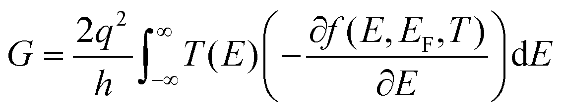 | (1) |
Data availability
The software used for DFT calculations is Quantum ATK.47 The crystal structure used is from the Quantum ATK database. The code for software Atomsk used to create grain boundaries can be found in ref. 48.Conflicts of interest
There are no conflicts to declare.Acknowledgements
We acknowledge the funding from the European Union's Horizon Europe research and innovation program (via CHIPS-JU) under the project ENERGIZE (101194458). This work was also supported by the Spanish Government through the projects PID2023-150162OB-I00 funded by MICIU/AEI/10.13039/501100011033 and FEDER, UE, and CNS2023-143727 RECAMBIO funded by MCIN/AEI/10.13039/501100011033, the European Union NextGeneration EU/PRTR and Consejería de Universidad, Investigación e Innovación de la Junta de Andalucía, through the P21_00149 ENERGHENE research project. F. P. acknowledges the funding from the R + D + i project A-ING-253-UGR23 AMBITIONS co-financed by Consejería de Universidad, Investigación e Innovación and the European Union, under the FEDER Andalucía 2021–2027. Juan J. Palacios acknowledge financial support from the Spanish MICINN (grant no. TED2021-131323B-I00 and PID2022-141712NB-C21), the María de Maeztu Program for Units of Excellence in R&D (grant no. CEX2018-000805-M), the Generalitat Valenciana through the Program Prometeo (2021/017), the Comunidad de Madrid and Spanish State through the Recovery, Transformation and Resilience Plan [Materiales Disruptivos Bidimensionales (2D), MAD2D-CM-UAM7 Materiales Avanzados], and the European Union through the Next Generation EU Funds. Funding for open access charges : University of Granada/CBUA. The views and opinions expressed are those of the authors only and do not necessarily reflect those of the European Union or the European Commission. Neither the European Union nor the European Commission can be held responsible for them.References
- D. Silver, J. Schrittwieser, K. Simonyan, I. Antonoglou, A. Huang, A. Guez, T. Hubert, L. Baker, M. Lai and A. Bolton, et al. , Nature, 2017, 550, 354–359 CrossRef CAS PubMed.
- L. Zhang, J. Tan, D. Han and H. Zhu, Drug Discovery Today, 2017, 22, 1680–1685 CrossRef PubMed.
- M. Milakov, S. H. DevTech and N. Engineer, Deep Learning With GPUs, 2014 Search PubMed.
- K. Roy, A. Jaiswal and P. Panda, Nature, 2019, 575, 607–617 CrossRef CAS PubMed.
- C. Mead and M. Ismail, Analog VLSI implementation of neural systems, Springer Science & Business Media, 1989, vol. 80 Search PubMed.
- J. Zhu, T. Zhang, Y. Yang and R. Huang, Appl. Phys. Rev., 2020, 7, 011312 CAS.
- D. O. Hebb, The organization of behavior; a neuropsychological theory, Wiley, 1949 Search PubMed.
- G. Indiveri and S. C. Liu, Proc. IEEE, 2015, 103, 1379–1397 CAS.
- F. Akopyan, J. Sawada, A. Cassidy, R. Alvarez-Icaza, J. Arthur, P. Merolla, N. Imam, Y. Nakamura, P. Datta, G.-J. Nam, B. Taba, M. Beakes, B. Brezzo, J. B. Kuang, R. Manohar, W. P. Risk, B. Jackson and D. S. Modha, IEEE Trans. Comput.-Aided Des. Integr. Circuits Syst., 2015, 34, 1537–1557 Search PubMed.
- M. Davies, N. Srinivasa, T.-H. Lin, G. Chinya, Y. Cao, S. H. Choday, G. Dimou, P. Joshi, N. Imam, S. Jain, Y. Liao, C.-K. Lin, A. Lines, R. Liu, D. Mathaikutty, S. McCoy, A. Paul, J. Tse, G. Venkataramanan, Y.-H. Weng, A. Wild, Y. Yang and H. Wang, IEEE Micro, 2018, 38, 82–99 Search PubMed.
- E. J. Fuller, Y. Li, C. Bennet, S. T. Keene, A. Melianas, S. Agarwal, M. J. Marinella, A. Salleo and A. A. Talin, IBM J. Res. Dev., 2019, 63, 9:1–9:9 Search PubMed.
- J. Zhu, Y. Yang, R. Jia, Z. Liang, W. Zhu, Z. U. Rehman, L. Bao, X. Zhang, Y. Cai, L. Song and R. Huang, Adv. Mater., 2018, 30, 1–11 Search PubMed.
- M. Jerry, P.-Y. Chen, J. Zhang, P. Sharma, K. Ni, S. Yu and S. Datta, 2017 IEEE International Electron Devices Meeting (IEDM), 2017, pp. 6.2.1–6.2.4.
- S. Herculano-Houzel, Proc. Natl. Acad. Sci. U. S. A., 2012, 109, 10661–10668 CrossRef CAS PubMed.
- Z. Wang, S. Joshi, S. E. Savel'ev, H. Jiang, R. Midya, P. Lin, M. Hu, N. Ge, J. P. Strachan and Z. Li, et al. , Nat. Mater., 2017, 16, 101–108 CrossRef CAS PubMed.
- L. Chua, IEEE Trans. Circuit Theory, 1971, 18, 507–519 Search PubMed.
- S. Choi, J. Yang and G. Wang, Adv. Mater., 2020, 32, 2004659 CrossRef CAS PubMed.
- R. Waser, R. Dittmann, G. Staikov and K. Szot, Adv. Mater., 2009, 21, 2632–2663 CrossRef CAS PubMed.
- F. Zahoor, T. Z. Azni Zulkifli and F. A. Khanday, Nanoscale Res. Lett., 2020, 15, 1–26 CrossRef PubMed.
- H.-S. P. Wong, H.-Y. Lee, S. Yu, Y.-S. Chen, Y. Wu, P.-S. Chen, B. Lee, F. T. Chen and M.-J. Tsai, Proc. IEEE, 2012, 100, 1951–1970 CAS.
- M. Wang, S. Cai, C. Pan, C. Wang, X. Lian, Y. Zhuo, K. Xu, T. Cao, X. Pan and B. Wang, et al. , Nat. Electron., 2018, 1, 130–136 CrossRef CAS.
- F. Hui, E. Grustan-Gutierrez, S. Long, Q. Liu, A. K. Ott, A. C. Ferrari and M. Lanza, Adv. Electron. Mater., 2017, 3, 1600195 CrossRef.
- W. Huh, D. Lee and C.-H. Lee, Adv. Mater., 2020, 32, 2002092 CrossRef CAS PubMed.
- M. D. Ganeriwala, R. Motos Espada, E. G. Marin, J. Cuesta-Lopez, M. Garcia-Palomo, N. Rodríguez, F. G. Ruiz and A. Godoy, ACS Appl. Mater. Interfaces, 2024, 16, 49724–49732 CrossRef CAS PubMed.
- M. Yang, X. Zhao, Q. Tang, N. Cui, Z. Wang, Y. Tong and Y. Liu, Nanoscale, 2018, 10, 18135–18144 RSC.
- R. Ge, X. Wu, M. Kim, J. Shi, S. Sonde, L. Tao, Y. Zhang, J. C. Lee and D. Akinwande, Nano Lett., 2018, 18, 434–441 CrossRef CAS PubMed.
- F. Ducry, D. Waldhoer, T. Knobloch, M. Csontos, N. Jimenez Olalla, J. Leuthold, T. Grasser and M. Luisier, npj 2D Mater. Appl., 2022, 6, 58 CrossRef CAS.
- R. Xu, H. Jang, M.-H. Lee, D. Amanov, Y. Cho, H. Kim, S. Park, H.-j. Shin and D. Ham, Nano Lett., 2019, 19, 2411–2417 CrossRef CAS PubMed.
- Y. Shi, C. Pan, V. Chen, N. Raghavan, K. L. Pey, F. M. Puglisi, E. Pop, H.-S. P. Wong and M. Lanza, 2017 IEEE International Electron Devices Meeting (IEDM), 2017, pp. 5.4.1–5.4.4.
- M. Farronato, P. Mannocci, M. Melegari, S. Ricci, C. M. Compagnoni and D. Ielmini, Adv. Mater., 2023, 35, 2205381 CrossRef CAS PubMed.
- R. Ge, X. Wu, L. Liang, S. M. Hus, Y. Gu, E. Okogbue, H. Chou, J. Shi, Y. Zhang, S. K. Banerjee, Y. Jung, J. C. Lee and D. Akinwande, Adv. Mater., 2021, 33, 2007792 CrossRef CAS PubMed.
- V. K. Sangwan, D. Jariwala, I. S. Kim, K.-S. Chen, T. J. Marks, L. J. Lauhon and M. C. Hersam, Nat. Nanotechnol., 2015, 10, 403–406 CrossRef CAS PubMed.
- H. Mehrer, Diffusion in solids: fundamentals, methods, materials, diffusion-controlled processes, Springer Science & Business Media, 2007, vol. 155 Search PubMed.
- M. Li, H. Liu, R. Zhao, F.-S. Yang, M. Chen, Y. Zhuo, C. Zhou, H. Wang, Y.-F. Lin and J. J. Yang, Nat. Electron., 2023, 6, 491–505 CrossRef CAS.
- S. Bhattacharjee, E. Caruso, N. McEvoy, C. Ó. Coileáin, K. O'Neill, L. Ansari, G. S. Duesberg, R. Nagle, K. Cherkaoui, F. Gity and P. K. Hurley, ACS Appl. Mater. Interfaces, 2020, 12, 6022–6029 CrossRef CAS PubMed.
- S. Mitra and S. Mahapatra, npj 2D Mater. Appl., 2024, 8, 26 CrossRef CAS.
- W. Zhou, X. Zou, S. Najmaei, Z. Liu, Y. Shi, J. Kong, J. Lou, P. M. Ajayan, B. I. Yakobson and J.-C. Idrobo, Nano Lett., 2013, 13, 2615–2622 CrossRef CAS PubMed.
- X. Zou, Y. Liu and B. I. Yakobson, Nano Lett., 2013, 13, 253–258 CrossRef CAS PubMed.
- P. Man, D. Srolovitz, J. Zhao and T. H. Ly, Acc. Chem. Res., 2021, 54, 4191–4202 CrossRef CAS PubMed.
- S. Smidstrup, A. Pedersen, K. Stokbro and H. Jónsson, J. Chem. Phys., 2014, 140, 214106 CrossRef PubMed.
- R. A. De Souza, in Ion Transport in Metal Oxides, John Wiley & Sons, Ltd, 2016, ch. 5, pp. 125–164 Search PubMed.
- G. Boschetto, S. Carapezzi, C. Delacour, M. Abernot, T. Gil and A. Todri-Sanial, ACS Appl. Nano Mater., 2022, 5, 10192–10202 CrossRef CAS.
- D. M. Guzman, N. Onofrio and A. Strachan, J. Appl. Phys., 2017, 121, 055703 CrossRef.
- P. Wu, N. Yin, P. Li, W. Cheng and M. Huang, Phys. Chem. Chem. Phys., 2017, 19, 20713–20722 RSC.
- X. Sun, Z. Wang and Y. Q. Fu, Sci. Rep., 2015, 5, 18712 CrossRef CAS PubMed.
- W. Shi, Z. Wang, Z. Li and Y. Fu, Mater. Chem. Phys., 2016, 183, 392–397 CrossRef CAS.
- S. Smidstrup, T. Markussen, P. Vancraeyveld, J. Wellendorff, J. Schneider, T. Gunst, B. Verstichel, D. Stradi, P. A. Khomyakov and U. G. Vej-Hansen, et al. , J. Phys.: Condens. Matter, 2019, 32, 015901 CrossRef PubMed.
- P. Hirel, Comput. Phys. Commun., 2015, 197, 212–219 CrossRef CAS.
Footnote |
| † Electronic supplementary information (ESI) available. See DOI: https://doi.org/10.1039/d4nr05321d |
| This journal is © The Royal Society of Chemistry 2025 |