
 Open Access Article
 This Open Access Article is licensed under a Creative Commons Attribution-Non Commercial 3.0 Unported Licence
Tuning the electronic properties of ZnO nanofilms via strain-induced structural phase transformations and quantum confinement†
Raul
Morales-Salvador
a,
Ilker
Demiroglu
 b,
Francesc
Viñes
a and
Stefan T.
Bromley
*ac
b,
Francesc
Viñes
a and
Stefan T.
Bromley
*ac
aDepartament de Ciència de Materials i Química Física & Institut de Química Teòrica i Computacional (IQTC), Universitat de Barcelona, c/Martí i Franquès 1-11, 08028 Barcelona, Spain. E-mail: s.bromley@ub.edu
bDepartment of Advanced Technologies, Eskisehir Technical University, 2 Eylül kampüsü, 26555 Eskişehir, Turkey
cInstitució Catalana de Recerca i Estudis Avançats (ICREA), Passeig de Lluís Companys, 23, 08010 Barcelona, Spain
First published on 27th February 2025
Abstract
ZnO nanostructures have huge potential in a wide range of technologies, including photocatalysis, optoelectronics, and energy harvesting. ZnO commonly exhibits the wurtzite polymorphic phase (wz-ZnO) and is one of the few inorganic materials where nanoscale structural phase engineering has revealed alternative polymorphs. These structurally novel nanophases also have properties (e.g. mechanical, electronic) that differ from those of wz-ZnO, and thus may pave the way to new applications. Here, we follow a strain-induced transformation between the body centred cubic phase (BCT-ZnO) and the graphitic phase (g-ZnO), which has been experimentally demonstrated in ZnO nanowires. Using free-standing ZnO nanofilms as a reference nanosystem, we use density functional theory based calculations to follow the BCT-ZnO ↔ g-ZnO phase transformation relative to systematic changes in the in-plane biaxial strain and nanofilm thickness. Compressive strain favours the BCT-ZnO phase, whereas tensile strain induces the transformation to the g-ZnO phase. As the applications of nanoscale ZnO usually take advantage of its semiconducting nature, we mainly focus on the variance of the band gap and the character of the band edges. Our work features the use of Crystal Orbital Hamilton Population (COHP) analysis, which helps provide a uniquely detailed understanding of this complex nanosystem based on orbital overlap. We use this approach to reveal how strain and quantum confinement (through the nanofilm thickness) have distinct and significant effects on the structural and electronic properties of both BCT-ZnO and g-ZnO phases. The latter phase is particularly interesting as it involves a subtle competition between two structural sub-phases (the layered-ZnO and hex-ZnO phases). These two phases can be distinguished by their respective orbital overlap characteristics which, in turn, can be finely tuned by strain and thickness. We propose that the rich electronic properties of this nanosystem can be interpreted through a monolayer superlattice model in which localised surface states and more spatially delocalised quantum confined states compete. More generally, our work illustrates how the intricate interplay of strain, quantum confinement and structural phase transformations in an inorganic nanosystem can be analysed and understood through the use of COHP analysis of orbital overlap contributions.
Introduction
Nanoscale materials often exhibit different crystalline atomic ordering (i.e. polymorphs) from those observed in the respective macroscopic solids.1 The structures and properties of low dimensional nanomaterials (e.g. nanofilms, nanowires) can also be tuned by mechanical strain.2 Combining size and strain thus provides a flexible approach for structural phase engineering of nanomaterials in which emergent properties (e.g. mechanical, electronic) can lead to new applications.3 Here, we focus on zinc oxide (ZnO) which is highly amenable to nanostructuring4 and has huge potential in a wide range of nanoscale applications (e.g. photocatalysis, optoelectronics, energy harvesting).5 ZnO is also one of the very few inorganic materials for which nanoscale phase engineering has been experimentally demonstrated using both size6 and strain.7 ZnO has thus become an archetypal system for theoretically predicting the viability of new stable polymorphic phases by system size reduction8–14 and/or by nanostructuring.15–18The possibility of novel nano-stabilised structural phases in ZnO started with the theoretical prediction of a so-called graphitic polymorph (g-ZnO) in unsupported nanofilms,8 which was subsequently confirmed in experiments on metal-supported ZnO nanofilms.6 The g-ZnO phase consists of a–b planar (ZnO)3-based hexagonally ordered layers stacked in the c direction. We note that unlike graphite, which has a staggered AB stacking of hexagonal layers, g-ZnO exhibits an eclipsed AA stacking. For free-standing nanofilms, g-ZnO is predicted to be the most energetically stable ZnO polymorph for stacks of up to three planar hexagonal layers (i.e. N ≤ 3 layers). g-ZnO nanofilms have attracted interest with respect to possible chemical applications (e.g. strain-thickness reactivity control,19,20 CO2 photoreduction21). However, such studies rarely consider the possibility of transformations to other competing polymorphic phases.
For nanofilms with N ≥ 4, it becomes more energetically favourable for the layers in the g-ZnO phase to slightly buckle and bond with one another. The different possible nanofilm polymorphs available at this structural phase transformation can be enumerated by systematically varying the bonding patterns between stacked hexagonal layers while maintaining the AA stacking of g-ZnO.9 For four layers, the lowest energy polymorphs resulting from this search are found to be a class of polytypes based on the body centred cubic phase (BCT-ZnO).9 This finding is in line with other studies where the transformation from g-ZnO to BCT-ZnO in nanofilms with N = 4–16 has been calculated to be effectively barrierless at finite temperatures.11,13
The BCT-ZnO phase is also predicted to be more stable than pristine wz-ZnO in c-oriented freestanding nanofilms with N ≤ 27.11 The relatively low stability of c-oriented wz-ZnO nanofilms in this thickness range is due to the energetically costly electronic imbalance induced by the terminating (0001) and (000![[1 with combining macron]](https://www.rsc.org/images/entities/char_0031_0304.gif) ) polar surfaces.13,22 Calculations of nanofilms possessing pristine as-cut polar surfaces will attempt to compensate this imbalance by internal charge transfer from one polar surface to another leading to spurious surface metallisation.13 This is a relatively inefficient stabilization mechanism and clean (i.e. ligand-free) ZnO polar surfaces are instead experimentally observed to structurally reconstruct to achieve stabilization.23,24 Increasing the stability of polar wz-ZnO nanofilms by surface reconstruction lowers the thickness at which the stability crossover to BCT-ZnO occurs to between 14 and 16 layers.9 For c-oriented wz-ZnO nanofilms that are thinner than this threshold, it is more effective to stabilize the system via a phase transformation of the whole nanofilm to a non-polar structure. For the thinnest nanofilms, this transformation is found to be spontaneous, with pristine wz-ZnO nanofilms directly relaxing to the g-ZnO structure for N ≤ 4 and to BCT-ZnO for N = 5–6 layers.11 Thicker wz-ZnO nanofilm layers with approximately N = 7–16 are metastable in 0 K calculations, but are likely to be thermally or mechanically susceptible to phase transformations to more stable non-polar phases such as BCT-ZnO. In principle, there are some non-polar nanofilm structures that are theoretically predicted to be slightly energetically more stable than BCT-ZnO at 0 K, for the thickness range N = 7–16. However, the transformations to such structures from BCT-ZnO have relatively high associated barriers.13 As such, the relatively easier transitions between g-ZnO/wz-ZnO and BCT-ZnO are likely to dominate in ZnO nanomaterials for moderate temperatures and/or mechanically induced phase transformations.
) polar surfaces.13,22 Calculations of nanofilms possessing pristine as-cut polar surfaces will attempt to compensate this imbalance by internal charge transfer from one polar surface to another leading to spurious surface metallisation.13 This is a relatively inefficient stabilization mechanism and clean (i.e. ligand-free) ZnO polar surfaces are instead experimentally observed to structurally reconstruct to achieve stabilization.23,24 Increasing the stability of polar wz-ZnO nanofilms by surface reconstruction lowers the thickness at which the stability crossover to BCT-ZnO occurs to between 14 and 16 layers.9 For c-oriented wz-ZnO nanofilms that are thinner than this threshold, it is more effective to stabilize the system via a phase transformation of the whole nanofilm to a non-polar structure. For the thinnest nanofilms, this transformation is found to be spontaneous, with pristine wz-ZnO nanofilms directly relaxing to the g-ZnO structure for N ≤ 4 and to BCT-ZnO for N = 5–6 layers.11 Thicker wz-ZnO nanofilm layers with approximately N = 7–16 are metastable in 0 K calculations, but are likely to be thermally or mechanically susceptible to phase transformations to more stable non-polar phases such as BCT-ZnO. In principle, there are some non-polar nanofilm structures that are theoretically predicted to be slightly energetically more stable than BCT-ZnO at 0 K, for the thickness range N = 7–16. However, the transformations to such structures from BCT-ZnO have relatively high associated barriers.13 As such, the relatively easier transitions between g-ZnO/wz-ZnO and BCT-ZnO are likely to dominate in ZnO nanomaterials for moderate temperatures and/or mechanically induced phase transformations.
The favoured wz-ZnO phase in macroscopic systems has a relatively high density. Thus, accessing lower density polymorphs, such as g-ZnO and BCT-ZnO, from wz-ZnO by mechanical means implies the need for significant negative pressures (i.e. tensile strain).25–27 The inherent favorability of BCT-ZnO and g-ZnO in nanosized systems and the easier application of uniaxial/biaxial tensile stress in low dimensional nanostructures (e.g. 1D nanowires, 2D nanofilms) thus provide opportunities for stress-induced phase control. We also note that with decreasing size, nanomaterials also tend to have fewer structural defects and are thus less susceptible to structural failure under stress.28 Experimentally, uniaxially stressed wz-ZnO nanowires are indeed found to display a reversible phase transformation between BCT-ZnO and g-ZnO (hex-ZnO), where the BCT-ZnO phase is predicted to become dominant.7 Computational modelling studies have also reported similar phase transformations to BCT-ZnO in nanowire systems, induced by either uniaxial strain29 or bending.30 Reversible phase transformations between wz-ZnO and BCT-ZnO phases have also been experimentally observed in the outer few layers of non-polar surfaces of wz-ZnO nano-islands.31
Considering the technological potential of nano-ZnO and the experimentally confirmed nanoscale stabilisation and structural interconversion of g-ZnO and BCT-ZnO polymorphs, it is important to understand the properties of this phase-reversible nanosystem. Here, we provide a systematic study of how the g-ZnO ↔ BCT-ZnO phase transformation can be engineered by both biaxial strain and thickness in ZnO nanofilms. We specifically focus on how the electronic structure varies during these size/strain-induced structural changes. By carefully analysing the respective roles of orbital overlap and quantum confinement, we show that this phase-tunable semiconductor nanofilm system allows for highly controllable band gaps and band edges which could open the door to new applications.
Models and computational details
We consider isolated periodic slab models to represent free-standing nanofilms of both g-ZnO and BCT-ZnO. This choice avoids the fact that the differing basal plane symmetries of g-ZnO and BCT-ZnO tend to inhibit their phase interconversion when epitaxially supported.32,33N-Layer (hereon abbreviated as NL) slab models with N = 3–6, 8, 10, 12, 14, and 16 were considered. For both polymorphs, p(2 × 2) supercells were used, where each layer is composed of four Zn and four O atoms. To avoid spurious inter-slab interactions, models were isolated in the c-direction normal to the slab surface by a periodic vacuum spacing of 10 Å.For few-layer g-ZnO, the interaction between aligned hexagonal layers is non-bonded, as in graphite. However, a very similar phase has been reported with bonded interactions between layers.9 Although these two forms of g-ZnO are often conflated in the literature, herein we highlight their distinct properties and how they can be revealed and controlled during phase transformations. When required, we distinguish the g-ZnO form with non-bonded layers as the layered phase (layered-ZnO) and the more strongly bound version as the hexagonal phase (hex-ZnO). The models of all considered phases are shown in Fig. 1.
 | ||
| Fig. 1 Atomic positions for two layers of BCT-ZnO (upper) and the layered- and hex-forms of g-ZnO (lower). Grey lines indicate the boundary of the periodic simulation cell (left: in-plane view, right: c-axis view). The listed numbers of layers (N) for each case indicates the thickness range for which the respective structure could be stabilised for some range of in-plane biaxial strain. Atom colour key: Zn – grey, O – red. | ||
To calculate the optimized structures and properties of the three phases, periodic density functional theory (DFT) based calculations were carried out using the Perdew–Burke–Ernzerhof (PBE)34 functional by means of the VASP code.35,36 We note that the PBE functional has been previously shown to be reliable for evaluating pressure-induced phase transitions between ZnO polymorphs.37–39 The underestimation of electronic band gaps when using the PBE functional is approximately corrected using a fitted relation between band gap values as calculated using PBE and an accurate many body G0W0 method for a range of ZnO polymorphs.18 The projector augmented wave approach40 was used to describe the core electron density, with all d electrons included for Zn atoms. The valence electron density was expanded in a plane wave basis set with a cut-off energy of 500 eV. The Brillouin zone integration was sampled using a 3 × 3 × 1 Monkhorst–Pack k-grid.41 The threshold for the electronic convergence criterion was set to 10−4 eV, and geometry optimizations were considered converged when forces acting on atoms were below 0.01 eV Å−1. For calculating band structures, single point calculations of optimised nanofilm structures were employed using a 9 × 9 × 1 Monkhorst–Pack k-grid. Convergence tests for the chosen calculation parameters can be found in the ESI†.
For each slab, the in-plane cell parameters were constrained in a range of fixed values to model a range of in-plane biaxial strains between −10% (i.e. compression) and +10% (i.e. tension). For each strain, the coordinates of all atoms and the out-of-plane c-parameter of the supercell were allowed to fully relax without symmetry constraints.
To analyse the bonding in the studied polymorphs, we employed COHP (Crystal Orbital Hamilton Population) analysis42,43 as implemented in the LOBSTER code.44 This methodology partitions the energy of electronic bands into contributions from overlapping orbitals. Specifically, for orbitals centred on neighbouring atoms, COHP provides a quantitative measure of energy-lowering bonding (negative) contributions and energy-raising antibonding (positive) contributions. Note that energetically neutral non-bonding makes a zero COHP contribution. Consequently, energy-resolved COHP analyses provide a way to interpret band structures in terms of local chemical interactions.
For a more detailed analysis of chemical bonding, the COHP approach can be directionally resolved whereby the energy of a given band is decomposed into individual contributions from each k-point. The resulting k-COHP analysis mathematically distinguishes between on-site and off-site contributions in the following way:
 | (1) |
 | (2) |
 | (3) |
 | (4) |
Results and discussion
Using the above-described slab models, we systematically vary the nanofilm thickness and in-plane strain. For all considered thicknesses, a polymorphic g-ZnO ↔ BCT-ZnO phase transformation is also observed within the range of in-plane strain considered. Below, we follow how these three interacting factors lead to complex changes in energetic stability, structure and electronic properties.Structure and energetics
In Fig. 2 we plot the calculated relative energy of the in-plane strained ZnO nanofilms of varying thickness with respect to the energy of bulk BCT-ZnO. For each thickness we define zero strain at the point of minimum energy on each relative energy curve, which in all cases corresponds to the fully relaxed BCT-ZnO phase. With increasing nanofilm thickness, the curves progressively shift to lower energies, indicating an expected stabilisation towards the corresponding bulk phase. For in-plane compression up to −8% the BCT-ZnO phase remains structurally stable for all nanofilm thicknesses. Under in-plane biaxial tension, the BCT-ZnO phase is susceptible to a phase transformation to the g-ZnO phase. We note that there is no obvious sign of differentiation between the layered- and hex-forms of the g-ZnO phase in the relative energy curves. For the thinnest 3L BCT-ZnO slab, we find that the transformation to g-ZnO can be achieved with +1.3% strain. However, with increasing thickness the strain required to induce the transformation increases to approximately +5.5% for the thickest 16L nanofilm. This change is in-line with the increasing energy difference between the BCT-ZnO and g-ZnO phases with increasing thickness. Apart from the thinnest 3L nanofilm, the strain-induced BCT-ZnO → g-ZnO transformation for thicker nanofilms leads to an increasingly positively strained g-ZnO phase with respect to its minimum energy on an extrapolated energy versus strain curve. This implies that it would be difficult to stabilise fully relaxed g-ZnO nanofilms due to their mechanical instability to transform into the BCT-phase. We note that systematic computational exploration of biaxially strained nanofilms can be used to search for such instabilities and thus find new polymorphic phases in a simulated mechanical annealing approach.46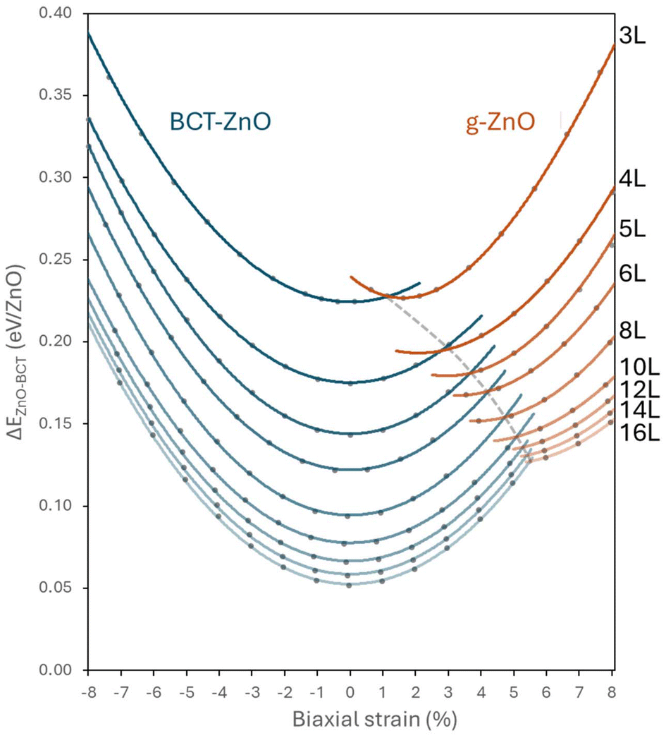 | ||
| Fig. 2 Relative energy (relative to bulk BCT-ZnO per ZnO unit) of nanofilms with respect to varying in-plane biaxial strain and nanofilm thickness. Solid lines are guide to the eye and follow the calculated black data points. Blue lines follow data points corresponding to the BCT-ZnO phase and orange lines follow data points corresponding to the g-ZnO phase. The dashed grey line follows the strain/thickness conditions at the BCT-ZnO ↔ g-ZnO energetic stability transition. | ||
For a better understanding of how to physically induce the BCT-ZnO and g-ZnO phase transformation by applying tensile stress, we have calculated the in-plane biaxial modulus for the 5L nanofilm to be 138.5 GPa. This would imply that a tensile stress of 1.4 GPa would be needed for each +1% of biaxial strain of the 5L BCT-ZnO nanofilm. This is comparable to 5–15 GPa of uniaxial tensile stress used in experiments on ZnO nanowires to induce BCT-ZnO phase transformations with the corresponding strains of approximately 2–5%.7
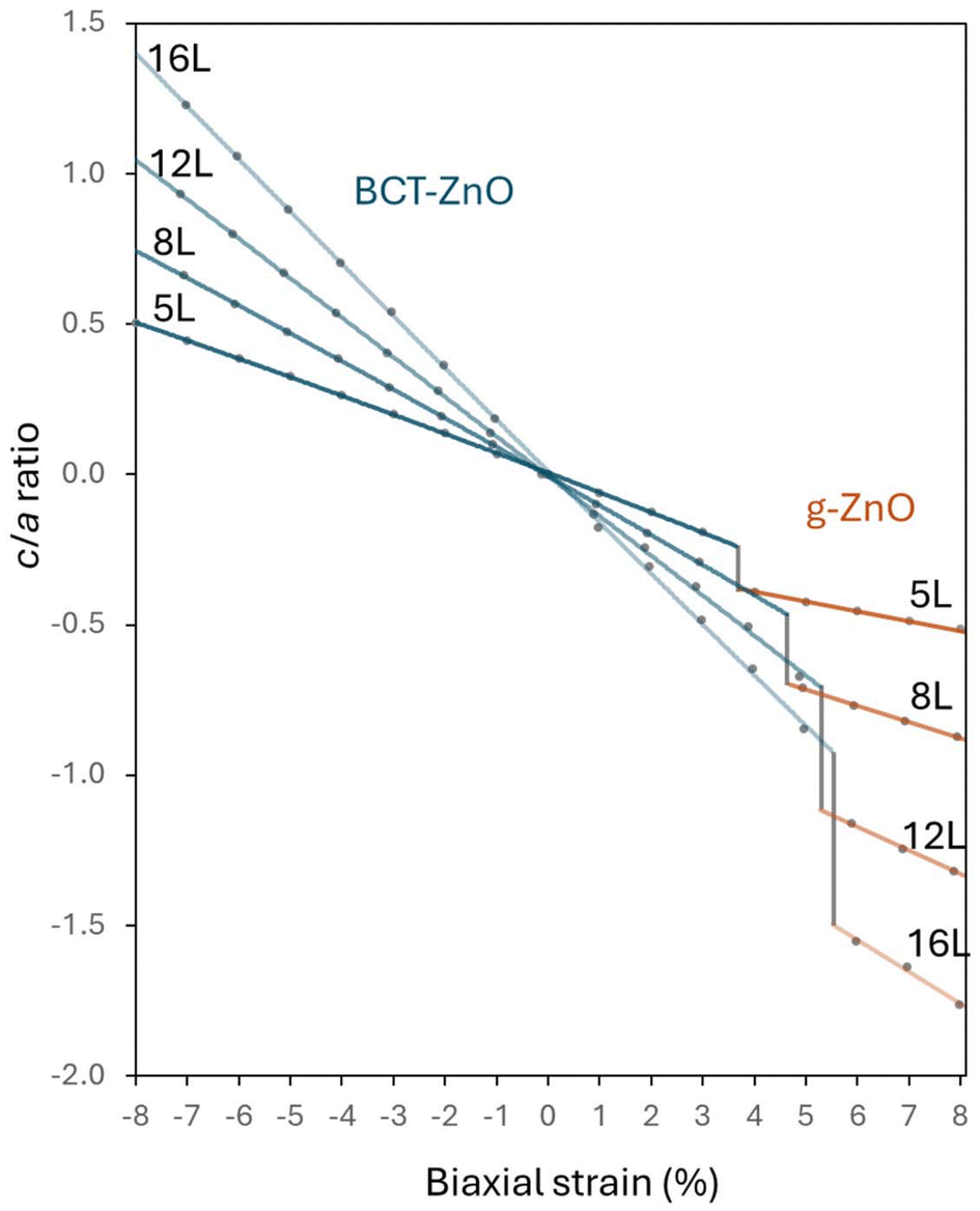
In Fig. 3, we follow how the c/a lattice parameter ratio varies with respect to in-plane strain for selected representative nanofilm thicknesses of N = 5, 8, 12, 16. For the data corresponding to the BCT-ZnO phase, the nanofilms show a monotonic linear decrease of their c/a ratio from an in-plane compression of −8% up until the tensile strain corresponding to the transformation to the g-ZnO phase. At this point the c/a ratio abruptly decreases and then continues to decrease linearly with a slightly shallower slope. Increasing the nanofilm thickness results in progressively steeper slopes of the linear trends in the c/a ratio for both phases. For materials with a positive Poisson ratio, increasing the a and b parameters via in-plane tensile strain will cause a corresponding reduction in the c-parameter, and vice versa. We note that, as for the energetic stability (see Fig. 2), the strain/thickness-dependent tendencies of the c/a ratio in the region of g-ZnO stability show no obvious signs of distinct hex-ZnO and layered-ZnO forms.
 | ||
| Fig. 3 Dependence of the c/a ratio on in-plane strain for four selected nanofilm thicknesses. Solid lines are guide to the eye and follow the calculated black data points. Blue lines follow data points corresponding to the BCT-ZnO phase and orange lines follow data points corresponding to the g-ZnO phase. | ||
From an atomistic perspective, in-plane compression of the unstrained BCT-ZnO phase tends to increase the buckling of the a–b layers while maintaining the bonding connectivity of the BCT phase. However, in-plane tensile strain leads to more complex bonding changes. In Fig. 4, we examine the strain-induced structural response of the g-ZnO phase from a chemical bonding perspective for the thinnest 3L system. Increasing tensile strain on the unstrained BCT-ZnO phase will first tend to flatten the a–b layers favouring the transition to the layered ZnO. For the 3L system, this occurs at +1% strain where the average interlayer spacing has its maximum of 2.43 Å. At this point, a COHP analysis of the Zn 4s–O 2s bonding (see insets to Fig. 4) shows that the in-plane bonding contribution is larger than the out-of-plane bonding contribution. Although increasing the in-plane strain increases the in-plane Zn–O bond distances and quickly brings the layers closer together, the dominance of in-plane bonding over out-of-plane bonding persists until a strain of +6%. Here, the interlayer spacing is reduced by 0.2 Å to 2.25 Å, at which the out-of-plane bonding COHP contribution becomes equal to the respective in-plane contribution. A further increase in strain results in a more gradual linear decrease in the interlayer spacing where the out-of-plane bonding COHP contribution dominates, indicating the transition to the hex-ZnO phase with interlayer Zn–O bonds. A similarly large difference in interlayer spacing between relaxed 6L layered-ZnO films (2.37 Å) and the bulk hex-ZnO phase (2.25 Å) is reported in ref. 47 (where both phases are referred to as the h-BN phase), where it is noted that this structural response is inverse to that found in non-layered ZnO nanofilms. This behaviour also suggests that out-of-plane uniaxial compression in the c-direction would also be a possible means to control the BCT-ZnO ↔ layered-ZnO/hex-ZnO phase transformation in this system. Indeed, several DFT studies have examined how uniaxial compression in the c-direction can induce wz-ZnO → g-ZnO phase transformations in the bulk48 and in nanowires.9,49 For progressively thicker nanofilms, the strain-induced BCT-ZnO → g-ZnO transformation occurs when the g-ZnO phase is increasingly positively strained relative to its most relaxed structure. As such, the range of strain for which the layered-ZnO phase can be stabilised by tensile strain rapidly reduces with nanofilm thickness.
 | ||
| Fig. 4 Dependence of average interlayer spacing on in-plane strain for the 3L system. The inset plots show the characteristic in-plane (red) and out-of-plane (blue) bonding COHP contributions for different strain regimes. | ||
Electronic structure
 | ||
| Fig. 5 Variation of Egapversus biaxial strain. The PBE-calculated Egap values have been corrected following the approach in ref. 18. The orange shaded area indicates the approximate region of stability of the layered-ZnO phase. | ||
Upon the strain-induced phase transformation to the layered-ZnO phase, the Egap values for each nanofilm sharply increase. This increase ranges from approximately +0.4 eV for the thickest films to approximately +0.15 eV for the 3L nanofilm. Like the BCT-ZnO phase, the layered-ZnO phase has a direct band gap at the gamma point in reciprocal space. In the range of strains for which different nanofilms exhibit a stable layered-ZnO phase, the Egap values are relatively stable, with only small gap decreases with increasing positive strain. Further positive strain leads to a transformation of all nanofilms to the hex-ZnO phase. It is found that the layered-ZnO → hex-ZnO phase transformation is also linked to an electronic transition from a direct to indirect band gap. The transformation to the hex-ZnO phase also marks a significant increase in the rate of Egap magnitude reduction with increasing in-plane tension.
The transition from a direct (layered-ZnO) to an indirect gap (hex-ZnO) can be understood due to the strain-dependent competition between in-plane and out-of-plane Zn–O antibonding bands in the two respective materials (see above). Each of these bands gives rise to two distinct O 2p contributions to the VBM at k-points Γ and T. Competition between in-plane and out-of-plane antibonding causes corresponding changes in the VBM and a shift between a direct gap (layered-ZnO) and an indirect band gap (hex-ZnO). In Fig. 6, we show this situation with bands calculated for the 5L nanofilm case. Here, the red band has its main contribution at Γ from antibonding orbital overlap from in-plane Zn–O bonds. Conversely, at T, antibonding overlap from out-of-plane Zn–O bonds is the major contributor to the green band. With an increase of tensile biaxial strain, the in-plane Zn–O bond lengths are increased (reducing antibonding overlap) which lowers the energy of the red band. At the same time, the interlayer spacing decreases which shortens the out-of-plane Zn–O distances (see Fig. 4), which tends to increase the anti-bonding overlap and increase the energy of the green band. Eventually, with sufficient in-plane strain, this tendency leads to a transition from a direct bandgap in the layered-ZnO phase to an indirect gap in the hex-ZnO phase. During this transition, the CBM, which is associated with isotropic Zn 4s–O 2s antibonding, is stabilised more by the strain-induced increase of in-plane Zn–O separations than the destabilisation from the smaller decrease in interlayer spacing. This CBM stabilization is the main reason for the decrease in Egap in the hex-ZnO phase with increasing biaxial tension.
 | ||
| Fig. 6 Calculated band structures during the strain-induced layered-ZnO → hex-ZnO phase transformation of a 5L nanofilm. The three colours correspond to the three labelled dominant antibonding orbital contributions at T (green band) and Γ (blue and red bands). The correspondingly coloured numbers indicate the energetic antibonding k-COHP contributions at these k-points for each band. | ||
Starting from a relaxed flat ZnO monolayer, a relatively large positive biaxial strain (8%) has been predicted to be needed to induce a transition from a direct to an indirect gap.50 Unlike in the presently reported nanofilms, the lack of interlayer interactions in monolayers makes the destabilisation of the out-of-plane antibonding states more difficult to achieve. DFT calculations have also been used to study the effect of uniaxial out-of-plane tension on the bulk hex-ZnO phase to induce a phase transformation to the layered phase with a concomitant direct to indirect Egap transition.51 A related direct to indirect change in Egap has also been reported in DFT studies of the uniaxial compression-induced wz-ZnO → hex-ZnO transition.48,49 We note that this subtle transition has also been studied with DFT calculations using hybrid functionals,51 which confirms that it is not related to the underestimation of Egap magnitudes by GGA functionals.
In Fig. 7, we provide an overview of how the relative energies of the CBM and VBM vary with in-plane biaxial strain with respect to the unstrained case, for all considered nanofilm thicknesses. Nanofilms of all thicknesses exhibit similar general trends with respect their strain-response of CBM and VBM energies, whereby negative strain (i.e. in-plane compression) tends to be destabilising and positive strain (i.e. in-plane tension) tends to be stabilising. For the negatively strained regime, where the BCT-ZnO polymorph is favoured, both the VBM and CBM energies increase with increasing in-plane compression for all thicknesses. Here, the VBM is always destabilised more than the CBM (i.e. blue bars higher than red bars in Fig. 7) which causes the observed bandgap reduction compared to the corresponding unstrained case (see Fig. 5). In BCT-ZnO, the VBM is dominated by contributions from in-plane antibonding orbital overlap, as also found for the layered-ZnO and hex-ZnO polymorphs (see above).
 | ||
| Fig. 7 Variation of the energy of the VBM (blue bars) and CBM (red bars) with respect to in-plane biaxial strain for all considered nanofilm thicknesses. The energy variation is taken with respect to the VBM and CBM of the corresponding unstrained nanofilm for each thickness. | ||
For the positively strained regime in which g-ZnO (i.e. layered-ZnO or hex-ZnO phases) is favoured, for all thicknesses the energy of the CBM (red bars in Fig. 7) gradually decreases with increasing strain. The energy of the VBM, however, is relatively less affected with respect to that of the corresponding unstrained system for all thicknesses. So, for g-ZnO, the energetic stabilisation of the CBM at Γ with increasing biaxial in-plane tension is mainly responsible for the observed strain-induced Egap reduction (see Fig. 5).
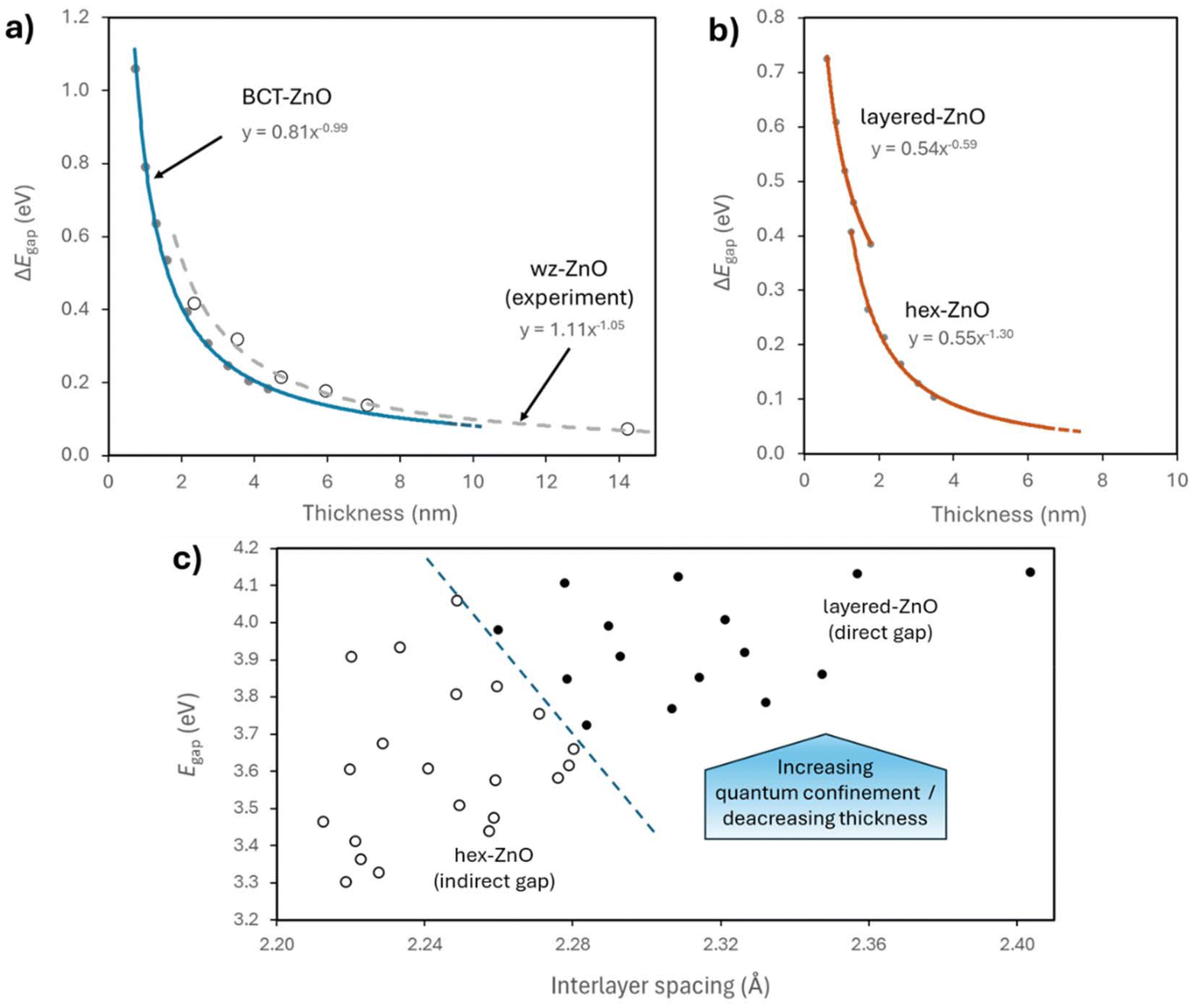 | ||
| Fig. 8 Variance in ΔEgap values with respect to: (a) nanofilm thickness for the BCT-ZnO nanofilms at 0% strain (all thicknesses) and experimentally prepared wz-ZnO nanofilms (from ref. 54), (b) nanofilm thickness for the layered-ZnO nanofilms at 4% strain (for 3L–8L) and the hex-ZnO nanofilms at 6% strain (for 6L–16L), and (c) interlayer spacing for the layered-ZnO and hex-ZnO phases for a selected range of strains and thicknesses. | ||
The observed QC effect is found to be due to an increase in the energy of the CBM when the nanofilm thickness decreases. Conversely, the VBM is found to be hardly affected by changes in nanofilm thickness. This contrasting behaviour is in-line with the difference in the effective masses of excited electrons (in the CBM) and holes (in the VBM) in these systems. With a lower effective mass, the respective charge carriers become more mobile (delocalised) and are thus more susceptible to the effects of spatial confinement. Likewise, charge carriers with a higher effective mass are less affected by QC. Generally, wz-ZnO systems are known to have relatively light electrons and heavy holes.57 We thus expect that thickness-induced QC should have a significantly stronger effect on the energy of the CBM than on the energy of the VBM in these nanofilms, as confirmed in Fig. 9. We note that a similar effect has been reported in DFT calculations of group III–V semiconductor nanofilms.58 Nanoporosity is also known to affect the CBM much more than the VBM in ZnO.18 For BCT-ZnO, the QC-induced Egap variation is contrary to that induced by in-plane strain, which is mainly due to relatively large changes in the energy of the VBM. However, for g-ZnO both QC and strain mainly affect the CBM which dominates the observed Egap variations.
 | ||
| Fig. 9 Variance in CBM and VBM energies with respect to nanofilm thickness for BCT-ZnO nanofilms with 0% in-plane biaxial strain and hex-ZnO nanofilms with 6% in-plane biaxial strain. | ||
 | ||
| Fig. 10 Per-layer summed atomic k-COHP contributions to the VBM of 5L, 10L and 16L nanofilms (top to bottom) and −10%, 0% and +3% in-plane biaxial strains (left to right). Contributions are expressed as a percent of the total absolute contribution. The x-axes follow the order of the layers in the out-of-plane c direction from one outermost layer (Out.) toward the innermost layer (Inn.) and to the other outermost layer (Out.). In each case the nanofilm thickness is provided in nm. | ||
In Fig. 11, we compare how the summed atomic k-COHP contributions to the CBM for each layer vary for the three nanofilm thicknesses under increasing tensile in-plane biaxial strains. For most of these systems the hex-ZnO phase is favoured, apart from the +4% strained 5L nanofilm, for which the layered-ZnO phase is more energetically stable. For this case, the in-plane contributions to the CBM involving unoccupied Zn 4s and O 2s orbitals are much larger than the respective out-of-plane contributions. In the absence of significant interlayer interactions all layers are essentially independent and the k-COHP analysis in Fig. 11 shows that the contribution for each layer is very similar. This situation gradually changes with increases in thickness and/or biaxial strain but implies that the CBM for the layered phase is less susceptible to QC (see Fig. 8). With increasing in-plane biaxial tension (to +9% and +14%), the layers in the 5L system are forced to be closer together. This causes a phase transformation to the hex-ZnO polymorph and an increase in out-of-plane anti-bonding Zn 4s–O 2s contributions to the CBM. Antibonding interactions are less destabilising in situations of reduced orbital overlap and thus their k-COHP contributions are dominant for the outer layers of the highly strained 5L system.
 | ||
| Fig. 11 Per-layer summed atomic k-COHP contributions to the CBM of nanofilms with 5L for +4%, +9% and +14% in-plane biaxial strains and for 10L and 16L thicknesses and +6%, +11% and +16% in-plane biaxial strains. The contributions per-layer are expressed as a percent of the total absolute contribution. The x-axes follow the order of the layers in the out-of-plane c direction from one outermost layer (Out.) toward the innermost layer (Inn.) and to the other outermost layer (Out.). In each case the nanofilm thickness is provided in nm. | ||
On increasing the thickness, for the highest +16% strained 10L and 16L hex-ZnO nanofilms, we find a similar situation to the more strained hex-ZnO 5L systems, where near surface anti-bonding Zn 4s–O 2s contributions dominate the CBM. For lower biaxial strains, however, we see the emergence of a similar distinct pattern of k-COHP contributions to the CBM for both the 10L and 16L systems. For the +11% strained systems we still see the Zn 4s–O 2s antibonding contributions but together with a set of contributions which increase from the outermost layers to the innermost layer. For the +6% strained systems, the latter contributions dominate, and surface contributions are the lowest. The k-COHP analysis shows that these contributions come from the bonding overlap of unoccupied Zn 4s–Zn 4s orbitals (see Fig. S1 in the ESI†). In these nanofilm systems, all layers have significant contributions which vary in a regular layer dependent manner. This implies that the role of each layer and how they interact with each other need to be considered when interpreting how the CBM contributions are distributed throughout these nanofilms. From our analysis above (see Fig. 8 and 9), we know that the CBM in hex-ZnO nanofilms is strongly affected by QC, in line with its multi-layer spatially distributed k-COHP contributions. The pattern of CBM contributions also implies that QC is felt progressively more strongly going from outer layers to inner layers. This cumulative effect suggests that each layer is incrementally contributing to the overall QC effect. We propose an interpretation of this situation from the perspective of a monolayer superlattice (i.e. a quasi-2D layered system of intercoupled monolayer quantum wells).58,59
Monolayer superlattices are typically composed of stacks of single layers of a semiconducting material, which are interleaved with layers of another material to modulate the interactions between the semiconducting monolayers. In our case, the degree of biaxial strain modulates the interactions between ZnO monolayers in the g-ZnO system. Taking the +6% 10L case as an example, the CBM corresponds to a wavefunction (WF) that is dominated by interlayer bonding interactions. Treating each ZnO monolayer as a quantum well leads to discretisation of the effect of QC on this WF. Starting from outside the system, the WF has its minimum magnitude, and will then increase when entering the first monolayer well. When moving to the next monolayer, the interlayer coupling will determine the degree of WF decay, and thus the magnitude of the WF in the next ZnO layer. When the decay is less than 100%, the WF magnitude will increase in a step-wise layer-by-layer manner until the middle of the nanofilm and then, by symmetry, will decay again in the same manner to the farthest outer surface of the nanofilm. In this way, QC acts on the ful nanofilm system but is modulated depending on the interlayer coupling. Such a discretised layer-dependent WF is schematically shown in Fig. 12a. These results show that hex-ZnO can be thought of as a monolayer superlattice in which in-plane biaxial strain can significantly modulate the interlayer coupling. Upon increased biaxial strain there is a gradual transition from Zn 4s–Zn 4s interlayer bonding overlap to anti-bonding Zn 4s–O 2s overlap. Upon the corresponding interior-to-surface shift in the character of the WF, transmission of QC to the system is diminished (Fig. 12b and c). This shows that the electronic response of g-ZnO nanofilms can be sensitively tuned by strain and thickness. In particular, the ability to shift between surface states and QC-susceptible states in such quasi-2D nanofilms could open up new application potential (e.g. sensing, catalysis, optoelectronics).
 | ||
| Fig. 12 Schematic representation of the relative magnitude of the Zn 4s–Zn 4s bonding (blue) and Zn 4s–O 2s antibonding (red) contributions to a monolayer superlattice WF associated with the CBM for the 10L hex-ZnO system for +6% (a), +11% (b) and +16% (c) in-plane biaxial strain (also see Fig. 11). The black line denotes the energy profile of a series of quantum wells, approximately corresponding to the ZnO monolayers in the 10L nanofilm, each separated by a finite barrier. The x-axes follow the order of the layers in the out-of-plane c direction from one outermost layer (Out.) toward the innermost layer (Inn.) and to the other outermost layer (Out.). | ||
Conclusions
We provide a detailed investigation of the structural and electronic properties of ZnO nanofilms with thicknesses from 3L to 16L, for a wide range of compressive and tensile biaxial strains. This parameter regime allows us to follow the experimentally confirmed strain-induced BCT-ZnO ↔ g-ZnO polymorphic phase transition. Our study features the application of COHP-based analysis to understand this complex inorganic nanosystem. Such an approach allows for an orbital level system characterisation and, as far as we are aware, has not previously been applied to analyse nanoscale phase transformations. For all considered film thicknesses and compressive strains, BCT-ZnO is the most stable polymorphic phase. With tensile biaxial strain, the barrierless structural transformation to the g-ZnO polymorphic phase is favoured. Generally, with sufficient positive or negative biaxial strain, the Egap of the unstrained nanofilms is reduced. Likewise, the increase in nanofilm thickness also leads to an Egap decrease. Our COHP-based analysis provides several detailed insights into the intimate relationship between structure, bonding and electronic properties. We highlight, for example, that all three of these properties serve to distinguish the quasi-2D layered-ZnO phase from the 3D hex-ZnO phase, both often collectively referred to as the g-ZnO phase. For strains favouring the g-ZnO phase, variations in the CBM underpin the strain-related change in Egap. However, for the BCT-ZnO dominated strain/thickness regime, the VBM mainly determines the strain-dependent changes in Egap. With respect to increases in nanofilm thickness, for both BCT-ZnO and g-ZnO, the Egap reduction is mainly due to QC acting on the CBM. We use layer-by-layer k-COHP-based analysis to reveal the detailed nature of the CBM and VBM, thus elucidating their respective susceptibility to QC and strain. This analysis reveals that the CBM in g-ZnO nanosystems can be sensitively tuned by strain and/or thickness between: i) being dominated by QC-resistant localised surface contributions, and ii) having a QC-dependent spatially-distributed character. The competition between these two regimes can be rationalised from a monolayer superlattice perspective. Here, the electronic state can be tuned by the degree of strain/thickness-dependent interlayer interactions and their bonding or antibonding character, rather than by fixed intervening barrier layers. This dramatic superlattice-based electronic tunability is likely to be general to many inorganic nanofilms that exhibit quasi-2D structural phases and could pave the way to a range of new applications (e.g. photocatalysis, optoelectronics, sensors).Author contributions
S. T. B. formulated the original research concept and directed the project. R. M. S. and I. D. performed the DFT calculations. R. M. S. performed the COHP calculations. R. M. S. and S. T. B. performed the formal analyses/interpretation of the results and prepared the original draft of the paper. All authors contributed to the discussion of the results and the revision of the final draft.Data availability
Data for this article, including VASP OUTCAR files and optimised atomic coordinates for all nanofilms considered are available at the NOMAD repository at https://doi.org/10.17172/NOMAD/2024.12.06-3.Conflicts of interest
There are no conflicts to declare.Acknowledgements
Support is acknowledged from the MICINN-funded PID2021-127957NB-I00, PID2021-126076NB-I00, TED2021-129506B-C22, and TED2021-132550B-C21 project grants, and the Maria de Maeztu program for Spanish Structures of Excellence (CEX2021-001202-M) and project grants 2021SGR00354 and 2021SGR00079 funded by the Generalitat de Catalunya. F. V. thanks the ICREA Academia Award 2023 Ref. Ac2216561. I. D. acknowledges support from the Eskisehir Technical University (ESTÜ-BAP-21GAP085).References
- A. Navrotsky, Energetic clues to pathways to biomineralization: Precursors, clusters, and nanoparticles, Proc. Natl. Acad. Sci. U. S. A., 2004, 101, 12096 CrossRef CAS PubMed.
- S. Yang, F. Liu, C. Wu and S. Yang, Tuning surface properties of low dimensional materials via strain engineering, Small, 2016, 12, 4028–4047 CrossRef CAS PubMed.
- Q. Yun, et al., Recent Progress on Phase Engineering of Nanomaterials, Chem. Rev., 2023, 123, 13489–13692 CrossRef CAS PubMed.
- Z. L. Wang, Nanostructures of zinc oxide, Mater. Today, 2004, 7, 26–33 CrossRef CAS.
- S. Rahaa and M. Ahmaruzzaman, ZnO nanostructured materials and their potential applications: progress, challenges and perspectives, Nanoscale Adv., 2022, 4, 1868–1925 RSC.
- C. Tusche, H. L. Mayerheim and J. Kirschner, Observation of Depolarized ZnO(0001) Monolayers: Formation of Unreconstructed Planar Sheets, Phys. Rev. Lett., 2007, 99, 026102 CrossRef CAS PubMed.
- P. Zhao, X. Guan, H. Zheng, S. Jia, L. Li, H. Liu, L. Zhao, H. Sheng, W. Meng, Y. Zhuang, J. Wu, L. Li and J. Wang, Surface- and Strain-Mediated Reversible Phase Transformation in Quantum-Confined ZnO Nanowires, Phys. Rev. Lett., 2019, 123, 216101 CrossRef CAS PubMed.
- C. L. Freeman, F. Claeyssens, N. L. Allan and J. H. Harding, Graphitic nanofilms as precursors to wurtzite films: theory, Phys. Rev. Lett., 2006, 96, 066102 CrossRef PubMed.
- A. J. Kulkarni, M. Zhou, K. Sarasamak and S. Limpijumnong, Novel Phase Transformation in ZnO Nanowires under Tensile Loading, Phys. Rev. Lett., 2006, 97, 105502 CrossRef PubMed.
- L. Zhang and H. Huang, Structural transformation of ZnO nanostructures, Appl. Phys. Lett., 2007, 90, 023115 CrossRef.
- B. J. Morgan, Preferential stability of the d-BCT phase in ZnO thin films, Phys. Rev. B: Condens. Matter Mater. Phys., 2009, 80, 174105 CrossRef.
- I. Demiroglu and S. T. Bromley, Nanofilm versus Bulk Polymorphism in Wurtzite Materials, Phys. Rev. Lett., 2013, 110, 245501 CrossRef PubMed.
- F. Viñes, O. Lamiel-Garcia, F. Illas and S. T. Bromley, Size dependent structural and polymorphic transitions in ZnO: from nanocluster to bulk, Nanoscale, 2017, 9, 10067–10074 RSC.
- S. Conejeros, N. L. Allan, F. Claeyssens and J. N. Hart, Graphene and novel graphitic ZnO and ZnS nanofilms: the energy landscape, nonstoichiometry and water dissociation, Nanoscale Adv., 2019, 1, 1924 RSC.
- J. Carrasco, F. Illas and S. T. Bromley, Ultralow-Density Nanocage-Based Metal-Oxide Polymorphs, Phys. Rev. Lett., 2007, 99, 235502 CrossRef PubMed.
- M. A. Zwijnenburg, F. Illas and S. T. Bromley, Apparent Scarcity of Low-Density Polymorphs of Inorganic Solids, Phys. Rev. Lett., 2010, 104, 175503 CrossRef PubMed.
- M. A. Zwijnenburg and S. T. Bromley, Structure direction in zinc oxide and related materials by cation substitution: an analogy with zeolites, J. Mater. Chem., 2011, 21, 15255 RSC.
- I. Demiroglu, S. Tosoni, F. Illas and S. T. Bromley, Bandgap engineering through nanoporosity, Nanoscale, 2014, 6, 1181–1187 RSC.
- L. Lin, Z. Zeng, Q. Fu and X. Bao, Strain and support effects on phase transition and surface reactivity of ultrathin ZnO films: DFT insights, AIP Adv., 2020, 10, 125125 CrossRef CAS.
- L. Lin, Z. Zeng, Q. Fu and X. Bao, Achieving flexible large-scale reactivity tuning by controlling the phase, thickness and support of two-dimensional ZnO, Chem. Sci., 2021, 12, 15284 RSC.
- Y. Zhao, N. Liu, S. Zhou and J. Zhao, Two-dimensional ZnO for the selective photoreduction of CO2, J. Mater. Chem. A, 2019, 7, 16294–16303 RSC.
- B. Meyer and D. Marx, Density-functional study of the structure and stability of ZnO surfaces, Phys. Rev. B: Condens. Matter Mater. Phys., 2003, 67, 035403 CrossRef.
- G. Kresse, O. Dulub and U. Diebold, Competing stabilization mechanism for the polar ZnO (0001)-Zn surface, Phys. Rev. B: Condens. Matter Mater. Phys., 2003, 68, 245409 CrossRef.
- D. Mora-Fonz, T. Lazauskas, M. R. Farrow, C. R. A. Catlow, S. M. Woodley and A. A. Sokol, Why are polar surfaces of ZnO stable?, Chem. Mater., 2017, 29, 5306 CrossRef CAS.
- L.-Z. Xu, Y.-L. Liu, H.-B. Zhou, L.-H. Liu, Y. Zhang and G.-H. Lu, Ideal strengths, structure transitions, and bonding properties of a ZnO single crystal under tension, J. Phys.: Condens. Matter, 2009, 21, 495402 CrossRef PubMed.
- W. Sangthong, J. Limtrakul, F. Illas and S. T. Bromley, Predicting transition pressures for obtaining nanoporous semiconductor polymorphs: oxides and chalcogenides of Zn, Cd and Mg, Phys. Chem. Chem. Phys., 2010, 12, 8513–8520 RSC.
- D. Zagorac, J. C. Schön, J. Zagorac and M. Jansen, Prediction of structure candidates for zinc oxide as a function of pressure and investigation of their electronic properties, Phys. Rev. B: Condens. Matter Mater. Phys., 2014, 89, 075201 CrossRef.
- B. Wei, K. Zheng, Y. Ji, Y. Zhang, Z. Zhang and X. Han, Size-Dependent Bandgap Modulation of ZnO Nanowires by Tensile Strain, Nano Lett., 2012, 12, 4595–4599 CrossRef CAS PubMed.
- J. Wang, A. J. Kulkarni, K. Sarasamak, S. Limpijumnong, F. J. Ke and M. Zhou, Molecular dynamics and density functional studies of a body-centered-tetragonal polymorph of ZnO, Phys. Rev. B: Condens. Matter Mater. Phys., 2007, 76, 172103 CrossRef.
- J. Zhang, Phase transformation and its effect on the piezopotential in a bent zinc oxide nanowire, Nanotechnology, 2021, 32, 075404 CrossRef CAS PubMed.
- M.-R. He, R. Yu and J. Zhu, Reversible Wurtzite–Tetragonal Reconstruction in ZnO(10–10) Surfaces, Angew. Chem., Int. Ed., 2012, 51, 7744–7747 CrossRef CAS PubMed.
- B. Morgan, First-principles study of epitaxial strain as a method of B4→BCT stabilization in ZnO, ZnS, and CdS, Phys. Rev. B: Condens. Matter Mater. Phys., 2010, 82, 153408 CrossRef.
- D. Wu, M. G. Lagally and F. Liu, Stabilizing Graphitic thin films of wurtzite materials by epitaxial strain, Phys. Rev. Lett., 2011, 107, 236101 CrossRef PubMed.
- J. P. Perdew, K. Burke and M. Ernzerhof, Generalized Gradient Approximation Made Simple, Phys. Rev. Lett., 1996, 77, 3865 CrossRef CAS PubMed.
- G. Kresse and J. Furthmüller, Efficiency of Ab initio Total Energy Calculations for Metals and Semiconductors Using a Plane-Wave Basis Set, Comput. Mater. Sci., 1996, 6, 15–50 CrossRef CAS.
- G. Kresse and J. Furthmüller, Efficient Iterative Schemes for Ab Initio Total-Energy Calculations Using a Plane-Wave Basis Set, Phys. Rev. B: Condens. Matter Mater. Phys., 1996, 54, 11169–11186 CrossRef CAS PubMed.
- M. Kalaya, H. H. Karta, S. Ö. Karta and T. Çağın, Elastic properties and pressure induced transitions of ZnO polymorphs from first-principle calculations, J. Alloys Compd., 2009, 484, 431–438 CrossRef.
- J. E. Jaffe, J. A. Snyder, Z. Lin and A. C. Hess, LDA and GGA calculations for high-pressure phase transitions in ZnO and MgO, Phys. Rev. B: Condens. Matter Mater. Phys., 2000, 62, 1660 CrossRef CAS.
- M. P. Molepo and D. P. Joubert, Computational study of the structural phases of ZnO, Phys. Rev. B: Condens. Matter Mater. Phys., 2011, 84, 094110 CrossRef.
- P. E. Blöch, Projector Augmented-Wave method, Phys. Rev. B: Condens. Matter Mater. Phys., 1994, 50, 17953 CrossRef PubMed.
- H. J. Monkhorst and J. D. Pack, Special Points for Brillouin-Zone Integrations, Phys. Rev. B, 1976, 13, 5188 CrossRef.
- R. Dronskowski and P. E. Blöchl, Crystal Orbital Hamilton Populations (COHP). Energy-Resolved Visualization of Chemical Bonding in Solids based on Density-Functional Calculations, J. Phys. Chem., 1993, 97, 8617–8624 CrossRef CAS.
- S. Maintz, V. L. Deringer, A. L. Tchougreeff and R. Dronskowski, Analytic Projection from Plane-Wave and PAW Wavefunctions and Application to Chemical-Bonding Analysis in Solids, J. Comput. Chem., 2013, 34, 2557–2567 CrossRef CAS PubMed.
- S. Maintz, V. L. Deringer, A. L. Tchougreeff and R. Dronskowski, LOBSTER: A tool to extract chemical bonding from plane-wave based DFT, J. Comput. Chem., 2016, 37, 1030–1035 CrossRef CAS PubMed.
- X. Peng, Q. Wei and A. Copple, Strain-Engineered Direct-Indirect Band Gap Transition and Its Mechanism in Two-Dimensional Phosphorene, Phys. Rev. B: Condens. Matter Mater. Phys., 2014, 90, 085402 CrossRef CAS.
- S. M. Kozlov, I. Demiroglu, K. M. Neyman and S. T. Bromley, Reduced ceria nanofilms from structure prediction, Nanoscale, 2015, 7, 4361 RSC.
- L. Sponza, J. Goniakowski and C. Noguera, Confinement effects in ultrathin ZnO polymorph films: Electronic and optical properties, Phys. Rev. B, 2016, 93, 195435 CrossRef.
- Y. Wanga, W. Tang, J. Zhu and J. Liu, Strain induced change of band structure and electron effective mass in wurtzite ZnO: A first-principles study, Comput. Mater. Sci., 2015, 145–149 CrossRef.
- Y. Zhang, Y.-H. Wen, J.-C. Zheng and Z.-Z. Zhuc, Direct to indirect band gap transition in ultrathin ZnO nanowires under uniaxial compression, Appl. Phys. Lett., 2009, 94, 113114 CrossRef.
- R. Das, B. Rakshit, S. Debnath and P. Mahadevan, Microscopic model for the strain-driven direct to indirect band-gap transition in monolayer MoS2 and ZnO, Phys. Rev. B: Condens. Matter Mater. Phys., 2014, 89, 115201 CrossRef.
- B. Rakshit and P. Mahadevan, Indirect to direct bandgap transition under uniaxial strain in layered ZnO, Appl. Phys. Lett., 2013, 102, 143116 CrossRef.
- E. Inico, C. Saetta and G. Di Liberto, Impact of quantum size effects to the band gap of catalytic materials: a computational perspective, J. Phys.: Condens. Matter, 2024, 36, 361501 CrossRef CAS PubMed.
- N. S. Mohammad, Understanding quantum confinement in nanowires: basics, applications and possible laws, J. Phys.: Condens. Matter, 2014, 26, 423202 CrossRef PubMed.
- P. Zhang, Z. Liu, W. Duan, F. Liu and J. Wu, Topological and electronic transitions in a Sb(111) nanofilm: The interplay between quantum confinement and surface effect, Phys. Rev. B: Condens. Matter Mater. Phys., 2012, 85, 201410(R) CrossRef.
- A. Barnasas, N. Kanistras, A. Ntagkas, D. I. Anyfantis, A. Stamatelatos, V. Kapaklis, N. Bouropoulos, E. Mystiridou, P. Poulopoulos, C. S. Garoufalis and S. Baskoutas, Quantum confinement effects of thin ZnO films by experiment and theory, Phys. E, 2020, 120, 114072 CrossRef CAS.
- L. Sponza, J. Goniakowski and C. Noguera, Structural, electronic, and spectral properties of six ZnO bulk polymorphs, Phys. Rev. B: Condens. Matter Mater. Phys., 2015, 91, 075126 CrossRef.
- H. Morkoç and Ü. Özgür, Zinc Oxide: Fundamentals, Materials and Device Technology, Wiley, Germany, 2008 Search PubMed.
- L. A. Cipriano, G. Di Liberto, S. Tosoni and G. Pacchioni, Quantum confinement in group III–V semiconductor 2D nanostructures, Nanoscale, 2020, 12, 17494 RSC.
- S. Y. Ren, Two types of electronic states in one-dimensional crystals of finite length, Ann. Phys., 2002, 301, 22–30 CAS.
- P. Pereyra, The transfer matrix method and the theory of finite periodic systems. From heterostructures to superlattices, Phys. Status Solidi B, 2022, 259, 2100405 CrossRef CAS.
Footnote |
| † Electronic supplementary information (ESI) available. See DOI: https://doi.org/10.1039/d4nr05206d |
| This journal is © The Royal Society of Chemistry 2025 |