
Epitaxial growth of antiferromagnetic MnBi2Te4/CdTe heterostructures on GaAs(001) using molecular beam epitaxy: structure and electronic properties
Wesley F.
Inoch
a,
Gilberto
Rodrigues-Junior
a,
S. L. A.
Mello
 a,
S.
de Castro
b,
M. L.
Peres
b,
Sukarno O.
Ferreira
a,
Ângelo
Malachias
c,
Maybi F.
Sampaio
d,
Olavo
Teixeira Neto
d,
Bráulio S.
Archanjo
d and
Leonarde N.
Rodrigues
*a
a,
S.
de Castro
b,
M. L.
Peres
b,
Sukarno O.
Ferreira
a,
Ângelo
Malachias
c,
Maybi F.
Sampaio
d,
Olavo
Teixeira Neto
d,
Bráulio S.
Archanjo
d and
Leonarde N.
Rodrigues
*a
aDepartamento de Física, Instituto de Ciências Exatas (ICE), Universidade Federal de Viçosa, Viçosa, Minas Gerais 36570-900, Brasil. E-mail: leonarde.rodrigues@ufv.br
bInstituto de Física e Química, Universidade Federal de Itajubá, Itajubá, Minas Gerais 37500-903, Brasil
cDepartmento de Física, Instituto de Ciências Exatas (ICEx), Universidade Federal de Minas Gerais (UFMG), Av. Antônio Carlos, 6627, Belo Horizonte, Minas Gerais 30123-970, Brasil
dInstituto Nacional de Metrologia, Qualidade e Tecnologia (Inmetro), Divisão de Materiais (DIMAT), Xerém, 25250-020, Rio de Janeiro, Brasil
First published on 14th March 2025
Abstract
MnBi2Te4 is one of the most recent materials that integrates the class of topological quantum materials exhibiting topological insulating properties and magnetic ordering, thus providing the opportunity to investigate particular topological quantum states and design novel spintronic devices. The samples were grown on GaAs(100) substrates using molecular beam epitaxy with Bi2Te3, Te and Mn as sources. The growth was characterized through X-ray diffraction, atomic force microscopy and transmission electron microscopy. Topological insulator properties were probed through scanning tunneling microscopy and scanning tunneling spectroscopy, while antiferromagnetic order was investigated via magnetotransport measurements. Furthermore, we propose a high-quality CdTe thin film as a cap layer to protect topological surface states, thus opening the possibility of integrating topological quantum materials with group II–VI semiconductors via van der Waals epitaxy.
 Leonarde N. Rodrigues | Leonarde do Nascimento Rodrigues received his doctoral degree from Federal University of Juiz de Fora, Juiz de Fora, Brazil, in 2016. He is currently Professor in the Physics Department at the Federal University of Viçosa, Brazil. His main current research area is the conventional epitaxial growth of semiconductor heterostructures and thin films, van der Waals epitaxial growth of chalcogenide materials, fabrication of semiconductor nanomembranes and devices and their characterization via high resolution X-ray diffraction and optical spectroscopy for inelastic light scattering and photoluminescence applications. |
Introduction
Novel materials exhibiting exotic states of matter, such as topological insulators (TIs), have attracted considerable attention in solid-state physics in the last decades.1 The quantum spin Hall effect observed in HgTe quantum wells2 grown via molecular beam epitaxy (MBE) confirmed typical TI behavior with protected conductor surface states due to spin–orbit coupling and time-reversal symmetry. Such characteristics make this material a promising candidate for sophisticated spintronic devices and quantum computation applications.3 In recent years, the combination of topological insulation properties with magnetic ordering has enabled the emergence of a new class of topological quantum materials.4 The magnetic moment provides mass to the otherwise massless Dirac fermions, thus opening an energy gap and allowing topologically driven quantum states to emerge in the system.5 Exotic states of matter such as quantum anomalous Hall effect (QAHE)6 insulators and axion insulators7 have been observed as a response to the coexistence between magnetism and topological insulator state.Magnetically doped topological insulators, such as Cr- and V-doped (Bi,Sb)2Te3, present the QAHE.8 However, the temperature to measure the effect is <1 K owing to structural defects in the Bi2Te3 crystal introduced by dopants. Magnetic topological insulators such as MnBi2Te4 with antiferromagnetic order9 are an alternative to magnetically doped TIs since they are expected to exhibit the QAHE at relatively high temperatures, thus enabling device applications. The QAHE has also been predicted for thin films/flakes of MnBi2Te4-family compounds.10
Quantum transport properties of MnBi2Te4 have been exploited to achieve the QAHE at zero magnetic field in thin film samples grown via MBE.9 Recently, a study addressed QAHE results11 to clarify the controversial data available. Although the QAHE has been reported in thin flakes6 of MnBi2Te4 and giant nonlocal transport signals in the axion insulator state,12 a thin film grown via MBE does not present limitations with the control in the fabrication of the film shape and does not have the size limitation as in the case of exfoliated flakes. The reproducibility and control of composition and thickness positions the MBE growth technique as an appropriate choice to achieve the fabrication of large-area and high-quality topological magnetic devices.9,11 Previous works in this field have been performed using the MBE growth of MnBi2Te4 on different substrates such as BaF2(111),13 sapphire(0001),11 Si(111),14 Al2O3(0001),15 SrTiO3(111)16 and GaAs(111)B.17 A common link between these works is the use of two effusion cells containing Bi2Te3 and MnTe or three effusion cells containing Te, Bi and Mn. The former13 basically controls the beam equivalent pressure between Bi2Te3 and MnTe. Other works,15,17 since MnBi2Te4 is sensitive to the Bi![[thin space (1/6-em)]](https://www.rsc.org/images/entities/char_2009.gif) :Mn flux ratio, provide the fine stoichiometry tuning of MnBi2Te4, controlling each source individually. Some approaches may follow a more complex routine involving growth and annealing of a Bi2Te3 buffer layer.17
:Mn flux ratio, provide the fine stoichiometry tuning of MnBi2Te4, controlling each source individually. Some approaches may follow a more complex routine involving growth and annealing of a Bi2Te3 buffer layer.17
Although van der Waals (vdW) material growth conditions are challenging considering weak interlayer forces, good quality systems can be grown via MBE, despite the large lattice mismatch between the film and substrate.18 Careful control of growth conditions is necessary for the formation of correct stoichiometry and phase. In this work, MnBi2Te4 thin films were directly grown on a GaAs(001) substrate using molecular beam epitaxy. GaAs is a suitable substrate choice used in spintronics and can be a platform for integrating topological insulator devices.19 The growth recipe used here is similar to that reported previously20 for the growth of Bi2Te3 using one additional Mn effusion cell. This versatile control can allow the growth of heterostructures and superstructures such as Bi2Te3/MnBi2Te4 with only three effusion cells. To avoid the exposure of topological insulators to air and prevent the degradation of surface states, we grew a CdTe cap layer on top of the MnBi2Te4 film, substituting the usually used Te cap because the metallic Te layer would work as a transport channel, masking the transport that occurs through the MnBi2Te4 film.21 This high-resistivity CdTe layer opens the possibility to integrate TIs with II-VI heterostructures. The morphological and structural properties of MnBi2Te4 are characterized using atomic force microscopy (AFM), high resolution X-ray diffraction (HRXRD) and high-resolution transmission electron microscopy (HRTEM). Topological surface state properties were studied using scanning tunneling spectroscopy (STS), thus providing information about the surface local density of states (LDOS). To verify the antiferromagnetic order and electronic properties of MnBi2Te4, magnetoresistance and van der Pauw measurements were conducted.
Experimental
Bi2Te3 and MnBi2Te4 were grown using a custom-built molecular beam epitaxy (MBE) system on undoped GaAs(001) substrates. Before growth, the substrate was annealed at 580 °C for 5 min to completely remove native oxide. Standard effusion cells containing high-purity powders of Bi2Te3, Te, Mn, and CdTe were used for growth. Growth parameters were the same as those already reported20 for the growth of Bi2Te3, with the addition of a Mn source. Unlike previously mentioned works on the growth of MnBi2Te4 on different substrates, our growth recipe uses independent sources of Bi2Te3, Te and Mn. The same beam fluxes of Bi2Te3 and Te were maintained by adjusting the same deposition rate grown at room temperature and measuring the thickness of pure Bi2Te3 and Te films. The MnBi2Te4 structure (deposition rate of approximately 0.5 nm min−1) was reached using pure Mn evaporated from an effusion cell with an optimized temperature of 840 °C. The substrate temperature used was 380 °C for MnBi2Te4 and CdTe thin films. High-purity polycrystalline CdTe was evaporated from single effusion cells with a deposition rate of approximately 3 nm min−1. The base pressure never exceeded 10−8 Torr. Bi2Te3 samples were grown for comparison. To avoid the exposure of the topological insulator to air, we grew an undoped 60 nm-thick CdTe cap layer on top of the MnBi2Te4 film. The crystalline structure of the Bi2Te3 and MnBi2Te4 films was investigated through high-resolution X-ray diffraction (HRXRD) using a four-circle Bruker D8-discover diffractometer equipped with Cu Kα (λ = 1.54056 Å) radiation source and a 2-bounce Ge (220) monochromator. The deposition rate and interface roughness were estimated using X-ray reflectometry (XRR) measurements. XRR fits using the Parratt formalism22 or the available algorithm23 allows the evaluation of the layer thickness and interface roughness of the deposited layer. AFM measurements were carried out using a FlexAFM Nanosurf microscope operating in a tapping (semi-contact) mode with controlled humidity maintained below 30%. Cross-sectional focused ion beam (FIB) thin lamellae were prepared using an FEI Helios Nanolab 650 DualBeam system, with final polishing conducted at 2 keV and a 7° tilt to minimize amorphization caused by the Ga FIB. Scanning transmission electron microscopy (STEM) was performed using a Cs probe-corrected Titan 80-300 (FEI Company) transmission electron microscope operating at 300 kV. The microscope was equipped with a conventional high-angle annular dark-field (HAADF) detector and an Oxford Aztec Energy TEM advanced microanalysis system. STM and STS measurements were performed under ultra-high vacuum conditions in an Omicron-VT STM system operating at room temperature, with a base pressure of 1.0 × 10⁻¹⁰ mbar. All STM images were acquired using electrochemically etched polycrystalline W tips in a constant current mode, and for STS measurements, a lock-in amplifier (operating a 3000 Hz) was used to obtain differential conductance (dI/dV) curves. All STS curves considered here were an average of at least 30 curves taken at the same point. For STS measurements, the samples were capped with Te and immediately exfoliated in vacuum before STS measurements. For magnetotransport measurements, electrical contacts in the van der Pauw geometry were soldered using indium droplets. This procedure was performed using a hot plate at 180 °C for 2 min to guarantee that the diffusion occurs through the layers. The measurements were carried out using the physical properties measurement system (PPMS) from Quantum Design, equipped with a helium-cooled superconducting system with a magnetic field of up to 9 T that operates over a broad temperature range from 1.9 to 400 K. A standard four-probe AC lock-in technique with a constant excitation current of 10 μA was employed.Results and discussion
Fig. 1(a) and (e) show the XRR data for Bi2Te3 and MnBi2Te4 thin films without the CdTe cap layer, with experimental data shown as a black circle and the fitting curve as a blue line. Both samples exhibited well-defined fringes, indicating a uniform film thickness and smooth surface and interface across the substrate area. The model parameters yielded a Bi2Te3 film thickness of 47.3 nm and surface roughness of 2.6 nm. The MnBi2Te4 film had a similar thickness of 48.2 nm with a surface roughness of approximately 10% smaller than Bi2Te3. The comparable film thickness resulted from using the same growth time and parameters for the Bi2Te3 and Te effusion cells. The fitting curves were obtained using the bulk material density, and results were in good agreement with experimental results, suggesting that a stoichiometric phase was achieved.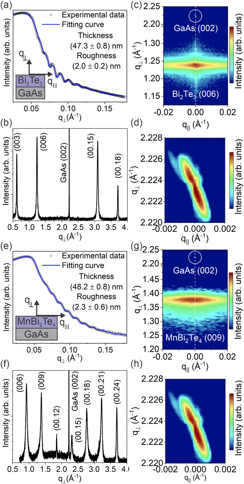 | ||
| Fig. 1 Structural comparison of Bi2Te3 and MnBi2Te4 TI. (a) and (e): XRR spectra for Bi2Te3 and MnBi2Te4. Black circles represent the experimental data, while blue lines represent the fitting curve. (b) and (f): HRXRD measurements for the [0001] direction for Bi2Te3 and MnBi2Te4. (c) and (g): reciprocal space mapping around Bi2T3(006) and MnBi2Te4(009) reflections and GaAs(002) as a reference indicated by a circle. (d) and (h) Show the RSM around GaAs(002) from (c) and (g), respectively. | ||
Fig. 1(b) and (f) show symmetrical HRXRD scans for 47 nm Bi2Te3 and 48 nm MnBi2Te4 thick films, respectively. In addition to the peaks belonging to the GaAs substrate, it is possible to observe only the (0 0 3n) peaks as labeled in the figure, indicating that both films grew epitaxially on the GaAs substrate. Fig. 1(c) and (g) show the reciprocal space maps (RSMs) acquired near the symmetric Bi2Te3 (006) and MnBi2Te4 (009) diffraction peak, respectively, and the (002) diffraction peak of the GaAs as a reference (indicated by the circle). Note that the (002) diffraction peak of GaAs is a nearly perfect single crystal, which reflects the discrepancy between the width of the Bi2Te3 and MnBi2Te4 films and the GaAs substrate as can be observed on the RSM around GaAs (002) in Fig. 1(d) and (h). The vertical alignment between the Bi2Te3 and MnB2Te4 films and GaAs indicates well-oriented growth with reflections in the (003n) parallel plane. The distortion of GaAs reflection on the RSM originates from the resolution limit of the equipment. The out-of-plane direction reveals symmetric oscillation patterns that confirm the smooth surfaces and a well-ordered structure. In-plane direction has an intense diffuse scattering, indicating the presence of defects in the structure, such as mosaicity, due to the large lattice mismatch. The out-of-plane direction of the MnBi2Te4(009) RSM, shown in Fig. 1(g), is asymmetric with a more pronounced broadening at lower values of reciprocal space. The in-plane diffraction has a FWHM that is twice as large as that of Bi2Te3, indicating a larger defect density. Stacking errors may be responsible for the asymmetric behavior and the broadening of the diffraction peaks.
Fig. 2(a, b) and (e, f) shows AFM images (5 × 5 μm2) and (1 × 1 μm2) for the Bi2Te3 and MnBi2Te4 thin films, respectively. The images are presented using a shading effect that highlights step-like features, such as the triangular terraces that are typical of Bi2Te3 samples,20 as shown in Fig. 2(b). These triangular structures are also observed on the surface of the MnBi2Te4 film, as shown in Fig. 2(c), but lack distinct steps and reach a height of up to 20 nm. The presence of triangular shapes on the surface indicates regions where adatoms have less mobilities and thus form clusters, already observed in others van der Waals materials.24 The van der Waals growth mode allows growth with good out-of-plane orientation even in a large mismatch substrate such as cubic GaAs. However, the in-plane rotation responsible for the defects observed in the RSM can be easily identified by the misalignment of the triangular features shown in Fig. 2(a, b) and (e, f) for Bi2Te3 and MnBi2Te4, respectively. The red dotted lines in HRTEM images of Fig. 2(c) and (g) indicate the quintuple layer (QL) of Bi2Te3 and the septuple layer (SL) of MnBi2Te4. Fig. 2(d) and (h) are higher resolution images showing details of the QL (Te–Bi–Te–Bi–Te) and SL (Te–Bi–Te–Mn–Te–Bi–Te) separated by the van der Waals gap, which form the Bi2Te3 and MnBi2Te4 structures, respectively. From reflection (003)-Bi2Te3 and (006)-MnBi2Te4 obtained from HRXRD data and estimates using data from HRTEM, the value estimated for the QL thickness was approximately 1.0 nm, while that for the SL was approximately 1.4 nm. These results were in good agreement with other experimental results.20,25
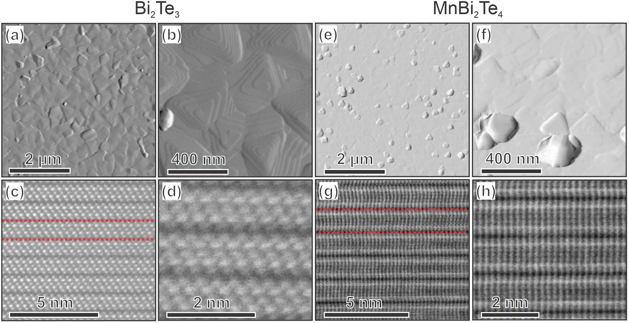 | ||
| Fig. 2 (a and b) AFM surface and (c and d) HRTEM images of Bi2Te3 thin films. The triangular structures with flat terraces and observable steps corresponding to the quintuple layers of Bi2Te3 are clearly shown in (b). (e and f) AFM surface and (g and h) HRTEM images of MnBi2Te4 thin films. MnBi2Te4 exhibits a smoother surface with grains and flat triangle structures. The maximum peak height Sp (which corresponds to the maximum height with respect to the mean height) for AFM images (a), (b), (e), and (f) are 24 nm, 16 nm, 110nm and 75 nm, respectively. The red dotted line corresponds to the (c) Bi2Te3 quintuple layers and (g) MnBi2Te4 septuple layers. | ||
STM and STS measurements were conducted to investigate the surface electronic properties of the Bi2Te3 and MnBi2Te4 thin films. In a typical STS curve, the differential tunneling conductance (dI/dV) is proportional to the local density of states (LDOS) at the STM tip position;26 therefore, it allows us to probe the presence of topological surface states on the MBE grown thin film surface.
A comparison between the LDOS of Bi2Te3 and MnBi2Te4 is presented in Fig. 3. Fig. 3(a) shows a series of dI/dV curves (shaded blue region) taken along a line scan with different positions on the Bi2Te3 surface at room temperature, superposed with the average dI/dV curve (solid blue line). In all measured spectra, the region of positive bias voltage denotes the bulk conduction band (BCB) and the region of negative bias voltage denotes the bulk valence band (BVB), thus confirming a homogenous behavior of Bi2Te3 LDOS throughout the sample surface. The presence of a finite density of states near the Fermi energy (EF = 0) that varies linearly with the bias voltage is a signature of topologically protected surface states, confirming the topological properties of MBE-grown Bi2Te3 thin films.26–29 Moreover, by extrapolating the linear region of the dI/dV curve to the zero conductance axis, it is possible to obtain a Dirac point energy (ED) of −190 meV, which indicates a lightly n-type doping character of Bi2Te3 thin films. Fig. 3(b) shows an averaged dI/dV curve (solid blue line) taken along different points on the MnBi2Te4 surface (blue shaded region). In this case, the topological properties of MBE-grown MnBi2Te4 thin films can be confirmed by the presence of a finite density of states from −0.3 eV to the Fermi level (EF = 0), where the ED is obtained considering the minimum of the dI/dV curve as already been reported in STS measurements in MnBi2Te4 bulk single crystals and thin films.27,30 Because the Bi2Te3 growth parameters are the starting point to obtain MnBi2Te4 with correct stoichiometry, the STS curve indicates that the n-type doping is still present in the MnBi2Te4 phase with the Dirac point located around −210 meV below the Fermi level. Indeed, since at room temperature, antiferromagnetic ordering is not expected to occur, time-reversal symmetry is preserved at the surface of MnBi2Te4, maintaining its topological properties.27 The value for the QL (Bi2Te3) and SL (MnBi2Te4) measured via STM, as shown in the insets of Fig. 3(a) and (b), was 1.01 nm and 1.35 nm, respectively, in agreement with those mentioned previously.
 | ||
| Fig. 3 A series of dI/dV spectra (shaded blue region) and spatially averaged dI/dV curve (solid blue line) obtained along the Bi2Te3 (a) and MnBi2Te4 surface (b). In both graphs, the zero- bias voltage represents the Fermi level (EF) and the red arrow denotes the Dirac point energy (ED). In panel (a), the linear conductance region (dashed red line) indicates the presence of topological surface states (TSSs). Inset shows the STM topographic image where the STS curves were measured, evidencing the QL termination of Bi2Te3 and the SL termination of MnBi2Te4 with step heights of 1.01 and 1.35 nm, respectively. STM images were acquired using I = 400 pA and V = 0.8 V. | ||
To prove the possibility of integrating MnBi2Te4 with group II–VI semiconductors with epitaxial quality, 60 nm thick CdTe was grown on the top of MnBi2Te4 as an insulating cap layer owing to its high resistivity. The HRXRD of this sample is shown in Fig. 4(a). With the exception of the CdTe film reflections known and labeled by CdTe(111) and CdTe(222), all others are identical to those depicted in Fig. 1(f). The film growth aligned with the 00L planes of MnBi2Te4 and showed high crystalline quality. The growth dynamics of the zinc blende crystal CdTe layer on top of the van der Waals material has not been studied; however, it is remarkable that a highly crystalline CdTe layer can be grown onto the MnBi2Te4 film with such a large lattice mismatch. The RSM around CdTe(111) and MnBi2Te4(009) was performed and is shown in Fig. 4(b). The Bragg diffraction peak displays a broader peak in the in-plane direction for the CdTe(111) and MnBi2Te4(009) peaks. The scattering along the crystal truncation rod of CdTe(111) is symmetrical, contrary to MnBi2Te4(009), which is larger for in-plane smaller values.
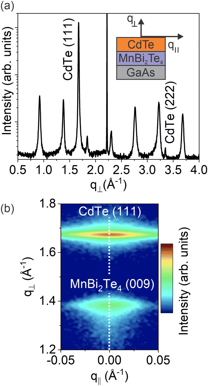 | ||
| Fig. 4 (a) HRXRD and (b) reciprocal map of the GaAs/MnBi2Te4/CdTe heterostructure. | ||
In Fig. 5, we present the results of electrical and magnetotransport measurements for the MnBi2Te4 thin film with a the CdTe cap layer (Fig. 4). As CdTe is highly resistive (usually RCdTe > 100 MΩ), it does not contribute to the measurements. A schematic of the measurement configuration is shown in the inset of Fig. 5(a). Longitudinal electric resistance (Rxx) as a function of temperature is shown in Fig. 5(a), showing the antiferromagnetic transition temperature that manifests as a peak in the Rxx around 19 K. As this value is very close to values reported in the literature for a few SL layers of MnBi2Te4 exfoliated flakes16,25 and for thin films grown via MBE on Si(111),14 it is not clear whether the CdTe cap layer or defects could play some role in the critical temperature of this transition. At low temperatures (<10 K), one observes an increase in Rxx as the temperature is decreased. This is explained by localization effects caused by disorder in the crystal. Moreover, the metallic behavior of the Rxx(T) curve (Fig. 5(a)) shows that electrical transport occurs via the MnBi2T4 layer; otherwise, one would observe a semiconductor-like behavior instead of metallic behavior. Fig. 5(b) shows normalized electrical resistance as a function of temperature for different applied magnetic fields. For clarity, the curves were shifted. The applied magnetic field dislocates the transition to lower temperatures, as expected, because the applied magnetic field tends to suppress antiferromagnetic alignment. It is also possible to observe that the transition is suppressed for B > 3T. Fig. 5(c) presents the transversal electrical resistance (Rxy) as a function of the applied magnetic field. At high temperatures, 20 and 30 K, one observes the linear behavior expected for a single channel transport in this system.31 However, for lower temperatures, 2.1, 6 and 10 K, a dip in the Rxy curves around 3T is clearly observed. In this temperature region, the sample is already in the antiferromagnetic state. The dip in the Rxy curves indicates that for B > 3T, the sample suffers a transition from antiferromagnetic to ferromagnetic.
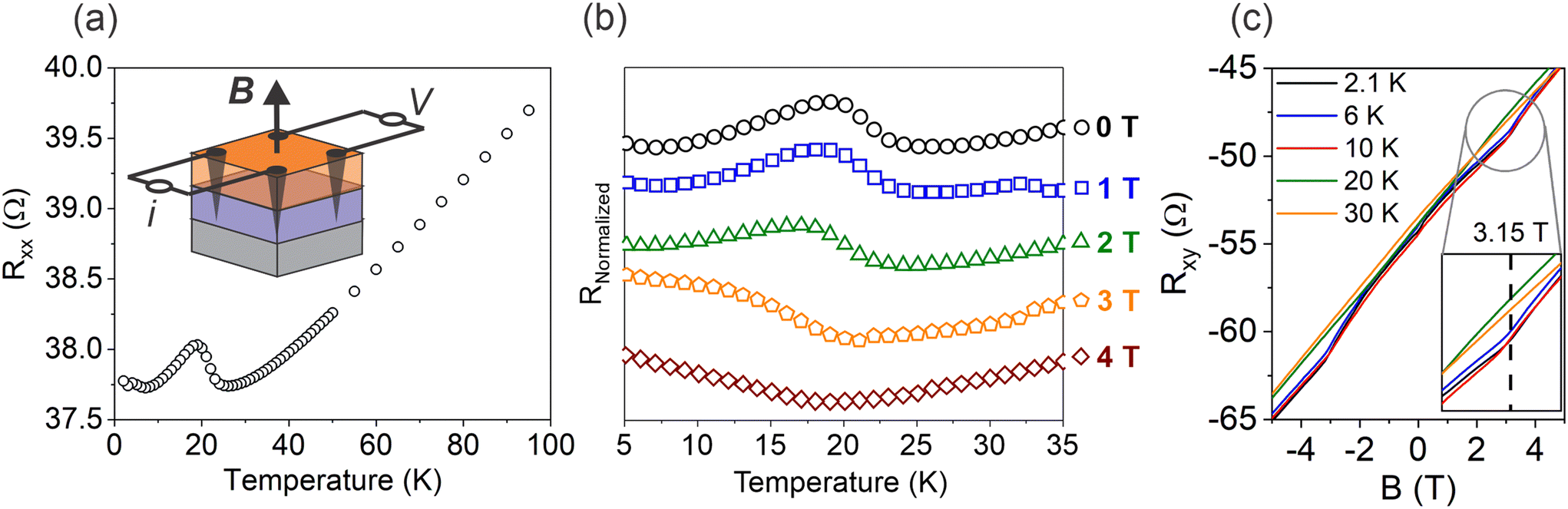 | ||
| Fig. 5 (a) Electrical resistance as a function of temperature, where the AFM transition is clear around 19 K. The inset illustrates the diffusion of indium through the CdTe layer until it reaches the MnBi2T4 film, forming ohmic contact for the measurements. (b) Normalized electrical resistance as a function of temperature for different applied magnetic fields, where it is possible to observe the suppression of the AFM transition for higher fields. (c) The transversal electrical resistence showing a transition from AFM to FM for B > 3T. | ||
Conclusions
In summary, we studied MnBi2Te3 thin layers with topological insulator and ordered magnetic properties. High-quality MnBi2Te3 layers were obtained on GaAs(001) substrates using a recently published Bi2Te3 growth recipe20 by adding only Mn with an effusion cell to achieve the correct MnBi2Te4 stoichiometry. A CdTe layer was used as a cap layer with high epitaxial quality and integration potential with the II–VI semiconductor group through van der Waals growth. Moreover, the metallic behavior of the electrical resistance curve shows that the CdTe cap layer was successfully integrated, thus exhibiting a clean and noise-free signal. GaAs has consolidated industrial fabrication processes and is commonly utilized in existing optical-electronic devices. The integration of MnBi2Te4thin films on the GaAs substrate with II–VI semiconductors establishes a path to intrinsic magnetic topological insulator devices based on the integration between van der Waals materials.Author contributions
Wesley F. Inoch, Sukarno O. Ferreira and Leonarde N. Rodrigues were responsible for the growth of MnBi2Te4via MBE and conducted HRXRD and reciprocal map measurements. Gilberto Rodrigues-Junior and Ângelo Malachias were responsible for STM and STS measurements. S. L. A. Mello carried out AFM measurements. S. de Castro and M. L. Peres carried out transport measurements. Bráulio S. Archanjo, Maybi F. Sampaio and Olavo Teixeira Neto conducted the HRTEM measurements.Data availability
Data are available upon request from the authors.Conflicts of interest
There are no conflicts to declare.Acknowledgements
We acknowledge the financial support by the Brazilian funding agencies CAPES, CNPq (under Grant 408093/2022-6), and FAPEMIG (under Grant APQ-02500-22, APQ-00388-22 and RED-00223-23).References
- M. Z. Hasan and C. L. Kane, Rev. Mod. Phys., 2010, 82, 3045–3067 CAS.
- M. König, S. Wiedmann, C. Brüne, A. Roth, H. Buhmann, L. W. Molenkamp, X.-L. Qi and S.-C. Zhang, Science, 2007, 318, 766–770 Search PubMed.
- O. Breunig and Y. Ando, Nat. Rev. Phys., 2021, 4, 184–193 Search PubMed.
- B. A. Bernevig, C. Felser and H. Beidenkopf, Nature, 2022, 603, 41–51 CAS.
- Y. Tokura, K. Yasuda and A. Tsukazaki, Nat. Rev. Phys., 2019, 1, 126–143 CrossRef.
- Y. Deng, Y. Yu, M. Z. Shi, Z. Guo, Z. Xu, J. Wang, X. H. Chen and Y. Zhang, Science, 2020, 367, 895–900 CrossRef CAS PubMed.
- D. Zhuo, Z.-J. Yan, Z.-T. Sun, L.-J. Zhou, Y.-F. Zhao, R. Zhang, R. Mei, H. Yi, K. Wang, M. H. W. Chan, C.-X. Liu, K. T. Law and C.-Z. Chang, Nat. Commun., 2023, 14, 7596 CrossRef CAS PubMed.
- C.-Z. Chang, J. Zhang, X. Feng, J. Shen, Z. Zhang, M. Guo, K. Li, Y. Ou, P. Wei, L.-L. Wang, Z.-Q. Ji, Y. Feng, S. Ji, X. Chen, J. Jia, X. Dai, Z. Fang, S.-C. Zhang, K. He, Y. Wang, L. Lu, X.-C. Ma and Q.-K. Xue, Science, 2013, 340, 167–170 CAS.
- Q. Li, S.-K. Mo and M. T. Edmonds, Nanoscale, 2024, 16, 14247–14260 CAS.
- M. M. Otrokov, I. P. Rusinov, M. Blanco-Rey, M. Hoffmann, A. Yu Vyazovskaya, S. V. Eremeev, A. Ernst, P. M. Echenique, A. Arnau and E. V. Chulkov, Phys. Rev. Lett., 2019, 122, 107202 CAS.
- Y. Bai, Y. Li, J. Luan, R. Liu, W. Song, Y. Chen, P.-F. Ji, Q. Zhang, F. Meng, B. Tong, L. Li, Y. Jiang, Z. Gao, L. Gu, J. Zhang, Y. Wang, Q.-K. Xue, K. He, Y. Feng and X. Feng, Natl. Sci. Rev., 2023, 11, 1–9 Search PubMed.
- Y. Li, C. Liu, Y. Wang, Z. Lian, S. Li, H. Li, Y. Wu, H.-Z. Lu, J. Zhang and Y. Wang, Sci. Bull., 2023, 68, 1252–1258 CrossRef CAS PubMed.
- P. Kagerer, C. I. Fornari, S. Buchberger, S. L. Morelhão, R. C. Vidal, A. Tcakaev, V. Zabolotnyy, E. Weschke, V. Hinkov, M. Kamp, B. Büchner, A. Isaeva, H. Bentmann and F. Reinert, J. Appl. Phys., 2020, 128, 135303 CrossRef CAS.
- N. Liu, S. Schreyeck, K. M. Fijalkowski, M. Kamp, K. Brunner, C. Gould and L. W. Molenkamp, J. Cryst. Growth, 2022, 591, 126677 CrossRef CAS.
- J. Lapano, L. Nuckols, A. R. Mazza, Y.-Y. Pai, J. Zhang, B. Lawrie, R. G. Moore, G. Eres, H. N. Lee, M.-H. Du, T. Z. Ward, J. S. Lee, W. J. Weber, Y. Zhang and M. Brahlek, Phys. Rev. Mater., 2020, 4, 111201 CrossRef CAS.
- Y.-F. Zhao, L.-J. Zhou, F. Wang, G. Wang, T. Song, D. Ovchinnikov, H. Yi, R. Mei, K. Wang, M. H. W. Chan, C.-X. Liu, X. Xu and C.-Z. Chang, Nano Lett., 2021, 21, 7691–7698 CrossRef CAS PubMed.
- S.-K. Bac, K. Koller, F. Lux, J. Wang, L. Riney, K. Borisiak, W. Powers, M. Zhukovskyi, T. Orlova, M. Dobrowolska, J. K. Furdyna, N. R. Dilley, L. P. Rokhinson, Y. Mokrousov, R. J. McQueeney, O. Heinonen, X. Liu and B. A. Assaf, npj Quantum Mater., 2022, 7, 46 CrossRef CAS.
- A. Koma, Thin Solid Films, 1992, 216, 72–76 CrossRef CAS.
- M. Tanaka, J. Cryst. Growth, 2005, 278, 25–37 Search PubMed.
- L. N. Rodrigues, C. I. L. de Araujo, S. L. A. Mello, J. Laverock, J. M. Fonseca, W. Schwarzacher, W. F. Inoch and S. O. Ferreira, J. Appl. Phys., 2023, 134, 085301 CrossRef CAS.
- A. K. Ray, R. Swan and C. A. Hogarth, J. Non-Cryst. Solids, 1994, 168, 150–156 Search PubMed.
- L. G. Parratt, Phys. Rev., 1954, 95, 359–369 Search PubMed.
- J. Als-Nielsen and D. McMorrow, Elements of Modern X-ray Physics, Wiley, 2011 Search PubMed.
- M. He, Y. Fu, Y. Huang, H. Sun, T. Guo, W. Lin, Y. Zhu, Y. Zhang, Y. Liu, G. Yu and Q. L. He, J. Phys.: Condens. Matter, 2023, 35, 295701 Search PubMed.
- Y. Li, Y. Wang, Z. Lian, H. Li, Z. Gao, L. Xu, H. Wang, R. Lu, L. Li, Y. Feng, J. Zhu, L. Liu, Y. Wang, B. Fu, S. Yang, L. Yang, Y. Wang, T. Xia, C. Liu, S. Jia, Y. Wu, J. Zhang, Y. Wang and C. Liu, Nat. Commun., 2024, 15, 3399 CrossRef CAS PubMed.
- H. Beidenkopf, P. Roushan, J. Seo, L. Gorman, I. Drozdov, Y. S. Hor, R. J. Cava and A. Yazdani, Nat. Phys., 2011, 7, 939–943 Search PubMed.
- H. Kim, M. Liu, L. Frammolino, Y. Li, F. Zhang, W. Lee, C. Dong, Y.-F. Zhao, G.-Y. Chen, P.-J. Hsu, C.-Z. Chang, J. Robinson, J. Yan, X. Li, A. H. MacDonald and C.-K. Shih, ACS Appl. Nano Mater., 2024, 7, 21149–21159 Search PubMed.
- C. Parra, T. H. Rodrigues da Cunha, A. W. Contryman, D. Kong, F. Montero-Silva, P. H. Rezende Gonçalves, D. D. Dos Reis, P. Giraldo-Gallo, R. Segura, F. Olivares, F. Niestemski, Y. Cui, R. Magalhaes-Paniago and H. C. Manoharan, Nano Lett., 2017, 17, 97–103 CrossRef CAS PubMed.
- G. Rodrigues-Junior, T. Chagas, R. Reis, P. V. Sciammarella, C. I. Fornari, P. H. O. Rappl, E. Abramof, R. Magalhães-Paniago and Â. Malachias, Phys. Rev. B, 2023, 108, 035408 CrossRef CAS.
- J.-Q. Yan, Q. Zhang, T. Heitmann, Z. Huang, K. Y. Chen, J.-G. Cheng, W. Wu, D. Vaknin, B. C. Sales and R. J. McQueeney, Phys. Rev. Mater., 2019, 3, 064202 CrossRef CAS.
- J. Cui, M. Shi, H. Wang, F. Yu, T. Wu, X. Luo, J. Ying and X. Chen, Phys. Rev. B, 2019, 99, 155125 CrossRef CAS.
| This journal is © The Royal Society of Chemistry 2025 |