
 Open Access Article
 This Open Access Article is licensed under a
 Creative Commons Attribution 3.0 Unported Licence
Two-dimensional chromium telluride-coated 3D-printed architectures for energy harvesting†
Ritam
Mondal‡
a,
Royston
Mathias‡
a,
Leonardo V.
Bastos‡
b,
Chinmayee Chowde
Gowda
 c,
Nishant
Tiwari
d,
Himanshu
Singh
d,
Cristiano F.
Woellner
b,
Chandra Sekhar
Tiwary
*d and
Partha
Kumbhakar
*a
c,
Nishant
Tiwari
d,
Himanshu
Singh
d,
Cristiano F.
Woellner
b,
Chandra Sekhar
Tiwary
*d and
Partha
Kumbhakar
*a
aDepartment of Physics and Electronics, Christ University, Bangalore 560029, India. E-mail: partha.kumbhakar@christuniversity.in
bPhysics Department, Federal University of Paraná, UFPR, Curitiba, PR 81531-980, Brazil. E-mail: crisfisico@gmail.com
cSchool of Nano Science and Technology, Indian Institute of Technology, Kharagpur, West Bengal 721302, India
dDepartment of Metallurgical and Materials Engineering, Indian Institute of Technology, Kharagpur 721302, West Bengal, India. E-mail: chandra.tiwary@metal.iitkgp.ac.in
First published on 28th April 2025
Abstract
Rapid development of industries, urbanization, and technological advancements have increased demand for sustainable and cost-effective alternative energy sources. In this work, a self-powered flexible 3D-printed triboelectric nanogenerator coated with 2D chromium telluride (Cr2Te3) (3D-TENG) is presented as an innovative energy harvesting approach from pressure and temperature. The optimized flexible 3D-printed hexagonal structures with coatings show varying specific yield strength and porosity. The 3D-TENGs achieved a maximum output voltage of ∼39 V under periodic impacts of ~0.8 kPa and their performance further increased (∼45 V) in the presence of varied temperatures. The outstanding results and flexibility of the 3D-TENG devices highlight their potential in self-powered energy harvesting from external heat, magnetic fields, and body weight. Density functional theory (DFT) calculations further explained the interaction between 2D Cr2Te3 and the polymer surface under external impact. Therefore, we believe that our findings illustrate the potential of integrating 2D materials with 3D-printed architectures to enhance the efficiency and adaptability of flexible, lightweight, low-cost, and eco-friendly TENG devices for industrial applications.
1. Introduction
One of the major problems of the 21st century is the ever-increasing need for energy. The world's power consumption is rising exponentially due to factors such as fast industrialization, urbanization, and increasing dependence on electronic devices.1 In response to economic and environmental pressure associated with non-renewable fossil fuels, global energy generation has undergone a significant transformation.2 Renewable energy sources, including geothermal, hydro, wind, and solar power, are being integrated increasingly into the energy grid.3 These technologies harvest electricity by using naturally occurring processes, thereby eliminating problems such as greenhouse gas emissions,4 depleting natural resources, and dependency on finite fossil fuels.5 A lot of advanced research involves conversion of ambient energy from the environment into usable electricity. Among these, triboelectric energy generation has emerged as a particularly promising technology.6 TENGs offer a flexible and environmentally friendly energy generation method that complies with the values of conservation and sustainability. TENGs are promising as they efficiently transfer mechanical energy, which can come from human motion, vibrations, and even wind, into electrical energy that can be used for various purposes. Recently, self-powered TENGs have received great attention.7 Triboelectricity is a surface-dependent phenomenon driven by charge transfer at material interfaces.8 Therefore, the magnitude of the charges and the surface properties of interacting materials are the two critical factors that determine the amount of output voltage generated.2D materials present a path to enhance the power output of TENGs.9 Strong covalent bonds give 2D materials their in-plane stability, whereas van der Waals forces enable a comparatively weak interlayer attraction that permits the exfoliation of the bulk material into discrete, atomically thin layers. These 2D materials of atomic size thickness have unique properties such as a large specific surface area, ease of surface modulation and exceptional electrical conductivity,10,11 offering advantages in terms of surface charge generation. 2D materials such as graphene and its derivatives12 and hexagonal boron nitride (h-BN)13 have a wide bandgap and low electron affinity, thus making them tribo-positive materials. In contrast, materials such as graphene, molybdenum disulfide (MoS2), and transition metal dichalcogenides (TMDs)14,15 have high electron mobility and strong electron affinity, making them tribo-negative materials.16,17 When utilized as bare materials, these materials exhibit weak adhesion, fragility, high sensitivity to environmental conditions, etc., even though they are good candidates for TENG applications. Furthermore, a wide range of reported TENG devices utilize polymer thin films or cellulose substrates that are prone to wear and tear. To eliminate these effects and to improve energy generation via contact electrification and electrostatic induction, the surface morphology of triboelectric polymers in TENGs has recently been modified through micro- and nanopatterning.18 However, to create less expensive nanopatterns, more effective techniques are being sought. Thus, 3D printing offers the advantages of being mechanically stable, flexible, affordable, effective, long-lasting, and environmentally friendly.19–22 Complex TENG devices have shown considerable promise for development using 3D printing technology. 3D-printed TENGs have been largely utilized because of their sustainability, affordability, ease of fabrication, and complex architectures.23–25
Here, we have reported 2D Cr2Te3-coated 3D-printed hexagonal structures with varying porosities that are utilized as energy harvesting systems from mechanical impact and temperature. We have printed the structures using the effective fused deposition modeling (FDM)20 technique. We have demonstrated the hexagonal structure of 3D-printed devices, which enhances their compression resistance, reducing wear and tear over time. This increased durability contributes to long-term reliability, making 3D-printed TENGs more advantageous compared to traditional polymer-based or cellulose-based counterparts. The primary benefit of employing intricately shaped 3D-printed structures is that their increased surface area allows for larger surfaces for coating 2D materials, aiding in the production of high-output voltages. The mechanical strength and durability of 3D-printed structures ensure the lengthy lifespan of the manufactured device. The 3D-TENGs produced an output voltage, which further increased with a rise in temperature by illumination with infrared light. The fabricated and coated device was used in various applications to generate energy for our daily life.
2. Materials and methods
2.1 The fabrication of 2D Cr2Te3
To fabricate 2D Cr2Te3, stoichiometric amounts of pristine high-purity chromium (Cr) and tellurium (Te) chunks (99 wt%) served as the base materials for producing a Cr–Te alloy. The fact that the two elements’ melting temperatures differ significantly, Cr (∼1907 °C) having a melting point much higher than Te (∼450 °C), both components were sealed in a quartz tube before melting. To prevent the oxidation of Te, which is very volatile at higher temperatures,26 an inert atmosphere was created using argon (Ar) gas that was backfilled into the quartz tube. After that, the alloy was melted in an induction furnace at 1350 °C and the temperature was maintained for two hours. Following the melting phase, the samples were subjected to an extended heat treatment at 900 °C for a duration of 75–80 hours. This was done to achieve homogeneity of the alloy. This forms a bulk Cr2Te3 alloy.The bulk Cr2Te3 was cut into small chunks, physically crushed, and powdered with a mortar and pestle. The powders were then dispersed in isopropyl alcohol (IPA) solution. The sample-to-solvent ratio was maintained at 1 g![[thin space (1/6-em)]](https://www.rsc.org/images/entities/char_2009.gif) :10 ml. The solution was exfoliated for 4 hours using a 10-second pulse-rate probe sonicator operating at 30 kHz. The exfoliated solution was allowed to stand for a few hours, so the larger particles settled down and well-dispersed Cr2Te3 nanosheets were obtained.
:10 ml. The solution was exfoliated for 4 hours using a 10-second pulse-rate probe sonicator operating at 30 kHz. The exfoliated solution was allowed to stand for a few hours, so the larger particles settled down and well-dispersed Cr2Te3 nanosheets were obtained.
2.2 Fabrication of the flexible 3D-TENG and coating with 2D Cr2Te3
3D printing was performed using fused deposition modeling (FDM) (Flashforge Creator Pro) (Fig. 1). Complex structures can be printed using this technique using a thermoplastic polyurethane filament. This is a typical additive manufacturing (AM) process that involves heating the filament and forcing it through a nozzle to form layers. Every layer's pattern is determined by the nozzle's x–y location. Next, as it advances along the build plate, the print head deposits each layer one after the other. We used a TPU filament of 1.75 mm diameter that has a print temperature of 200–220 °C. The filament was loaded into the printer, where the rollers guide the filament into the heated extruder nozzle. The printing was conducted using the left extruder, with a diameter of 0.4 mm at a temperature of 230 °C and the bed temperature was 50 °C. The printer was set to standard mode. The printing instructions were provided using the printer slicer software Flash Print-5. The dimensions of the structure were 15 mm × 13 mm × 15 mm and 30% and 40% infills (H1 and H2 structures, respectively) were selected using the Slicer software itself. The printing parameters such as printing speed, raft enable and other parameters were set and then fed into the printer. After the 3D structure was ready, the raft was removed and the structure was prepared for coating. | ||
| Fig. 1 (a) Atomistic model of Cr2Te3 and (b) surface interaction with a TPU monomer. (c) X-ray diffraction patterns of bulk Cr2Te3 and 2D Cr2Te3, (d) Raman spectra of 2D Cr2Te3, (e) TEM image of 2D Cr2Te3, and (e-I) and (e-II) FFT pattern and line spacing of exfoliated Cr2Te3. (f) Schematic of 3D printing the hexagonal structures, dip-coating with 2D Cr2Te3 and fabrication of the TENG device, (g and h) optical image of the 3D structure, (i) SEM images of 2D Cr2Te3 coated on the TPU structures and (j) 3D structures with varied layers of 2D coating of Cr2Te3. | ||
The printed structures were initially submerged in the exfoliated liquid for a duration of 24 hours. Following this, the structures were subjected to a drying process in a hot oven maintained at 70 °C for 5 hours to ensure complete removal of residual solvent (IPA) (Fig. 1e and f). Hence, 2D Cr2Te3-coated H1 and H2 structures for the device fabrication were obtained (Fig. 1d). One of the flat surfaces of each structure was attached with Kapton tape, which functions as a neutral material essential for the operation of the TENGs. Subsequently, copper tape was attached to both flat surfaces of the structure, serving as external contacts to facilitate the measurement of the electrical output (Fig. 1d). Furthermore, the structure was coated multiple times, as shown in Fig. 1h, and tested for voltage generation under IR light and varying temperature conditions.
2.3 Characterization
Scanning electron microscopy was conducted using a Thermo Fischer Apreo S LoVac to confirm the coating morphology of Cr2Te3 on TPU. X-ray diffraction patterns were collected and crystalline phase information was obtained using an X-ray diffractometer (Bruker D8 Advance) with a Cu-Kα source operating at 40 kV voltage and 40 mA current with a wavelength (λ) of 1.5406 Å. High-resolution transmission electron microscopy (HRTEM) was conducted using a JEOL F30 FEI machine running at 300 kV to investigate the microstructural properties of the samples. For optimal imaging, the samples were first exfoliated and then dispersed in ethanol, ensuring that the particles were evenly distributed throughout the solution. The sample dispersion was sonicated for ten minutes and then one or two drops of the prepared sample were carefully drop-cast onto a copper grid for imaging. The copper grid, which was coated with holey carbon, featured a 500 square mesh specification, allowing for fine imaging and stabilization of the sample under the electron beam. The material's chemical characteristics and vibrational modes were studied by Raman spectroscopy using a WITec Raman spectrometer (WITech, UHTS 300 VIS, Germany) operated at a 532 nm laser excitation wavelength, which was carried out at room temperature (RT). Furthermore, X-ray photoelectron spectroscopy (XPS) was performed using Al-Kα radiation (λ = 1486.71 eV) as the X-ray source. Measurements of voltage were made with a DSO Textronix 1072B. The zeta potential and particle size were measured using a Litesizer 500 (Anton Paar).2.4 Computational analysis of contact electrification
To support our experimental findings and to reinforce them with a more detailed description, we also designed an atomistic model for contact electrification between Cr2Te3 and TPU surfaces and performed first-principles calculations using density functional theory (DFT). Based on a Cr2Te3 unit cell, we first constructed a 2 × 5 × 1 supercell. To simulate the two-dimensional nature of the exfoliated material, the supercell was cleaved along the (001) plane and a vacuum layer of 20 Å was added above the resultant surface. The purpose of this vacuum is to avoid periodic interactions in the direction perpendicular to the surface while maintaining periodic boundary conditions in parallel directions. Using this configuration, which is shown in Fig. 1a and b, we computed the work function. The work function indicates how well charge may be created through contact electrification. It is the least energy required to remove an electron from the surface of a material.27 The energy difference between the Fermi energy level and the electrostatic potential value under vacuum far from the surface was calculated to determine it.The approximation for the exchange–correlation energy utilized in all calculations was the Perdew–Burke–Ernzerhof (PBE)28 functional, as implemented using the CASTEP tool. The OTFG ultrasoft pseudopotential with an energy cutoff of 381.00 eV was used to describe the interaction between core and valence electrons. To obtain the electrostatic potential, geometry optimization was performed until an energy variation of less than 10−5 eV was verified between steps. The work function was then obtained by taking the difference between the average value of the electrostatic potential at a plane parallel to the surface, located inside the vacuum region, and the Fermi energy obtained through the calculation.
Following this process, a TPU unit cell was introduced to the vacuum layer parallel to the Cr2Te3 surface to simulate the contact electrification process, as illustrated in Fig. 1a and b. This unit cell is representative of the hard parts present in TPUs, which can be modeled in a crystalline pattern. In the model we used,29 the urethane bonds are composed of diphenylmethane 4,40-diisocyanate (MDI) molecules and 1,4-butanediol (BDO), which is used as a chain extender. With the goal of identifying interfacial charge transfer, we then performed a single-point energy calculation and obtained the electron localization function (ELF) and the charge density distribution. The ELF provides a visual way to quickly convey chemical bond information, as it allows us to differentiate between covalent, single, double, and triple bonds30 and the electron density plot allows us to identify charge transfer between the surfaces.
3. Results and discussion
3.1 Structural and morphological properties of 2D Cr2Te3-coated 3D structures
The bulk Cr–Te alloy was synthesized through induction melting at 1350 °C, ensuring a high degree of alloying and homogeneity. The phase formation of the resulting alloy was confirmed through X-ray diffraction (XRD) analysis (Fig. 1c), which provided clear evidence of successful alloying. Following this, the bulk samples were mechanically crushed and exfoliated using a probe sonication technique for 10 to 12 hours. This sonication process facilitated the exfoliation of the bulk material into thinner layers, which were then suspended for 48 hours to further separate any larger particles. Post-suspension, the samples were centrifuged to remove any remaining impurities and then dried and collected for other characterization studies. The exfoliated 2D structure of Cr2Te3 was made based on the bulk prototype, where van der Waals (vdW) layers were found to lie predominantly in the (100) crystallographic plane. This plane, with an interlayer distance of approximately ∼3 Å, was identified as the primary plane of exfoliation. The structure of these 2D layers consists of Cr4Te16 units, which are composed of four edge-sharing CrTe6 octahedra. These octahedra form a continuous 2D layer structure by connecting at the corners with nearby Cr4Te16 units. Visual confirmation of this 2D structure was modeled based on the Cr-centered polyhedral arrangement, depicted in the inset of Fig. 1c, which provides a clear representation of the Cr2Te3 structure. The most highly exfoliated planes were experimentally confirmed using XRD analysis of exfoliated Cr2Te3 to be (100) planes. Raman spectroscopy was employed to understand the vibrational characteristics of the material. The spectrum exhibits four different peaks at Raman shifts of 96.06 cm−1, 101.18 cm−1, 119.56 cm−1 and 137.04 cm−1, which show different vibrational modes. The peak at 119.56 cm−1 shows the most dominant and functional vibrational mode inside the structure. Moderate intensity peaks at 96.06 cm−1 and 101.81 cm−1 indicate the presence of significant phonon modes with a lower peak at 137.07 cm−1 (Fig. 1d). Using X-ray photoelectron spectroscopy (XPS), the composition of the exfoliated 2D Cr2Te3 sample was verified through a survey scan (Fig. S1†). The XPS analysis revealed distinct peaks corresponding to both chromium (Cr) and tellurium (Te) elements, validating the successful formation of the Cr2Te3 composition. Specifically, the Te 3d and Cr 2p core level spectra provided clear indications of surface oxidation, as evidenced by the presence of oxidation peaks. However, due to the overlap of the Te 3d signals with the Cr 2p core level, deconvoluting the peaks posed certain challenges, introducing a degree of uncertainty in quantifying the oxidation states of Cr and Te. Therefore, the results should be considered as estimates rather than definitive values. The Cr 2p core level spectra are shown in Fig. S2a,† where characteristic satellite peaks appear at 574 eV and 584 eV. Additionally, the main peaks of Cr 2p are observed at 577 eV for the 2p3/2 state and 586 eV for the 2p1/2 state with full width at half maximum (FWHM) values of ∼3.1 eV and ∼3.5 eV, respectively, indicating the Cr oxidation states. Similarly, the Te 3d peaks are depicted in Fig. S2b,† with a peak at 577.35 eV for the 3d1/2 state, which overlaps with the Cr 2p3/2 peak. Additionally, the Te 3d5/2 peak shows significant overlap, complicating the precise deconvolution of these signals. Despite these overlaps, the overall spectra affirm the presence of both elements in the Cr2Te3 structure. Furthermore, the work function of exfoliated Cr2Te3 was determined using the XPS data and was calculated to be ∼3.522 eV (Fig. S3†). The exfoliated sample was then subjected to particle size analysis using a Litesizer 500 (Anton Paar), where the average lateral size of 2D Cr2Te3 was found out to be ∼1.8 μm (Fig. S4†). The sample dispersion was drop-cast onto a 500-mesh holey carbon grid for additional morphological examination. The HRTEM image of a Cr2Te3 flake with an FFT pattern is shown in Fig. 1e. The monoclinic pattern stacking is visible in the FFT pattern. Based on Fig. 1e(I), the line profile shows a spacing of approximately 128 pm, which corresponds to the atomic radii of Te atoms. In the (110) plane, the fringes are roughly spaced at d = 0.206 nm. Furthermore, the HRTEM image (Fig. S5†) was used to observe the edge defects present in the exfoliated Cr2Te3, which contribute to the overall charge generation during the TENG operation. The coating of Cr2Te3 was confirmed by SEM images, which show the morphological and structural information of the coated Cr2Te3, as shown in Fig. 1e(II). From the figure, we can see the rough sheet-like structures and flaky appearance of the material in the range of ∼1 μm or larger, indicating textures that are commonly found in 2D materials or nanostructured compounds. Finally, we confirmed the presence of Cr and Te in the bulk and exfoliated samples using Electron Diffraction Spectroscopy (EDS) (Fig. S6†).3.2 Mechanical property analysis of the 3D-printed hexagonal structure
The load-bearing capacity of the structures was measured along the perpendicular direction of the layer printing direction through the compression testing of the 3D-TENGs using a UTM Instron 3365. The two distinct pristine 3D-printed structures H1 and H2 with dimensions of 15 mm × 13 mm × 15 mm and densities of 0.598 g cm−3 and 0.786 g cm−3, respectively, were used. The surface area/volume ratio and porosity are the essential variables for the design of distinct architectural porous structures. Among these structures, H2 has less porosity but a higher surface area/volume ratio compared to the H1 structure. Throughout the compression tests, a continuous strain of 1 mm min−1 was applied. An optical camera was used in front of the testing setup to analyze the deformation behavior of the structures. Mechanical properties such as Young's modulus, specific compressive strength (yield strength of the structure/density), and specific resilience (area under the curve up to the elastic region of the structure/density) were calculated for investigating the structural performance of the 3D-printed structures. Initially, the stress distribution for the hexagonal structures was analyzed. The amount of deformation for H1 and H2 was calculated at different strain percentages (∼0%, 10%, 20%, 30%, 40%, 50%, and 60%), as shown in Fig. 2(a and b). The compression test data were analyzed and the geometrical and mechanical representation values are presented in Tables S1 and S2.† Ultimate strength is the highest point on the stress–strain curve, representing the peak load-bearing capacity of the material.31 Beyond this point, the structure typically experiences irreversible deformation or failure. The ultimate strength of H1 was 0.31 MPa, while the ultimate strength of H2 was 0.62 MPa, as shown in Fig. 2d and Fig. S7 and S8.† The higher ultimate strength of H2 indicates a better load-carrying capacity, making it more suitable for applications requiring high strength. The deformation of H1 showed a gradual increase in strain, indicating a higher stress distribution across the structure (Fig. 2c). At higher strain percentages, H1 exhibited larger deformations, suggesting that it can tolerate more strain before failure. Furthermore, we have calculated the Young's modulus (Fig. S9 and S10†) that measures the stiffness of a material. Here, H1 shows a lower Young's modulus of 0.119 MPa, while H2 shows a higher Young's modulus of 0.359 MPa (Fig. 2h), indicating that H1 has greater flexibility, which is perfect for applications such as triboelectric devices where flexibility plays an important role in enhancing the performance. Furthermore, the specific yield strength was also calculated and it is defined as the compressive strength of a composite material divided by its density. This measure allows for comparison of materials with different densities, highlighting the strength-to-weight ratio. The specific yield strength for the H1 structure is 0.0059 MPa g−1 cm−3 and that of the H2 structure is 0.0233 MPa g−1 cm−3, as shown in Fig. 2i, which shows a 132% increase in yield strength when porosity was decreased by ∼20%. The specific resilience of the structure is also defined as the area under the stress–strain graph until the elastic region, divided by its density, and the calculated specific resilience for the H1 structure was found to be ∼0.0035 MPa g−1 cm−3 and that for the H2 structure was found to be ∼0.0738 MPa g−1 cm−3 (Fig. S11 and S12†). The specific compressive strength and specific resilience were higher for H2 (about 20 times that of H1), consistent with its lower porosity and higher density (Fig. 2e and g). These properties indicate that H2 can absorb more energy per unit density (specific resilience) before deformation and has a better strength-to-weight ratio compared to the H1 structure (Fig. 2f). After removing the load, the deformed structure starts regaining its original shape (Fig. S13†). In triboelectric devices, flexibility plays a crucial role in generating electrical signals. In such devices, the materials must deform easily under mechanical stress to maximize surface contact and separation, which enhances the triboelectric effect. The flexibility of a material allows it to adapt to varying mechanical inputs, leading to more efficient energy conversion. Here, the flexibility, higher surface area per unit volume (Fig. 2j) and adequate mechanical properties of the H1 structure make it an ideal structure for various low-load applications. | ||
| Fig. 2 (a and b) Deformation of the 3CTH1 and 3CHT2 structures when an external pressure is applied, (c) stress–strain plot of the 3CTH1 and 3CTH2 structures, (d) compressive load–compressive extension curve of the 3CTH1 and 3CTH2 structures, (e) comparison of the porosity of the 3CTH1 and 3CTH2 structures, (f) comparison of the volume of the 3CTH1 and 3CTH2 structures, (g) comparison of the density of the 3CTH1 and 3CTH2 structures, (h) comparison of the Young's modulus of the 3CTH1 and 3CTH2 structures, (i) comparison of the specific yield strength of the 3CTH1 and 3CTH2 structures and (j) comparison of the surface area/volume of the 3CTH1 and 3CTH2 structures. | ||
3.3 Measuring the voltage output of the 3D-TENGs
The TENG device was fabricated by connecting the electrodes to the coated 3D-printed structure. One of the flat surfaces of each structure was attached with Kapton tape as a triboelectric layer. Subsequently, a metal electrode (copper tape) was attached to both surfaces of the structure, serving as contacts, as seen in Fig. 3a (see the Experimental section for more details). The output was measured at varied impacts and frequencies. The tapping frequency was 3 Hz (periodic taps) (ESI video S1†). The output performance was calculated from the voltage density (JVoc) graph, which is voltage per unit area, as shown in Fig. 3(b and c). In Fig. 3(d and e), we present the output voltage as a function of pressure and the maximum output voltage was found to be ∼38 V for the H1 structure and ∼39 V for the H2 structure under a mechanical impact of 900 Pa. Additionally, we charged a 100 μF capacitor using the output voltage of 3D TENGs, which showed the charging and discharging cycles of the capacitor (Fig. 3f). The charging and discharging times of the capacitor are almost symmetric with a time constant (τ) value of ∼1.45 s. Furthermore, we have measured the internal resistance (RL) of the fabricated device by connecting a circuit, as shown in the inset of Fig. 3g. It was found that the RL of the device was ∼20 MΩ with a current rating of ∼1 μA (Fig. 3g), from which we calculated the power output from the device and it was found to be ∼20 μW. Therefore, the fabricated 3D-TENG system can be used to power a small electronic device under mechanical impact. Furthermore, to confirm that the 3D-printed structures are advantageous for better output voltage, a cellulose paper substrate was coated with Cr2Te3 and its output voltage was compared with those of the H1 and H2 TENG devices. As shown in Fig. S14,† the comparison showed that the 3D printed structures gave considerably better output than the paper-coated TENG device. This also confirms that the increased specific surface area provided by the 3D-printed structures aids in achieving higher output voltage (see the ESI for more details†). | ||
| Fig. 3 (a) Experimental setup and schematic diagram to measure the output voltage of the TENG devices at different applied pressures, (b and c) voltage density vs. time plot of the CTH1 and 3CTH2 structures at 1.2 N force and a temperature of 60 °C, (d and e) output voltage measured at various applied external pressures, and (f) charging and discharging cycle for an external capacitor. (g) Voltage vs. resistance (log axis) curve of the TENG device. The inset shows the circuit used to measure the internal resistance of the TENG device. (h) Schematic diagram of different stages of contact-triboelectrification. (i) The 2D layer and TPU are in contact due to external pressure, (ii) the 2D layer and TPU start to separate when the external pressure is released, (iii) the 2D layer and TPU are completely separated when the external pressure is removed, and (iv) the 2D layer and TPU are approaching again due to the external pressure. | ||
The 3D-TENG device was designed by using the common contact separation mode using Cr2Te3 as the tribo-positive layer with the most common charges of +3 and +6 and TPU as the tribo-negative layer. The principle of operating the 3D-TENG is illustrated schematically in Fig. 3h, which shows how electrons are transferred in a contact separation mode. When a periodic external pressure is applied (Fig. 3h-i), the positive 2D material initially comes in contact with the negative TPU. Both materials’ surfaces generated positive and negative charges, respectively, with no electron transfer occurring. Furthermore, when the external pressure is removed (Fig. 3h-ii), both the surfaces are separated and a space is formed in between, which produces an electric potential difference and the electrons are transferred from one electrode to another via an external load, and hence an electrical current is produced. Once the separation between the two surfaces reaches the maximum (Fig. 3h-iii), due to the electrostatic equilibrium, the electron flow is stopped. When the external force is applied again, it disturbs the electrostatic equilibrium, and a new opposing potential difference is produced and the electron current starts to flow in an opposite direction (Fig. 3h-iv). Alternating current is produced because of continuous electron flow between the top and bottom electrodes throughout the contact separation process.32
The output voltage generated by the 3D-TENG is given by the following equation:33
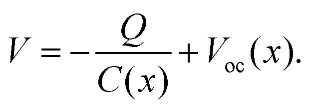 | (1) |
This equation is known as the V–Q–x relationship, which represents the innate capacitive behavior of the TENG, where Voc is the open-circuit voltage, C(x) is the capacitance between two electrodes, and Q is the charge transferred between two electrodes.
3.4 Computational analysis for triboelectrification
To determine the interaction between atomically thin Cr2Te3 and the surface of TPU under mechanical impact, DFT calculations were carried out further. The electrostatic potential variation in the direction perpendicular to the surface of Cr2Te3 is shown in Fig. 4. The assigned numerical value is the average potential at a plane parallel to the surface. By subtracting the vacuum and Fermi energies, we determined the work function to be 3.618 eV, which closely matches the value of ∼3.522 eV found experimentally, which is lower than those of most metals. For comparison, gold has a work function of about 5.1 eV, while both silver and copper have values of around 4.7 eV. As less energy is required to remove an electron from the Cr2Te3 surface, this material is expected to act as a tribo-positive component when paired with TPU. In Fig. 4a–d, we show the electron localization function and the charge density calculations. The electron localization function assigns a 0 to 1 value to the probability of finding an electron in proximity with a reference electron of the same spin. Values close to 1 represent a very localized ELF and indicate strongly bound electrons, often associated with covalent bonds or the existence of stable electron pairs, while 0 denotes the total absence of electrons. An ELF value of 0.5 is generally indicative of metallic bonds and is the characteristic value for an electron gas. The Cr2Te3 surface atoms, which are all chromium, show a somewhat non-localized ELF even before the introduction of the TPU layer into the system, as can be seen in Fig. 4a and b where the ELF reaches a maximum value of around 0.7. For comparison, Fig. 4b (lower panel) shows the same calculation for the layer of tellurium atoms below the surface, where a strong localization is present and distinct shells can be clearly seen. The non-localization at the surface suggests that electrons are weakly bound to the chromium atoms and the ELF values close to 0.5 (depicted by the green regions) indicate the presence of free electrons. This abundance of free charges contributes to the amount of charge generated through the triboelectric effect. To highlight the presence of negative charges on the surface, we have also conducted a Mulliken population analysis. Even though the absolute values of charge are known to be sensitive to the atomic basis set used for the calculation, this method can be very useful for identifying qualitative variations in a system, such as changes in electron density. For the system containing only Cr2Te3, we obtained a surface charge density of −1.182 × 10⁻² C m−2, meaning that the chromium atoms are negatively charged and electrons accumulate at the surface. If charge transfer occurs upon interaction with the TPU surface, this value is expected to shift, becoming more positive if electrons flow from the surface to the TPU, and more negative otherwise. With the addition of the TPU molecule, more green regions (representing an ELF of 0.5) start to appear, as shown in Fig. 4e. This shift indicates that electrons are being removed from the surface and thus gained by the TPU molecule. This transfer is corroborated by the new Cr2Te3 surface density of 7.571 × 10⁻² C m−2, becoming positively charged, and by the charge density distribution shown in Fig. 4e, where the presence of electrons can be seen in the previously empty vacuum region. Considering its low work function and the abundance of free surface charge, our theoretical results show that Cr2Te3 is a viable option to be used as the tribo-positive component of a triboelectric nanogenerator. Paired with TPU as the tribo-negative part, we achieve an effective combination for the generation of charge via contact electrification. | ||
| Fig. 4 (a and b) Electron localization function calculated for the chromium atoms at the Cr2Te3 surface (green cross section) and for the tellurium atoms below the surface (red cross section) before and after contact with TPU, (c and d) Mulliken charge distribution before and after contact with TPU, and (e) average value of the electrostatic potential inside the simulation cell in the direction perpendicular to the surface. The Fermi and vacuum levels indicated were used for the calculation of the work function. | ||
3.5 The output performance of 3D-TENGs under temperature, magnetic field, and weight conditions
Furthermore, we have measured output voltage under a wide range of temperature conditions (Fig. 5a and Fig. S15, S16†) (starting from room temperature to higher temperature ranging from 25 °C to 70 °C) and we observed a trend of increase in the output voltage as the applied temperature was increased. From Fig. 5b, the maximum output voltage for each structure was observed at ∼60 °C, which was ∼45 V for H1 and ∼39 V for H2. Therefore, these results conclude that our 3D-TENG devices could work optimally when the applied external pressure was ∼900 Pa and until a temperature of ∼60 °C. The increase in voltage is attributed to the charge generated due to the temperature gradient in the sample, as schematically shown in Fig. 5c. To probe the temperature gradient in the coated structure, the IR-thermal imaging method was used to confirm it. As we can see from Fig. 5d, the heat at the bottom surface (where the heating element is nearer) of the sample increases rapidly compared to the top surface. This generates an increasing temperature gradient concerning time, as shown in Fig. 5e. The variation of output voltage with temperature was further verified with a classical electrodynamics model as discussed below. The electronic thermionic emission is given by the following equations:| σ = −C1Th + C2 | (2) |
| σtc = e−SAt0σtc0 | (3) |
 | (4) |
| Sensitivity = ΔVo/Δm | (5) |
| FOM = Sm = dVo/Vo | (6) |
 | ||
| Fig. 5 (a) Curve showing the increase in the output voltage with increasing temperature plotted in terms of voltage density vs. time, (b) output voltage measured at various temperatures at an applied pressure of 900 N m−2, (c) schematic of creating a temperature gradient in the TENG device, (d) IR images of the TENG devices, which show a temperature gradient at different time intervals, and (e) temperature gradient vs. time curve of the TENG device. | ||
Hotter bodies, such as electronic gadgets and home appliances, generally emit IR radiation. The human body also emits infrared (IR) radiation as a part of body heat, ranging from 40 to 57 W m−2, due to metabolic activities. Therefore, the detection of IR emission from different sources is of urgent need. As observed earlier, 3D-TENGs show good response under external temperature conditions. We have studied the effect of IR light on the device. IR light is electromagnetic radiation with longer wavelengths than the visible region yet shorter compared to microwaves, ranging from 700 to 1000 nm wavelengths. A setup was made using an IR lamp of 700–1200 nm wavelengths and placed in front of the 3D-TENG device (Fig. 6a), where the irradiated light intensity was changed from 1 to 40 W m−2 (Fig. 6a-I). A constant pressure of 0.15 MPa was applied to the device and the variation of the output voltage of the device concerning the change of IR intensity is shown in Fig. 6a-II. It was observed that the irradiated IR light increased the output voltage from ∼0.47 V to 1.02 V. It was found from the plot (Fig. 6a-II) that in the lower intensity range of the IR lamp of 1–10 W m−2, the output voltage generated had a sensitivity of ∼44 mV m2 W−1 and in the higher intensity range of the IR lamp (10 to 40 W m−2), sensitivity dropped to 3 mV m2 W−1. Additionally, the variation of FOM was also calculated for the change in the irradiated intensity of IR. The FOM ranged from 0.3 to 0.08 with the increase of irradiated intensity from 1040 W m−2. These results show that the IR radiation helps in enhancing the energy harvesting nature of the fabricated device. The IR rays interact with the material and contribute to energy generation by increasing the temperature.
 | ||
| Fig. 6 (a) Experimental setup to measure the output voltage at different IR radiation intensities, (a-I) IR images of the TENG devices when irradiated with IR light at various intensities, (a-II) output voltage vs. the intensity of IR light curve, (b) schematic of the 3CTH structure under a magnetic field, (b-I) experimental setup to find the output voltage when the magnetic field is applied from only one side, (b-II) experimental setup to find the output voltage when the magnetic field is applied from both sides, (b-III) curve to compare the output voltage when a magnetic field is applied from one side and both sides at different applied magnetic fields, (c) schematic diagram showing the application of the 3CTH TENG device as a mass measuring instrument, (c-I) experimental setup showing the sensing of human body mass as a function of voltage and (c-II) curve of voltage vs. weight applied. | ||
2D Cr2Te3 is known to have good ferromagnetic properties, as shown in Fig. S22,† and thus with an expectation of sensing an external magnetic field, we tested our device under a magnetic field (Fig. 6b). A constant pressure of 0.15 MPa was applied to the device and different measurements of output voltages under different magnetic fields varying from 0 to 64 mT were performed. The magnets were first aligned on one side and then on both sides to check the variation (Fig. 6b-I and II). It was observed that the applied magnetic field (0 to ∼64 mT) increased the output voltage from 0.36 V to 0.51 V (for one side alignment) and from 0.29 V to 0.44 V (for both side alignment) (Fig. 6b-III).
From the analysis of the triboelectric behavior of our structure coated with Cr2Te3 and the promising results, it can be used as a device for weight sensing under varying weights and pressures (Fig. 6c). As the 3D-printed structures show very good mechanical properties under loading conditions, we have further used the structures as weight sensors. The weight-sensing performance of our structure can be investigated using output voltage at different weights (weight in kg). In our case, we selected five people of different weights ranging from 45 to 70 kg and made them stand on our device, as shown in Fig. 6c-I. ESI Video S2† illustrates the output voltage's corresponding reaction when a 60 kg human stands on the device. Fig. 6c-II plots and illustrates the variation in the average output voltage of the devices under varying human weights. The output voltage and weight graph has been linearly fitted and it has been noted that a person's weight increases the output voltage. The slope of the output voltage vs. weight graph provides insight into the voltage generated per unit change in weight (in kg). It was found that there is an increase in output voltage with a sensitivity value of ∼6.4 mV kg−1. Additionally, the variation of the FOM concerning weight has been calculated for different changes in output voltage with corresponding weights. The values of FOM varied from 0.17 to 0.03 with the increase of weights from 45 to 70 kg. This analysis shows that the 3D-TENGs with the effect of triboelectricity can be used for weight sensing. Only by monitoring the developed device's output voltage can an individual's weight be determined. We also performed a comparison of our work with other reported 2D material-based TENG devices to make a direct benchmarking against other high-performance TENGs (Fig. S23 and Table S3†).
4. Conclusions
In conclusion, this work presents a novel method for incorporating 2D Cr2Te3 into a 3D-printed structure to maximize the benefits of TENGs. The results show that enhanced power output is achieved when complex 3D designs and 2D materials work together synergistically in the presence of temperature and infrared radiation exposure. The study also emphasizes the remarkable mechanical qualities of the 3D-printed structures, which ensure flexibility and strength for usage under dynamic sensing conditions. The device's proven sensitivity to external factors, such as load, magnetic fields, and temperature, indicates a variety of possible uses, including wearable technology and environmental monitoring. The 3D-TENGs generated an output voltage of ∼39 V under a periodic impact of 0.8 kPa, which further increased to around ∼45 V with varying temperatures. DFT calculations further confirm the interaction between the 2D sheets and the polymer surfaces. In addition to expanding our knowledge of material–structure synergy in energy harvesting devices, this work creates new opportunities for the development of low-cost, sustainable, and flexible sensors for a variety of applications.Author contributions
The manuscript was written through contributions of all authors. All authors have given approval to the final version of the manuscript.Data availability
The data supporting this article have been included as part of the ESI.†Conflicts of interest
The authors declare no competing financial interest.Acknowledgements
R. M., R. M. and P. K. are thankful to Science and Engineering Research Board (currently ANRF), India, for the sponsored project via SRG grant (SRG/2023/001763) and Christ University for providing research facilities (Seed Project No: SMSS-2328). C. S. T. acknowledges DAE Young Scientist Research Award (DAEYSRA), and AOARD (Asian Office of Aerospace Research and Development) grant no. FA2386-21-1-4014, and Naval Research Board for funding support.References
- S. Chu and A. Majumdar, Nature, 2012, 488, 294–303, DOI:10.1038/nature11475.
- T. Bolsen, Nat. Energy, 2022, 7, 1003–1004, DOI:10.1038/s41560-022-01100-y.
- A. Rahman, O. Farrok and M. M. Haque, Renewable Sustainable Energy Rev., 2022, 161, 112279, DOI:10.1016/j.rser.2022.112279.
- D. Lashof and D. Ahuja, Nature, 1990, 344, 529–531, DOI:10.1038/344529a0.
- R. A. Barreto, Econ. Model., 2018, 75, 196–220, DOI:10.1016/j.econmod.2018.06.019.
- B. Chen, W. Tang and Z. L. Wang, Mater. Today, 2021, 50, 224–238, DOI:10.1016/j.mattod.2021.05.017.
- W. Kim, J. H. Lee, J. K. Kim and U. Jeong, NPG Asia Mater., 2020, 12, 6, DOI:10.1038/s41427-019-0176-0.
- J. Lacks and T. Shinbrot, Long-standing and unresolved issues in triboelectric charging, Nat. Rev. Chem., 2019, 3, 465–476, DOI:10.1038/s41570-019-0115-1.
- D. Deepak, N. Soin and S. S. Roy, Mater. Today Commun., 2023, 34, 105412, DOI:10.1016/j.mtcomm.2023.105412.
- A. J. Mannix, B. Kiraly, M. Hersam and N. P. Guisinger, Nat. Rev. Chem., 2017, 1, 0014, DOI:10.1038/s41570-016-0014.
- S. Siddique, C. C. Gowda, S. Demiss, R. Tromer, S. Paul, K. K. Sadasivuni, E. F. Olu, A. Chandra, V. Kochat, D. S. Galvao, P. Kumbhakar, R. Mishra, P. M. Ajayan and C. S. Tiwary, Mater. Today, 2021, 51, 402–426, DOI:10.1016/j.mattod.2021.08.008.
- Y. Zhu, D. K. James and J. M. Tour, Adv. Mater., 2012, 24, 4924–4955, DOI:10.1002/adma.20120232.
- J. Zhang, B. Y. Tan, X. Zhang, F. Gao, Y. Hu, L. Wang, X. M. Duan, Z. H. Yang and P. A. Hu, Adv. Mater., 2021, 33, 2000769, DOI:10.1002/adma.202000769.
- H. Yang, F. Wang, H. Zhang, L. Guo, L. Hu, L. Wang, D. J. Xue and X. Xu, J. Am. Chem. Soc., 2020, 142, 4438–4444, DOI:10.1021/jacs.9b13492.
- H. Yang, H. Zhang, L. Guo, W. Yang, Y. Wu, J. Wang, X. Li, H. Du, B. Peng, Q. Liu, F. Wang, D.J Xue and X. Xu, Nano Lett., 2024, 24, 10519–10526, DOI:10.1021/acs.nanolett.4c02533.
- W. Kim, J. H. Park, H. J. Hwang, Y. S. Rim and D. Choi, Nano Energy, 2022, 96, 107110, DOI:10.1016/j.nanoen.2022.107110.
- S. Karmakar, P. Kumbhakar, K. Maity, D. Mandal and P. Kumbhakar, Nano Energy, 2019, 63, 103831, DOI:10.1016/j.nanoen.2019.06.027.
- S. J. Park, M. L. Seol, S. B. Jeon, D. Kim, D. Lee and Y. K. Choi, Sci. Rep., 2015, 5, 13866, DOI:10.1038/srep13866.
- S. K. Lodhi, A. Y. Gill and I. Hussain, Int. J. Multidiscip. Sci. Arts, 2024, 3, 129–138, DOI:10.47709/ijmdsa.v3i3.4568.
- R. B. Kristiawan, F. Imaduddin, D. Ariawan Ubaidillah and Z. Arifin, Open Eng., 2021, 11, 639–649, DOI:10.1515/eng-2021-0063.
- N. Andriya, V. Dutta and V. V. Vani, Mater. Manuf. Processes, 2022, 37, 1280–1297, DOI:10.1080/10426914.2022.2039692.
- K. Takagishi and S. Umezu, Sci. Rep., 2017, 7, 39852, DOI:10.1038/srep39852.
- M. A. P. Mahmud, P. Adhikary, A. Zolfagharian, S. Adams, A. Kaynak and A. Z. Kouzani, Electron. Mater. Lett., 2022, 18, 129–144, DOI:10.1007/s13391-021-00327-3.
- H. Singh, A. B. Santos, D. Das, R. S. Ambekar, P. Saxena, C. F. Woellner, N. K. Katiyar and C. S. Tiwary, Appl. Mater. Today, 2024, 36, 102010, DOI:10.1016/j.apmt.2023.102010.
- C. Liu, D. Jiang, G. Zhu, Z. Li, X. Zhang, P. Tian, D. Wang, E. Wang, H. Ouyang, M. Xiao and Z. Li, ACS Appl. Mater. Interfaces, 2022, 14, 22206–22215, DOI:10.1021/acsami.2c0465.
- Z. Wang and H. Becker, Nature, 2013, 499, 328–331, DOI:10.1038/nature12285.
- H. Zou, L. Guo, H. Xue, Y. Zhang, X. Shen, X. Liu, P. Wang, X. He, G. Dai, P. Jiang, H. Zheng, B. Zhang, C. Xu and Z. Wang, Nat. Commun., 2020, 11, 2093, DOI:10.1038/s41467-020-15926-1.
- J. P. Perdew, K. Burke and M. Ernzerhof, Phys. Rev. Lett., 1996, 77, 3865, DOI:10.1103/PhysRevLett.77.3865.
- L. Born, J. Crone, H. Hespe, E. H. Müller and K. H. Wolf, J. Polym. Sci., 1984, 22, 163–173, DOI:10.1002/pol.1984.180220202.
- S. C. North, K. R. Jorgensen, J. Pricetolstoy and A. K. Wilson, Front. Chem., 2023, 11, 1152500, DOI:10.3389/fchem.2023.1152500.
- W. Trapko and T. Trapko, J. Civ. Eng. Manag., 2021, 18, 590–599, DOI:10.3846/13923730.2012.701664.
- Y. Xiao, B. Xu, Q. Bao and Y. Lam, Polymers, 2022, 14, 3029, DOI:10.3390/polym14153029.
- S. Niu and Z. L. Wang, Nano Energy, 2015, 14, 161–192, DOI:10.1016/j.nanoen.2014.11.034.
- S. Lin, L. Xu, C. Xu, X. Chen, A. C. Wang, B. Zhang, P. Lin, Y. Yang, H. Zhao and Z. L. Wang, Adv. Mater., 2019, 31, 1808197, DOI:10.1002/adma.201808197.
- C. Xu, Y. Zi, A. C. Wang, H. Zou, Y. Dai, X. He, P. Wang, Y. C. Wang, P. Feng, D. Li and Z. L. Wang, Adv. Mater., 2018, 30, 1706790, DOI:10.1002/adma.201706790.
- B. Cheng, Q. Xu, Y. Ding, S. Bai, X. Jia, Y. Yu and J. Wen, Nat. Commun., 2021, 12, 4782, DOI:10.1038/s41467-021-25043-2.
- C. Xu, A. C. Wang, H. Zou, B. Zhang, C. Zhang, Y. Zi, L. Pan, P. Wang, P. Feng, Z. Lin and Z. L. Wang, Adv. Mater., 2018, 30, 1803968, DOI:10.1002/adma.201803968.
Footnotes |
| † Electronic supplementary information (ESI) available. See DOI: https://doi.org/10.1039/d4nr05005c |
| ‡ These authors contributed equally to this work. |
| This journal is © The Royal Society of Chemistry 2025 |