
 Open Access Article
 This Open Access Article is licensed under a
 Creative Commons Attribution 3.0 Unported Licence
Single-step, conformal, and efficient assembly of ligand-exchanged quantum dots for optoelectronic devices via an electric field†
Xiaojie
Xu‡
 *a,
Tom
Nakotte‡
*a,
Bret N.
Flanders
b,
Jenny
Zhou
a and
Christine A.
Orme
*a
*a,
Tom
Nakotte‡
*a,
Bret N.
Flanders
b,
Jenny
Zhou
a and
Christine A.
Orme
*a
aLawrence Livermore National Laboratory, 7000 East Ave, Livermore, CA 94550, USA. E-mail: xu17@llnl.gov; nakotte1@llnl.gov; orme1@llnl.gov
bKansas State University, 919 Mid-Campus Drive North., Manhattan, KS 66506, USA
First published on 16th January 2025
Abstract
Quantum dots (QDs) are promising materials for optoelectronic applications, but their widespread adoption requires controllable, selective, and scalable deposition methods. While traditional methods like spin coating and drop casting are suitable for small-scale deposition onto flat substrates, and ink-jet printing offers precision for small areas, these methods struggle with conformal deposition onto non-planar, large area substrates or selective deposition onto large area chips. Electrophoretic deposition (EPD) is an efficient and versatile technique capable of achieving conformal and selective area deposition over large areas, but its application to QD films has been limited. Previous EPD studies on QD films used QDs with native ligands, which hinder charge transport in optoelectronic devices. Here, we combined in-solution ligand exchange with EPD to deposit dense PbSe QD films. Through solvent engineering, we controlled the growth rate of PbSe QD films and used an in situ quartz crystal microbalance to measure the growth rate as a function of applied potential. We demonstrated the efficacy of this methodology by conformally depositing PbSe QD films onto textured silicon substrates via EPD and fabricating infrared photodetectors. The responsivity of the as-fabricated IR PDs at 1200 nm was ∼0.01 A W−1 and response times were 4.6 ms (on) and 4.7 ms (off).
Introduction
Quantum dots (QDs) are nanoscale semiconductor crystals that exhibit size-dependent optical properties,1,2 making them an attractive class of materials for applications including detectors,3,4 lasers,5 and LEDs.6,7 Over the past 30 years, new QD materials have been extensively researched, including non-toxic alternatives8,9 and smaller bandgap materials10 (i.e. HgTe) that push QD functionality into the mid-IR.11 Despite the injection of new materials into the QD field, lead chalcogenides (PbSe and PbS) continue to be actively researched due to their performance over a significant range of the electromagnetic spectrum, from the NIR to the mid-IR, as well as their well-characterized physical, chemical, and electrical behaviors.1,12–15 The high atomic number of Pb also makes Pb chalcogenides extremely attractive materials for higher energy radiation detectors, such as X-rays16 and gamma rays.17 However, detecting high energy radiation requires sufficiently thick films to absorb and quantify the incident radiation, which presents a significant challenge for QD-based device fabrication.Creating thick, high-quality QD films necessitates techniques beyond spin coating and drop casting18,19 to accommodate essential advances like ligand exchange, patterned deposition, and non-planar geometries. Colloidal QDs typically have long insulating ligands that, while beneficial for colloidal stability in solution, significantly impede carrier transport when assembled into a film.20 Traditionally, solid-state ligand exchange, to shorter more conductive ligands, is performed on QD films after deposition.21–23 However, this process is time-consuming when performed layer-by-layer, and is inefficient, often leading to cracking, for thick films. Therefore, in-solution ligand exchange has become preferred,24 particularly for applications that require higher absorption, i.e., thicker films. Maintaining colloidal stability in solution after exchange to shorter ligands can be challenging but is often achievable in polar solvents such as n-dimethylformamide (DMF).25,26
Another challenge for QD device fabrication is controlled deposition onto specified areas, which is crucial for incorporating QDs into more complex device architectures such as focal-plane-arrays.15,27,28 Device structure can also play a key role in device performance and as devices become more tightly tuned to specific wavelengths, like photodetectors and band filters, complex architectures such as anti-reflective pyramids will become more prevalent.29,30 Conformal deposition of QDs into these three-dimensional structures is particularly challenging using traditional film deposition techniques, even when utilizing in-solution ligand exchange.
An alternative approach to traditional QD film deposition techniques is electrophoretic deposition (EPD), which uses an electric field to drive the migration of charged nanoparticles through a liquid medium and directly assemble them onto a conductive substrate.31 EPD offers several advantages including fast growth rates, controllable flux, and scalability. However, assembling QDs (typically in the range of 2–10 nm) using an electric field presents additional challenges compared to larger nanoparticles (>10 nm). These challenges stem from the unique properties and behaviors of smaller nanoparticles under the influence of electric fields. First, QDs have stronger Brownian motion due to their lower mass which can cause significant random movement that easily overcomes the forces exerted by an electric field. Second, smaller nanoparticles can experience significant charge screening effects due to the formation of electric double layers in the surrounding medium, which often reduces the effective electric field and diminishes their response to the applied field, while the larger nanoparticles are less affected due to their larger size and greater inherent field effects. Third, the fabrication and functionalization of smaller nanoparticles with desired surface properties (e.g., specific charge and ligands) will directly affect the interactions between the nanoparticles and the field. Any inconsistencies in surface properties may lead to unpredictable or undesired assembly behavior under an electric field. Therefore, only a few reports have successfully employed EPD to assemble nanocrystal superlattices32 or films.33,34 Moreover, most of these studies focused on nanocrystals with their native ligands, requiring post-processing (solid state ligand exchange) for the desired device performance. Direct assembly of ligand-exchanged QDs with shorter ligands is yet to be reported.
In this work, we combined a known in-solution ligand exchange method with EPD to create conformal QD films on flat, patterned, and textured substrates. Through solvent engineering, we achieved a balance between sufficient QD surface charges and colloidal stability, facilitating the successful EPD assembly of QDs with shorter ligands. To the best of our knowledge, this is the first demonstration of one-step direct EPD assembly of QDs for electronic devices. Note that the deposition rate is 1–100 nm s−1, which is comparable to those of vapor deposition techniques for the deposition of conventional semiconductor films. Using transmission electron microscopy (TEM) imaging, absorption spectroscopy, in situ growth rate monitoring, and post-deposition scanning electron microscopy (SEM) imaging, we propose a growth mechanism for ionic ligand-capped PbSe QD films deposited by EPD. Finally, we briefly present the device data of PbSe QD IR photodetectors fabricated and tested in air, which show rise times on the order of milliseconds.
Results and discussion
In-solution ligand exchange
We utilized a synthesis and subsequent in-solution ligand exchange method previously reported by Lin et al.,25 resulting in 4 nm diameter PbSe QDs capped with ammonium iodide (NH4I) ligands that are colloidally stable in 2,6-diflouropyridine (DFP) for several months. Key procedural steps that ensure facile and complete ligand exchange include the use of oleylamine ligands during synthesis and purifying oleylamine-capped QDs with acetonitrile (ACN) rather than a protic polar solvent such as ethanol.35 The scheme for ligand exchange and the photographs obtained before and after the phase transfer process are shown in Fig. 1a and b, respectively. Phase transfer generally occurred within a few seconds with light agitation. If phase transfer does not occur, a greater amount of the NH4I ligand is required in the DMF phase. Fourier transform infrared (FTIR) spectra (Fig. 1c) measured from 2000–5000 cm−1 before and after ligand exchange show the complete removal of the C–H stretching band (around 2900 cm−1) which is attributed to the surface-bound oleylamine ligands. While ligand exchange alters the surface chemistry of the QDs, it has minimal effect on the size of the QDs, as evidenced by the absorption spectra in Fig. 1d. The lack of blue shifting of the 1S absorption peak at approximately 1240 nm indicates that Pb+ is not being stripped from the surface during ligand exchange, which would result in smaller QD diameters. Instead, the I− ion replaces the oleylamine ligand by forming a bond with the Pb+ surface states. After ligand exchange and redispersion in DFP, the QDs are colloidally stable for several months, an effect that is attributed to the electrostatic stabilization of ionic ligand-capped QDs in polar solvents, particularly those with a high dielectric constant such as DFP (εr = 107.8).25,36 | ||
| Fig. 1 (a) Schematic of the ligand exchange process in which long oleylamine ligands are replaced with short NH4I ligands via a phase-transfer reaction from hexane to n-dimethylformamide (DMF); (b). Photograph of the phase-transfer ligand exchange process; (left) the PbSe QDs capped with oleylamine dispersed in hexane layered on top of the DMF solution containing dissolved NH4I salt and (right) after shaking for 10 seconds, the PbSe QDs transfer into the DMF layer; (c) FTIR absorption spectra of a dried film of the PbSe QDs capped with oleylamine (black) and NH4I (red). Disappearance of the C–H stretching band indicates complete removal of the native oleylamine ligand after exchange (spectra are offset for ease of viewing); (d) Absorption spectra of the PbSe QDs before (black) and after (red) ligand exchange with NH4I. The absence of a blue shift in the 1S peak position indicates that the PbSe QDs are not being stripped of Pb+ but rather only the surface ligand is being exchanged (spectra are offset for ease of viewing). | ||
Electrophoretic deposition
EPD uses an applied electric field to drive charged nanoparticles towards the electrode with the opposite charge. At the substrate, the nanocrystals transfer their charge, reducing their electrostatic repulsion which facilitates their assembly into a film directly on the substrate (Fig. 2a and b). EPD requires colloids to have both sufficient surface charge and colloidal stability for effective deposition. This is particularly challenging for the QDs because their stability is highly dependent on surface chemistry. While the PbSe QDs capped with NH4I are colloidally stable in DFP for months, they didn't respond to an applied electric field. Therefore, solvent engineering was employed to modify the charges of the PbSe QDs in the liquid medium. A non-polar antisolvent, hexane, was selected to titrate into the PbSe–NH4I QDs/DFP suspension to reduce its solubility, thereby increasing its chemical potential for assembly. The addition of hexane did not induce flocculation of the QDs until a DFP![[thin space (1/6-em)]](https://www.rsc.org/images/entities/char_2009.gif) :hexane ratio of 1:2 was reached. However, at a solvent ratio of 1:0.8, the PbSe QDs became responsive to the electric field and assembled on the positive electrode.
:hexane ratio of 1:2 was reached. However, at a solvent ratio of 1:0.8, the PbSe QDs became responsive to the electric field and assembled on the positive electrode.
 | ||
| Fig. 2 (a) Schematic illustration of the electric field-driven assembly process of the quantum dots; (b) photograph of the EPD cell setup, with the electrodes submerged in the QD solution during the plating process; (c) absorption spectra of the PbSe–NH4I QDs in different solvent mixture ratios of DFP to hexane; (d)–(g) TEM images of the PbSe–NH4I QDs in pure DFP and DFP/hexane with volume ratios of 1:1, 1:2 and 1:4; and (h)–(k) corresponding SEM images of the PbSe–NH4I QDs film assembled from the QDs in pure DFP and DFP/hexane with volume ratios of 1:1, 1:2 and 1:4 using a field of 0.4 V mm−1 for 5 minutes. | ||
To better understand the impact of solvents on QD behavior, we conducted a series of experiments, including absorption spectroscopy, TEM, zeta potential, quartz crystal microbalance (QCM), and conductivity measurements. The absorption spectra as a function of hexane titration, shown in Fig. 2c, indicates that the PbSe–NH4I QDs remain monodisperse when increasing the amount of hexane to a mixture ratio of 1:1 (DFP:hexane). However, at a higher hexane ratio (1:2), the signature peak at 1240 nm became less pronounced and the absorption at longer wavelengths became stronger, suggesting that the PbSe–NH4I QDs began to aggregate in solution, causing greater light scattering. When the amount of hexane was further increased to a mixture ratio of 1:4, the peak was almost flattened, indicating that the QDs had formed clusters of multiple QDs rather than being monodisperse. Normalized absorption spectra (Fig. S1†) of a control experiment in which the QDs are diluted with DFP shows that the addition of hexane causes an increase in scattering and flattening of the 1S peak, rather than a simple decrease in absorption strength caused by dilution with DFP.
The corresponding TEM images in Fig. 2d–g show that the PbSe–NH4I QDs with an average diameter of ∼4.0 nm were well dispersed in DFP and remained dispersed in a DFP:hexane mixture ratio of 1:1. However, when increasing hexane to a mixture ratio of 1:2, a significant amount of PbSe–NH4I QDs began to aggregate. At a higher hexane ratio of 1:4, all the PbSe–NH4I QDs were aggregated into larger nanoparticle clusters, suggesting that the building blocks for EPD were no longer monodispersed QDs, but rather large nanoaggregates composed of tens of QDs.
The corresponding films deposited from the QDs in different solvent mixture ratios for 5 minutes using an electric field of 0.4 V mm−1 are shown in Fig. 2h–k. When the PbSe–NH4I QDs were in pure DFP, only a monolayer-thick film was assembled on the substrate, likely associated with dip coating rather than the electric field. When hexane was introduced into the system up to a mixture ratio of 1:1, a compact, thick QD film composed of grains with an average size of 300 ± 20 nm was formed. However, at a higher hexane ratio of 1:2, a thick, but less compact QD film with several pin holes on the surface was obtained, suggesting that the QDs were randomly packed in the film. Increasing the amount of hexane to a mixture ratio of 1:4 resulted in a porous film formed from large nanoaggregates which occurred due to the QDs sticking to each other before assembly. The final morphology of the films is consistent with the results observed from TEM and absorption studies. Additionally, zeta potential measurements as a function of titration ratio, seen in Fig. S2,† show that increasing the amount of hexane induces a negative charge on the QDs, which facilitates their growth onto the positively biased electrode. The PbSe–NH4I QD films deposited via electrophoretic deposition (EPD) reported in this work generally don't exhibit long-range order, as evidenced by Grazing-Incidence Small-Angle X-ray Scattering (GISAXS) analysis, with a representative 2D GISAXS pattern shown in Fig. S3.† However, by carefully optimizing the surface charge of the QDs and the EPD deposition parameters, the assembly of highly ordered crystalline QD films via EPD can be feasible, as demonstrated in our previous investigations and ongoing work.32,37
As described previously, the QDs began to respond to the applied electric field when a solvent mixture ratio of 1:0.8 was reached, but the growth rate increased significantly with higher hexane ratios. To study the growth rate of the QD films assembled under an electric field, we employed a QCM to monitor the mass deposited on the positive electrode in real time using an electric field strength of 0.6 V mm−1. As shown in Fig. 3a, a negligible amount of QDs was deposited on the electrode when the PbSe–NH4I QDs were in pure DFP. However, when hexane was titrated into the system with a solvent ratio of 1:0.8, the QDs started to deposit slowly at a rate of 0.09 μg s−1 on the positive electrode, suggesting that the PbSe–NH4I QDs became negatively charged. At a mixture ratio of 1:1, the PbSe–NH4I QDs were deposited solely on the positive electrode with a higher growth rate of 0.66 μg s−1. Restricted by the stability of the QDs in the solvent mixtures, we were unable to conduct reliable QCM measurements at higher hexane volume ratios.
 | ||
| Fig. 3 (a) Real-time mass of the QDs deposited on the electrode as a function of different solvent mixtures under 0.6 V mm−1 tracked using a quartz crystal microbalance; (b) real-time mass of the QDs deposited on the electrode as a function of electric field tracked using a quartz crystal microbalance (QCM); (c) photograph of a representative PbSe QD film assembled on a silicon substrate for 10 min of electric field-driven deposition. In this image, the PbSe film is curling away from the substrate at the edge, making it more visible; (d) SEM image of a thick PbSe QD film prepared by EPD at a titration ratio of 1:1; and (e) comparison chart of the deposition rates of EPD with conventional vapor deposition techniques. | ||
Fig. 3c shows an image of a representative PbSe–NH4I QD film deposited on a silicon (Si) substrate under an electric field of 0.6 V mm−1 for 10 min with a titration ratio of 1:1. Note that the thickness of Si is 500 μm, and the black solvated PbSe–NH4I QD film has a comparable thickness. With the rapid evaporation of the solvents, the PbSe–NH4I QD film would become dry and silvery, resulting in a solid QD film. To examine the morphology of a representative PbSe–NH4I QD dry film deposited at a titration ratio of 1:1, an SEM image is shown in Fig. 3d. As can be seen, it is a compact film composed of grains with an average size of ∼300 ± 20 nm. The QCM results demonstrate that the deposited mass driven by an electric field of 0.6 V mm−1 has a nearly linear relationship with time (Fig. 3b). Furthermore, the film growth rate could be easily tuned by adjusting the electric field strength. For example, with a solvent–anti-solvent mixture ratio of 1:1, increasing the electric field strength from 0.2 V mm−1 to 0.4 V mm−1 and then to 0.6 V mm−1 results in a corresponding increase in the average growth rate from 0.02 μg s−1 to 0.48 μg s−1 and then to 0.66 μg s−1. It is found that the deposition process is not fully reversible as most of the film remains on the substrate in the liquid medium even when the electric field is turned off. There are some limitations to the QCM measurement: (1) a QCM is sensitive to materials/films that are fully coupled to the oscillation of the surface of the electrode—particles that are dynamically interacting with the crystal surface, softly adsorbed may not be fully coupled to the oscillating crystal; and (2) depending on the rigidity of the film, the maximum mass a QCM can measure varies from tens to a few hundred micrograms. These issues may lead to a slight discrepancy between the real-time mass it tracks and the actual mass of a final dry QD film. To better compare the growth rate (in thickness/time) with other techniques, we directly measured the thicknesses of dry QD films deposited on gold-coated silicon substrates under a variety of conditions (different solvent mixture ratios and electric field strengths) to estimate the average deposition rates. As demonstrated in Fig. 3e, our solution-based electric field-driven deposition method offers a deposition rate of ∼1–100 nm s−1, comparable to those of conventional semiconductor film deposition techniques like physical vapor deposition and chemical vapor deposition. Importantly, our method eliminates the need for expensive vacuum systems and high fabrication temperatures, making it more energy efficient and cost-effective. Furthermore, compared with conventional nanocrystal assembly techniques such as spin coating and doctor blading, electric field-driven assembly is more efficient and controllable.
To enhance the efficiency of EPD for the QDs, it is crucial to optimize the colloidal suspension through careful solvent engineering, thereby enabling the electric field to effectively couple with the QDs and drive them to the substrates. While the exact mechanism governing the transition from unresponsive to responsive to the electric field upon anti-solvent addition remains unclear, our experimental findings suggest that several key factors are crucial for assembling high-quality, thick QD films via EPD: removing parasitic currents from ions, inducing QD charging, and maintaining QD colloidal stability. Specifically, our experiments suggest that lowering the dielectric constant via hexane addition first reduces parasitic ion currents, then increases the negative charge on the QDs, and ultimately reduces QD stability, leading to clustering.
Initially, without hexane, we observed a relatively high current but no nanocrystal deposition, indicating the presence of significant parasitic currents. To understand the underlying mechanism, we characterized the electrical conductivity of these suspensions as a function of the hexane volume fraction (ϕhex). We began with the as-made suspension containing the NH4+I− ligated PbSe QDs in a high dielectric solvent DFP, which also included residual NH4+ and I− ions from the ligand exchange process. This system exhibited a conductivity of 0.054 mS cm−1. Since EPD was not detectable for ϕhex < 0.44, we concluded that the high solution conductivity was primarily due to free NH4+ and I− ions with a concentration of ∼0.4 mM (see the Methods section).
As shown in Fig. S4,† the conductivity of the QD suspensions (black profile) decreased significantly—by ∼2.5 orders of magnitude—as we titrated in hexane, increasing ϕhex from 0% to 80% (or from 1:0 to 1:4 of DFP:hexane). We observed a similar trend in a 0.4 mM NH4I solution without the QDs (red profile), suggesting that the added hexane, which lowers the solution's dielectric strength, promotes the association of NH4+ and I− ions to form neutral NH4I, thereby reducing the ionic strength and conductivity. We estimated the Bjerrum length using a simple relationship between the dielectric strength and the solvent volume fraction (Table S2†). The Bjerrum length increased from 0.5 nm to 1.5 nm within the range where we observe the ion concentration to drop by 2.5 orders of magnitude. Given the initial average ion spacing of ∼13 nm, this alone likely does not explain increased ion pairing. However, lowering the solvent polarity and solvent donor number reduces the solvation of anions and cations due to weakened ion–solvent interaction,38,39 which also promotes the formation of neutral NH4I salts.
Note that for ϕhex < 0.44 (1:0.8 ratio of DFP:hexane), the ion-only current (red) is initially higher than the QD solution current (black). However, at the onset of EPD, this trend reverses. At this point, the ion concentration has been reduced to less than 0.03 mM, which is approximately the concentration of the QDs. These results demonstrate that parasitic currents from ions can significantly hinder the efficiency of EPD. By reducing the ionic conductivity through hexane addition, we were able to effectively suppress parasitic currents and improve the deposition process.38
EPD of the QDs occurred at a hexane volume fraction of 0.44, but only at the positively biased electrode. This indicates that the QDs acquired a negative charge, consistent with our zeta potential measurements (Fig. S2†) which shows a trend towards the negative charge with the titration of hexane. The negative charge is attributed to the preferential binding of the I− ions at the Pb-enriched QD surface.1,40 The larger polarizability of I− compared to NH4+ may contribute to this preferential adsorption. Only a small degree of differential adsorption between NH4+ and I− is expected to be sufficient to produce negatively charged QDs. The addition of hexane likely disrupts the diffuse layer of ions at the QD surface, shifting this balance. The details of the charging process would benefit from atomistic modeling that is outside the scope of this paper.
The third factor influencing film quality is QD stability within the solvents. The highest quality films in this study were produced with a solvent ratio of 1:1, which, based on TEM imaging and absorption measurements, did not induce significant aggregation. However, further titration with hexane clearly resulted in aggregation, suggesting that the introduction of an antisolvent strengthens QD–QD interactions. Our estimates (Table S2†) indicate that the Debye length, which governs the range of electrostatic interactions, increases from 25 nm to ∼70 nm over the range where deposition begins. The average nanocrystal spacing (based on the concentration) is ∼30 nm; this suggests that as hexane is titrated the nanocrystals transition from non-interacting to electrostatically interacting. There exists a critical point (before aggregation) where an applied electric field can effectively drive weakly charged QDs. Therefore, selecting the appropriate antisolvent and optimizing the solvent-to-antisolvent ratio are crucial for fabricating high-quality, compact, and thick QD films using electric fields.
Using EPD to fabricate a simple photodetector on textured Si substrates
One area where EPD could prove to be extremely beneficial is the ability to conformally coat QDs onto non-flat substrates. To demonstrate the capability of EPD in conformal coating, we fabricated a simple photoconductor using roughened Si. Textured or roughened Si has been shown to improve the antireflective (AR) properties of Si;41 reflectance measurements of the as-prepared textured Si can be seen in Fig. S5.† The incorporation of antireflective materials is a common practice in the field of IR photodetectors as a method to improve device performance.42 Most of the semiconductor materials used for infrared photodetectors (IRPDs) have a large refractive index (typically 3–4), leading to a major problem in IR cameras, that is, a high reflection loss of ∼20–40%.43,44 The conventional methods to fabricate these sophisticated AR microstructures of the QD PDs are lithography and/or reactive ion etching. However, the sensitivity of QD surfaces poses a big challenge to the process compatibility of traditional lithography and QD micron-patterning. In other words, it is difficult to retain the integrity of the QDs as surface defects and degradation of the QDs is almost inevitable after the conventional lithography process. However, using EPD, it is possible to conformally coat pre-patterned substrates while maintaining their topography and critical dimensions.As illustrated in Fig. 4a, we started with a silicon wafer with a pyramid structured surface and deposited a PbSe QD film on it via EPD. Within 5 min of deposition, a conformal and compact PbSe QD film was coated on the textured Si substrate, evidenced by the cross-sectional SEM image coupled with energy dispersive X-ray spectroscopy (EDS) mapping of elements Pb and Se in Fig. 4b. Fig. 4c shows the plane-view zoomed-out image of the PbSe QD film deposited on the textured Si. The uniform coating suggests its potential as a scalable and effective technique for wafer-size fabrication. A few large aggregates were observed in the film, which resulted from the competition between homogeneous nucleation and heterogeneous nucleation. Future work will be focused on further optimizing the solvent environment to promote homogeneous nucleation. By coating a pair of parallel silver electrodes with a spacing of ∼100 μm on the PbSe film, an infrared photodetector was thus made. We tested the photoresponse of the as-fabricated PbSe photodetector to an IR light source equipped with a 1200 nm long pass filter. As shown in Fig. 4d, a noticeable increase in current was noticed under IR illumination.
 | ||
| Fig. 4 (a) Schematic illustration of the PbSe infrared photodetector based on the conformal coating of the PbSe QDs on the textured Si substrate; (b) cross-sectional SEM image and the corresponding EDS mapping of elements Pb and Se, suggesting the conformal coating of the PbSe QDs; (c) plane-view SEM image of the PbSe QDs coated on the textured Si substrate via EPD; (d) I–V response of the PbSe infrared photodetector in the dark and under illumination from an IR light source; (e) cycles of the I–t response of the PbSe infrared photodetector; and (f) zoomed-in rise and decay times of the PbSe infrared photodetector. | ||
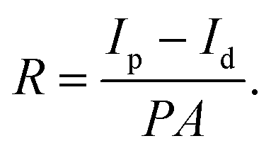
The sensitivity of a photodetector (PD) is commonly reported as responsivity, which is given by the ratio of the change in current under illumination to the incident optical power:
 | (1) |
where R is the responsivity (A W−1), Ip is the current under illumination, Id is the dark current, P is the optical power density (3.59 mW cm−2), and A is the effective area under irradiation (∼1 × 10⁻³ cm2). The calculated responsivity was ∼0.01 A W−1. Note that all the devices were fabricated and tested in an ambient environment, therefore device performance may be underestimated due to exposure to oxygen and moisture in air. The response time of the IR PD was measured and is shown in Fig. 4e and f. It shows a consistent fast response upon numerous cycles of on–off testing. The calculated rise time and decay time were 4.6 ms and 4.7 ms, respectively.
Conclusion
In this work, we have demonstrated that EPD can be utilized for conformal coating of in-solution ligand exchanged QDs onto flat, patterned, and textured substrates. Controlling QD surface charging through solvent engineering allows the QDs to remain stable during the deposition process, while still being effectively “driven” to the desired electrode by an applied field. The QDs deposit onto conductive or moderately conductive substrates, allowing for the possibility of selective deposition through masking and/or electrode design. The speed and efficiency of EPD make it a promising technique for single-step conformal deposition of QD films in a high throughput environment, such as those used in industry. Additionally, the selectivity of EPD, only depositing onto substrates with an applied bias, enables challenging/new device architecture design of a variety of QD electronic devices, such as QLEDs and Q-photodetectors. As EPD becomes more prevalent in QD film fabrication, future work should focus on addressing potential limitations, such as the creation of extremely thick films (>10 microns), which may be hindered by weakening electric fields, and the minimum area/separation achievable when creating QD arrays.Methods
Chemicals
All chemicals were purchased from Sigma Aldrich and used without further purification. Oleylamine [70% technical grade] (OLA), PbBr2 [>98%], 2,6-diflouropyridine [99%] (DFP), N-dimethylformamide (DMF), hexane, acetonitrile (ACN), ammonium iodide (NH4I), chloroform (CHCl3), di-i-butylphosphine (DIP), tri-n-octylphosphine (TOP), and selenium shot (Se) were used. 2 M TOPSe was made in a glovebox by magnetically stirring 10 mmol Se shot in 5 mL of TOP until fully dissolved.Synthesis of PbSe QDs
Synthesis of the PbSe QDs closely follows the work of Lin et al.25 In a typical reaction, a three-neck flask was filled with 8 mmol of PbBr2, 8 mL of OLA, and 16 mL of ODE and heated under vacuum at 110 °C for 120 min to obtain a clear solution. The flask was then filled with N2 and the temperature was raised to 120 °C. A mixture comprising 0.1 mL of DIP, 2 mL of OLA, and 1 mL of 2 M TOPSe was injected into the lead precursor solution. The flask was removed from heat immediately after the injection and allowed to cool to room temperature; PbSe QDs with 4.0 nm diameter were obtained. PbSe QDs with other sizes can be synthesized by altering the reaction time and/or temperature. After the reaction, the QDs were cleaned in air by the addition of CHCl3 and ACN followed by centrifugation. After centrifugation, the supernatant was discarded and the QDs were cleaned 3 more times via the addition of CHCl3, for redispersion, followed by ACN addition, for destabilization, and subsequent centrifugation. After the final cleaning step, the QDs were redispersed in hexane with a concentration of ∼10 mg mL−1.In-solution ligand exchange
In-solution ligand exchange followed a procedure reported by Lin et al.25 In a typical ligand exchange, 500 mg of NH4I was dissolved in 5 mL of DMF in a centrifuge tube after which 5 mL of PbSe QDs (10 mg mL−1) in hexane was layered on top of the DMF–NH4I solution. After shaking for 10 seconds, the PbSe QDs readily transferred into the DMF phase. Once all QDs had transferred, the top layer of hexane was removed via a syringe. CHCl3 was added to the DMF–QD solution to destabilize the suspension followed by centrifugation to bring the QDs out of solution, at which point the supernatant was discarded. After ligand exchange, the QDs were readily dispersed in DFP with a concentration of 10–15 mg mL−1 without further cleaning.Absorption and FTIR measurements
Absorption measurements of the PbSe QD solution were performed with a PerkinElmer Lambda 950 spectrometer using a 1 mm path length cuvette. FTIR measurements, to confirm ligand exchange, were performed on the PbSe QD films drop-cast onto ZnSe windows and measured using a Bruker Vertex 70 FTIR spectrometer.Electric field-driven assembly of ligand-exchanged QDs
After ligand exchange, the PbSe QDs capped with NH4I and dispersed in DFP were controllably deposited onto conductive or moderately conductive substrates using an applied electric field. Substrates were flat, patterned or textured with deposition only on regions with an electric field; examples of selective deposition are shown in Fig. S6.† Notably, the PbSe–NH4I QDs in DFP did not respond to the electrical field without the addition of a nonpolar antisolvent. Solvent engineering was needed to destabilize the PbSe–NH4I QD colloidal solution for efficient field-driven assembly. By titrating hexane into the native PbSe–NH4I QDs/DFP solution up to a DFP:hexane volume ratio of 1:0.8, the nanocrystals began to respond to the electric field and were deposited exclusively on the positive electrode. Increasing the hexane titration ratio typically resulted in a higher deposition rate within the DFP:hexane ratio range of 1:0.8 to 1:2. However, the PbSe–NH4I QDs demonstrated decreased colloidal stability when the volume of hexane exceeded DFP by a factor of 2, leading to the formation of a porous film rather than a homogeneous film and eventual sedimentation of the solution. Typical electric fields and deposition times in this work used were 0.2 V mm−1 and 2–10 minutes. The thickness of the dry QD films was measured using a Dektak stylus profilometer (Bruker, Dektak XT). See Table S1† for the film thickness of the PbSe QD films prepared under a variety of EPD conditions.
Measurement and calculation of the conductivity of the suspension
The conductivity of the PbSe quantum dots (QDs) capped with NH4I in DFP was measured using a Keithley 2400 source meter and a parallel plate electrode geometry. Hexane was titrated into the suspension while monitoring the change in conductivity. The corresponding conductivity was calculated via the following equation: | (2) |
| σ = nqμ, | (3) |
X-Ray scattering measurements and analysis
GISAXS was performed at the Advanced Light Source (ALS) beamline 7.3.3 using 10 keV radiation. Scattering photons were collected using a Pilatus 2M detector. The data were processed with Igor Pro-based software packages written by, and available for download from, Ilavsky and Jemian.45Fabrication of PbSe-based infrared detectors
To generate devices, a homogeneous PbSe–NH4I film with a thickness of ∼200 nm was assembled on a non-insulating substrate, such as intrinsic Si (MSE PRO Intrinsic Prime Grade Silicon Wafer 〈100〉, SSP, >20000 ohm-cm), via EPD. A typical deposition process involved applying an electric field of 0.4 V mm−1 to the PbSe–NH4I QDs dissolved in a 1:1 (volume ratio) mixture of DFP:hexane for 5 minutes. After deposition, the film was removed from the solvent mixture and allowed to dry in air. Subsequently, a parallel silver electrode with a spacing of ∼100 μm was deposited onto the PbSe–NH4I film using a shadow mask. Note that all the QD devices fabricated in this work were manufactured and tested in an ambient environment.
Textured silicon substrates
To create a series of pyramidal structures covering the surface area of a wafer, we followed the etching procedure developed by Leon et al.41 The etching solution consisted of 12.8 g of KOH pellets (2.3 wt%) dissolved in 500 mL of deionized water and 55.6 mL of isopropanol alcohol (10 vol%) was heated up to 72 °C. The intrinsic Si wafers were etched in the solution for 3 hours with manual agitation every 10–15 minutes to prevent bubble buildup on the surface of the wafer that can lead to surface defects. This method results in complete coverage of the silicon surface with pyramidal structures having a base of 12 ± 2 μm. An SEM image of the as-prepared textured Si is shown in Fig. S7.†QCM study of the field-driven assembly of QDs
A quartz crystal microbalance (QCM) [Stanford Research System 200] was employed to study the rate of QD deposition. A home-built closed QCM cell requiring a solution volume of ∼5 ml was used; photos of the QCM cell can be seen in Fig. S8.† Frequency change and current change were monitored in situ throughout the deposition process.46 The frequency change was converted to the mass of the QDs deposited using| Δf = −Cf·Δm | (4) |
Photoresponse measurements
Photoresponse measurements were performed using a compact broadband light source, Thorlabs SLS203L, with a 1200 nm optical filter. The resulting light power at 1200 nm was found to be 28.1 μW using a Thorlabs S148C detector on a PM100D power meter. We performed light and dark voltage sweeps as well as on/off measurements under an applied bias of 2 V.Author contributions
T. N., X. X. and C. O. conceived the project and performed the experimental studies and analysis. B. F. helped in designing the QCM experiment and analysis. J. Z. etched silicon wafers and performed EDS mapping. T. N. and X. X. wrote the first draft of the manuscript, which was edited by all authors.Data availability
The authors confirm that the data supporting the findings of this study are available within the article and its ESI,† and the raw data are available from the corresponding authors upon reasonable request.Conflicts of interest
There are no conflicts of interest to declare.Acknowledgements
This work was performed under the auspices of the U.S. Department of Energy by Lawrence Livermore National Laboratory under Contract DE-AC52-07NA27344 and supported by LDRD 22-LW-054. LLNL IM release number LLNL-TM-865780. X-ray scattering experiments were performed on beamline 7.3.3 at the Advanced Light Source supported by the Office of Science, Office of Basic Energy Sciences, the U.S. Department of Energy under contract no. DE-AC02-05CH11231.References
- Q. Dai, Y. Wang, X. Li, Y. Zhang, D. J. Pellegrino, M. Zhao, B. Zou, J. Seo, Y. Wang and W. W. Yu, ACS Nano, 2009, 3, 1518–1524 CrossRef PubMed.
- A. P. Alivisatos, Science, 1996, 271, 933–937 CrossRef.
- G. Konstantatos, I. Howard, A. Fischer, S. Hoogland, J. Clifford, E. Klem, L. Levina and E. H. Sargent, Nature, 2006, 442, 180–183 CrossRef PubMed.
- R. Guo, M. Zhang, J. Ding, A. Liu, F. Huang and M. Sheng, J. Mater. Chem. C, 2022, 10, 7404–7422 RSC.
- N. Ahn, C. Livache, V. Pinchetti and V. I. Klimov, Chem. Rev., 2023, 123, 8251–8296 CrossRef PubMed.
- V. Wood and V. Bulović, Nano Rev., 2010, 1, 5202 CrossRef PubMed.
- E. Jang and H. Jang, Chem. Rev., 2023, 123, 4663–4692 CrossRef PubMed.
- G. Almeida, R. F. Ubbink, M. Stam, I. du Fossé and A. J. Houtepen, Nat. Rev. Mater., 2023, 8, 742–758 CrossRef CAS.
- M. Park, D. Choi, Y. Choi, H. Shin and K. S. Jeong, ACS Photonics, 2018, 5, 1907–1911 CrossRef CAS.
- P. Guyot-Sionnest, M. M. Ackerman and X. Tang, J. Chem. Phys., 2019, 151, 060901 CrossRef.
- T. Nakotte, S. G. Munyan, J. W. Murphy, S. A. Hawks, S. Kang, J. Han and A. M. Hiszpanski, J. Mater. Chem. C, 2022, 10, 790–804 RSC.
- Y. Liu, J. Tolentino, M. Gibbs, R. Ihly, C. L. Perkins, Y. Liu, N. Crawford, J. C. Hemminger and M. Law, Nano Lett., 2013, 13, 1578–1587 CrossRef CAS PubMed.
- R. D. Schaller and V. I. Klimov, Phys. Rev. Lett., 2004, 92, 186601 CrossRef CAS PubMed.
- D. V. Talapin and C. B. Murray, Science, 2005, 310, 86–89 CrossRef CAS PubMed.
- F. P. García De Arquer, D. V. Talapin, V. I. Klimov, Y. Arakawa, M. Bayer and E. H. Sargent, Science, 2021, 373, eaaz8541 CrossRef PubMed.
- M. Ruggieri, E. Colantoni, E. Marconi, A. Fabbri, P. Branchini, L. Colace, L. Tortora and A. De Iacovo, ACS Appl. Electron. Mater., 2023, 5, 5642–5650 CrossRef CAS.
- T. D. McCrea, A. O. Darus, H. B. Anderson, H. Mei, C. Pan, M. D. Hammig, C.-H. Chang, G. S. Herman and H. Yang, Nucl. Instrum. Methods Phys. Res., Sect. A, 2023, 1048, 167979 CrossRef CAS.
- J. Z. Fan, M. Vafaie, K. Bertens, M. Sytnyk, J. M. Pina, L. K. Sagar, O. Ouellette, A. H. Proppe, A. S. Rasouli, Y. Gao, S.-W. Baek, B. Chen, F. Laquai, S. Hoogland, F. P. G. D. Arquer, W. Heiss and E. H. Sargent, Nano Lett., 2020, 20, 5284–5291 CrossRef CAS PubMed.
- J.-H. Choi, A. T. Fafarman, S. J. Oh, D.-K. Ko, D. K. Kim, B. T. Diroll, S. Muramoto, J. G. Gillen, C. B. Murray and C. R. Kagan, Nano Lett., 2012, 12, 2631–2638 CrossRef CAS PubMed.
- C. R. Kagan and C. B. Murray, Nat. Nanotechnol., 2015, 10, 1013–1026 CrossRef CAS PubMed.
- M. C. Weidman, K. G. Yager and W. A. Tisdale, Chem. Mater., 2015, 27, 474–482 CrossRef CAS.
- G. H. Carey, K. W. Chou, B. Yan, A. R. Kirmani, A. Amassian and E. H. Sargent, MRS Commun., 2013, 3, 83–90 CrossRef CAS.
- A. Shrestha, M. Batmunkh, A. Tricoli, S. Z. Qiao and S. Dai, Angew. Chem., Int. Ed., 2019, 58, 5202–5224 CrossRef CAS PubMed.
- F. Dubois, B. Mahler, B. Dubertret, E. Doris and C. Mioskowski, J. Am. Chem. Soc., 2007, 129, 482–483 CrossRef CAS PubMed.
- Q. Lin, H. J. Yun, W. Liu, H.-J. Song, N. S. Makarov, O. Isaienko, T. Nakotte, G. Chen, H. Luo, V. I. Klimov and J. M. Pietryga, J. Am. Chem. Soc., 2017, 139, 6644–6653 CrossRef CAS PubMed.
- X. Lan, M. Chen, M. H. Hudson, V. Kamysbayev, Y. Wang, P. Guyot-Sionnest and D. V. Talapin, Nat. Mater., 2020, 19, 323–329 CrossRef CAS PubMed.
- T. Qin, G. Mu, P. Zhao, Y. Tan, Y. Liu, S. Zhang, Y. Luo, Q. Hao, M. Chen and X. Tang, Sci. Adv., 2023, 9, eadg7827 CrossRef CAS PubMed.
- V. Pejovic, E. Georgitzikis, J. Lee, I. Lieberman, D. Cheyns, P. Heremans and P. E. Malinowski, IEEE Trans. Electron Devices, 2022, 69, 2840–2850 CAS.
- A. Sharma, J. Kedia and N. Gupta, Opt. Eng., 2021, 60, 090901 Search PubMed.
- A. K. Sood, J. W. Zeller, A. W. Sood, R. E. Welser, P. Ghuman, S. R. Babu, S. D. Gunapala, L. S. Chaudhary and H. Efstathiadis, in Infrared Sensors, Devices, and Applications XI, ed. A. K. Sood, P. Wijewarnasuriya and A. I. D'Souza, SPIE, San Diego, United States, 2021, p. 13 Search PubMed.
- L. Besra and M. Liu, Prog. Mater. Sci., 2007, 52, 1–61 CrossRef.
- X. Xu, K. E. Kweon, S. Keuleyan, A. Sawvel, E. J. Cho and C. Orme, Small, 2021, 17, 2101166 CrossRef PubMed.
- M. A. Islam and I. P. Herman, Appl. Phys. Lett., 2002, 80, 3823–3825 CrossRef.
- M. A. Islam, Y. Xia, B. J. Kraines and I. P. Herman, MRS Online Proc. Libr., 2002, 737, 55 CrossRef.
- A. Hassinen, I. Moreels, K. De Nolf, P. F. Smet, J. C. Martins and Z. Hens, J. Am. Chem. Soc., 2012, 134, 20705–20712 CrossRef PubMed.
- J.-L. M. Abboud and R. Notari, Pure Appl. Chem., 1999, 71, 645–718 CrossRef.
- Y. Yu, D. Yu and C. A. Orme, Nano Lett., 2017, 17, 3862–3869 CrossRef PubMed.
- R. A. Miranda-Quintana and J. Smiatek, J. Mol. Liq., 2021, 322, 114506 CrossRef.
- D. N. Dirin, S. Dreyfuss, M. I. Bodnarchuk, G. Nedelcu, P. Papagiorgis, G. Itskos and M. V. Kovalenko, J. Am. Chem. Soc., 2014, 136, 6550–6553 CrossRef PubMed.
- I. Moreels, K. Lambert, D. De Muynck, F. Vanhaecke, D. Poelman, J. C. Martins, G. Allan and Z. Hens, Chem. Mater., 2007, 19, 6101–6106 CrossRef.
- J. J. D. Leon, A. M. Hiszpanski, T. C. Bond and J. D. Kuntz, Adv. Opt. Mater., 2017, 5, 1700080 CrossRef.
- H. Kumar Raut, V. Anand Ganesh, A. Sreekumaran Nair and S. Ramakrishna, Energy Environ. Sci., 2011, 4, 3779–3804 RSC.
- C. L. Tan and H. Mohseni, Nanophotonics, 2018, 7, 169–197 CrossRef.
- D. S. Hobbs, Proc. SPIE Volume 5786, Window and Dome Technologies and Materials IX, 2005, 5786, p. 349, DOI:10.1117/12.604537.
- J. Ilavsky and P. R. Jemian, J. Appl. Crystallogr., 2009, 42, 347–353 CrossRef.
- K. R. Panta, C. A. Orme and B. N. Flanders, J. Colloid Interface Sci., 2023, 636, 363–377 CrossRef PubMed.
Footnotes |
| † Electronic supplementary information (ESI) available. See DOI: https://doi.org/10.1039/d4nr04620j |
| ‡ These authors contributed equally to this work. |
| This journal is © The Royal Society of Chemistry 2025 |