
 Open Access Article
 This Open Access Article is licensed under a
 Creative Commons Attribution 3.0 Unported Licence
Advancing transistor-based point-of-care (POC) biosensors: additive manufacturing technologies and device integration strategies for real-life sensing
Xiaoao
Shi
ab,
Haihui
Pu
ab,
Lewis L.
Shi
c,
Tong-Chuan
He
c and
Junhong
Chen
 *ab
*ab
aChemical Sciences and Engineering Division, Physical Sciences and Engineering Directorate, Argonne National Laboratory, Lemont, Illinois 60439, USA. E-mail: junhongchen@uchicago.edu
bPritzker School of Molecular Engineering, University of Chicago, Chicago, Illinois 60637, USA
cMolecular Oncology Laboratory, Department of Orthopaedic Surgery and Rehabilitation, Chicago, Illinois 60637, USA
First published on 18th March 2025
Abstract
Infectious pathogens pose a significant threat to public health and healthcare systems, making the development of a point-of-care (POC) detection platform for their early identification a key focus in recent decades. Among the numerous biosensors developed over the years, transistor-based biosensors, particularly those incorporating nanomaterials, have emerged as promising candidates for POC detection, given their unique electronic characteristics, compact size, broad dynamic range, and real-time biological detection capabilities with limits of detection (LODs) down to zeptomolar levels. However, the translation of laboratory-based biosensors into practical applications faces two primary challenges: the cost-effective and scalable fabrication of high-quality transistor sensors and functional device integration. This review is structured into two main parts. The first part examines recent advancements in additive manufacturing technologies—namely in screen printing, inkjet printing, aerosol jet printing, and digital light processing—and evaluates their applications in the mass production of transistor-based biosensors. While additive manufacturing offers significant advantages, such as high quality, cost-effectiveness, rapid prototyping, less instrument reliance, less material waste, and adaptability to diverse surfaces, challenges related to uniformity and yield remain to be addressed before these technologies can be widely adopted for large-scale production. The second part focuses on various functional integration strategies to enhance the practical applicability of these biosensors, which is essential for their successful translation from laboratory research to commercialization. Specifically, it provides a comprehensive review of current miniaturized lab-on-a-chip systems, microfluidic manipulation, simultaneous sampling and detection, wearable implementation, and integration with the Internet of Things (IoT).
 Xiaoao Shi | Xiaoao Shi is currently pursuing a Ph.D. under the supervision of Dr Junhong Chen at the Pritzker School of Molecular Engineering, University of Chicago. He received his bachelor's degree in biotechnology from the University of California, San Diego. His research interests lie in the development of novel two-dimensional nanomaterial-based field-effect transistor biosensors for biomedical applications, including the detection of bacterial infections and aerosol pathogen monitoring. |
 Haihui Pu | Haihui Pu received his Ph.D. from the University of Wisconsin Milwaukee (UWM) in 2015. Before joining the University of Chicago as a Staff Scientist, he completed a Postdoctoral Appointment at UWM and worked as a Sensor Scientist for NanoAffix Science, LLC. Pu received his M.S. degree from Fudan University and his B.S. degree from Nanjing University of Science and Technology in China. His research focuses on first-principles/molecular dynamics simulations and statistical thermodynamics modeling on novel two-dimensional nanomaterials for environmental and energy applications, which include field-effect transistor nanosensors for detecting various target analytes of interest and energy storage devices. |
 Lewis L. Shi | Lewis Shi, MD, is an orthopaedic surgeon who specializes in shoulder injuries and sports medicine. His expertise includes rotator cuff and labral tears, shoulder dislocation, and total and reverse shoulder replacement. As an active researcher, Dr Shi has published more than 100 peer-reviewed scientific articles and 10 book chapters. His current research focuses on the molecular basis of rotator cuff tear and biomechanics of shoulder arthritis. Dr Shi frequently lectures nationally and internationally, and he teaches courses sponsored by national orthopaedic associations. Dr Shi is also the editor-in-chief of the Journal of Shoulder and Elbow Arthroplasty. |
 Tong-Chuan He | Tong-Chuan He, MD, PhD is a tenured Associate Professor and the Director of the Molecular Oncology Laboratory in the Department of Orthopedic Surgery and Rehabilitation Medicine at the University of Chicago Medical Center. The He lab consists of a dynamic group of basic science investigators and physician scientists, who have diverse expertise and a broad range of interests in basic and translational research in stem cell biology, cancer biology and regenerative medicine. He has co-authored over 400 peer-reviewed publications with more than 51 |
 Junhong Chen | Junhong Chen is currently a Crown Family Professor of Molecular Engineering at Pritzker School of Molecular Engineering at the University of Chicago and lead water strategist at Argonne National Laboratory. Chen received his Ph.D. in mechanical engineering from the University of Minnesota in 2002. His research interest lies in molecular engineering of nanomaterials and nanodevices, particularly hybrid nanomaterials featuring rich interfaces and nanodevices for sustainable energy and the environment. His approach is to combine multidisciplinary experiments with first-principles calculations to design and discover novel nanomaterials for engineering various sensing and energy devices with superior performance. |
1. Introduction
The long-lasting pandemic of COVID-19 has reiterated that infectious diseases remain one of the leading causes of death worldwide.1,2 According to the latest report from the World Health Organization (WHO), there have been over 775 million COVID-19 cases cumulatively and SARS-CoV-2 has caused more than 7 million deaths globally.3 Furthermore, the emergence of new pathogens along with the resurgence of known pathogens such as SARS-CoV-2, tuberculosis, anthrax, and influenza poses enormous challenges to public health and the economy worldwide. These highly infectious pathogens can be transmitted through air, water, food, and feces, and can enter the human body through the eyes, mouths, nostrils, ears, urogenital openings, or wounds that breach the skin barriers.4 Rapid and accurate detection of infectious pathogens is critical for preventing outbreaks of new epidemics and improving public health.5,6 In 2016, the WHO announced ASSURED criteria for point-of-care (POC) detections: Affordable, Sensitive, Specific, User-friendly, Rapid and Robust, Equipment-free and Deliverable. In May 2023, the WHO began launching global networks for pathogen detection.7,8Compared with traditional biosensing techniques (e.g., polymerase chain reaction (PCR), colony-based culture and immuno-based assays) that rely heavily on trained professionals and sophisticated laboratory instruments, miniaturized biosensors have garnered significant interest over the past few decades, owing to their suitability for POC diagnostics as well as their potential in healthcare monitoring, environmental surveillance, and food safety industries.9–13 POC biosensors are devices that recognize a specific type of biomolecule (DNA, antibody, antigen, bacteria, protein, virus) and generate measurable signals for real-time diagnosis through electrical, optical, biological or mechanical mechanisms. Among the most widely used POC biosensors are electronic- and optical-based systems, such as glucometers and colorimetric lateral flow assays (LFAs).14,15 Depending on the signal type, the optical biosensors can be further classified into fluorescence-based biosensors, surface-enhanced Raman scattering-based biosensors, surface plasmon resonance (SPR)-based biosensors and photonic crystal-based biosensors.16–21 However, when detecting low-concentration analytes, the signal produced by many optical biosensors falls within a range difficult to distinguish with the naked eye, requiring bulky and complex equipment to translate the optical signal into readable results. This requirement significantly hinders the transition of optical biosensors from laboratory settings to portable commercial POC devices.
In contrast, electronic-based biosensors, which directly convert the presence and concentration of analytes into electrical signals, offer a highly promising alternative for POC due to their miniaturized form and ease of integration.21–23 These biosensors can be classified into four main categories based on their detection mechanisms: amperometry, potentiometry, impedance, and transistor-based sensing platforms. Among them, transistor-based biosensors, such as field-effect transistor (FET) biosensors and organic electrochemical transistor (OECT) biosensors, stand out as superior candidates due to their unique electronic characteristics, compact size, broad dynamic range, and real-time biological detection with LODs down to zeptomolar levels and, in some cases, even enabling the evaluation of single molecules or particles.24,25 A transistor-based biosensor is defined as a three-terminal system comprising source, drain, and gate electrodes, along with a semiconducting material channel and a highly sensitive and selective biorecognition layer (Fig. 1a & b). As target analytes bind to probes on the sensing surface, the induced electric field change results in a current/impedance change between the source and drain electrodes.26 This calibrated current/impedance change can be used to determine the presence and the concentration of the analytes.
 | ||
| Fig. 1 (a) Schematic of FET bioelectronics.27 (b) Selective binding in recognition events: specific capturing antibody binding antigen biomarker; DNA probe binding complementary DNA genetic biomarker; enzyme (glucose oxidase) electrochemical reaction with substrate (glucose).27 “Reproduced from ref. 27 with permission from Wiley, copyright 2019”. (c) Schematic illustration of the changes occurring in the electrolyte/polymer interface for OECTs working in depletion (top) and accumulation mode (middle for p-type and bottom for n-type).28 “Reproduced from ref. 28 with permission from Wiley, copyright 2021”. (d). Schematic of FET biosensor structure with all key components.29 “Reproduced from ref. 29 with permission from Springer Nature, Creative Commons Attribution (CC BY) license, copyright 2017”. (e). Schematic of an InSe-based FET fabrication in traditional lithography.30 “Reproduced from ref. 30 with permission from Springer Nature, Creative Commons Attribution (CC BY) license, copyright 2019”. | ||
Traditional FET sensors operate in two characteristic states: the “on” state and the “off” state. In the off state, carriers in the channel are depleted, causing no current flow between source and drain electrodes, while in the on state the carriers in the channel are enhanced, allowing current flow between the source and drain electrodes. The on/off current ratio, as the name suggests, is the ratio between the on-state current and off-state current and is one of the important critical performance metrics for assessing the switching ability of sensors.26 A high switching ability typically indicates better sensitivity of the FET-based biosensors and can be calculated through the transfer curve plot (source drain current Idsvs. gate source voltage Vgs). Switching ability (on/off ratio) is controlled by the channel material selection, insulator quality, and channel design etc. In ideal situations, assuming (1) there is no leakage through the insulator layer, (2) the contacts are ideal, and (3) there is no scattering of electrons by impurities in the semiconductor channel, the Ids can be formulated as eqn (1).
 | (1) |
 | (2) |
Organic electrochemical transistors (OECTs) are relatively new and promising transistor-type candidates for next-generation biosensing, given their unique mechanism of operation, which involves the modulation of electrolyte concentration to regulate the channel conductivity (Fig. 1c).24,32 OECTs are three terminal devices similar to FET, but with semiconductor channel materials replaced by soft ion-permeable conducting polymers such as poly(3,4-ethylenedioxythiophene) polystyrene sulfonate (PEDOT:PSS). Unlike FETs, OECTs operate in an electrolyte solution, as the channel and the gate electrode must be bridged by electrolyte for proper functioning. The gate voltage controls the electrochemical doping/dedoping of the conductive polymer channel, leading to variations in source–drain current. The usage of soft conducting polymers enables OECTs to maintain electrical performance under bending cycles, making them promising candidates for wearable device applications. OECT devices have demonstrated efficacy in the detection of ions, various biomolecules, antibody–antigen binding events, and stress and strains.33–37
In transistor-based biosensors, the selection of conducting channel materials substantially governs the overall performance of the transistor sensor. Nanomaterials have been extensively utilized as semiconductor channels in the FET fabrication due to their large surface-to-volume ratio, favorable semiconducting properties, flexibility, and stretchability. A schematic of a typical FET biosensor structure with all the key components is illustrated in Fig. 1d. Currently, multi-step-based lithography remains the gold standard for the laboratory-scale fabrication of transistor-based biosensors. For instance, lithography followed by metal deposition is employed for the fabrication of electrodes in various FET-based biosensors,38–40 while soft lithography is used for fabrication of the electrolyte gates for various OECT-based biosensors.12,37,41,42 Chemical vapor deposition (CVD) and spin coating are commonly used to deposit various nanomaterials—graphene, MoS2, nanotubes, and organic materials—as a transducing channel.43–48 Although the traditional CVD processes provide high-quality nanomaterial layers, their application in the mass-scale fabrication of 2D nanomaterials is limited by high costs, low yields, tedious material transfer processes and usage of a high-temperature furnace.49 The spin coating method is noted for its good control over the thickness and uniform film quality on a small-area substrate, achieving high reproducibility through adjustments in speed, time and acceleration.50 However, this reproducibility tends to decrease as the substrate size increases. A schematic of an InSe FET-based biosensor, fabricated using CVD and traditional lithography, is illustrated in Fig. 1e. In contrast to these traditional methods of fabricating biosensor devices, additive manufacturing (AM) showed tremendous advantages, including ease of prototyping, reduced expensive material usage, reduced fabrication time and less instrument reliance. The capabilities of AM are continuously extended by the scientific community into a wide variety of applications, including medical diagnostics, food security, energy storage, electronic skin, artificial organs, and in-body scaffolds.51–55
Since most nanomaterials exhibit excellent compatibility with AM technology, numerous studies have been carried out on the integration of nanomaterials with AM for transistor biosensor fabrication, capitalizing on both the advantage of the material properties and the cost-effective fabrication techniques.56–61 This review will examine the fabrication of nanomaterial-based transistor-based biosensors using various AM techniques, analyzing their advantages and challenges. However, successful mass fabrication alone is insufficient for translating laboratory biosensors into commercial devices. Functional device integration is the next critical step in this transition. In the second main part, this review provides a comprehensive examination on various functional device integration strategies for transistor-based biosensors, with a focus on enhancing their practical applicability.
2. Additive manufacturing for transistor device fabrication
AM (or 3D printing) is defined as the process of creating physical objects through the layer-by-layer deposition of materials directly from digital design files.62 While printing technologies have been widely adopted in a variety of fields, such as T-shirt printing a long time ago, it was not until 1986, with the publication of Chuck Hull's patent, that the potential of AM (3D printing) started to be recognized in sensor development.63 3D printing technologies integrate the device design with device fabrication in one step, achieving high resolutions and significantly cutting down the time and effort required for device optimization.64,65 Although the first-generation 3D printers were prohibitively expensive for research usage, since the last decade, commercial desktop 3D printers have become available at prices ranging from $1000–$4000.66 In the near future, 3D printing may evolve into a mass production method, facilitating the transition of biosensors from off-site laboratories to on-site, customizable detections. Several promising techniques, such as screen printing, inkjet printing, aerosol jet printing and digital light processing, have already been used in the fabrication of transistor-based biosensors.Screen printing
Screen printing has been utilized in the fabrication of electrodes from the early 1990s. Compared with pad printing and roll-to-roll printing, screen printing has the capability of bridging the gap between laboratory prototypes and commercialized devices.67 The screen printing process can be divided into three stages: in the first stage, the ink floods into the mesh and occupies the open area (Fig. 2a); in the second stage, the ink flows into contact with the substrate due to gravity (Fig. 2b); and in the final stage, the mesh is lifted off vertically and the ink forms filaments by overcoming the cohesive forces (Fig. 2c). This final stage can be further divided into 4 substages identified by Messerschmitt: adhesion of ink to the substrate, extension of the mesh, flow of the ink into filaments, and separation of the ink filaments.68 The filament structure that results from this transfer process is closely related to the ink viscosity, cohesive and adhesive forces, pseudoplasticity, and mesh angles.69 The resolution of screen printing in producing ultrathin (<70 μm) filaments is still an area of active research.53,70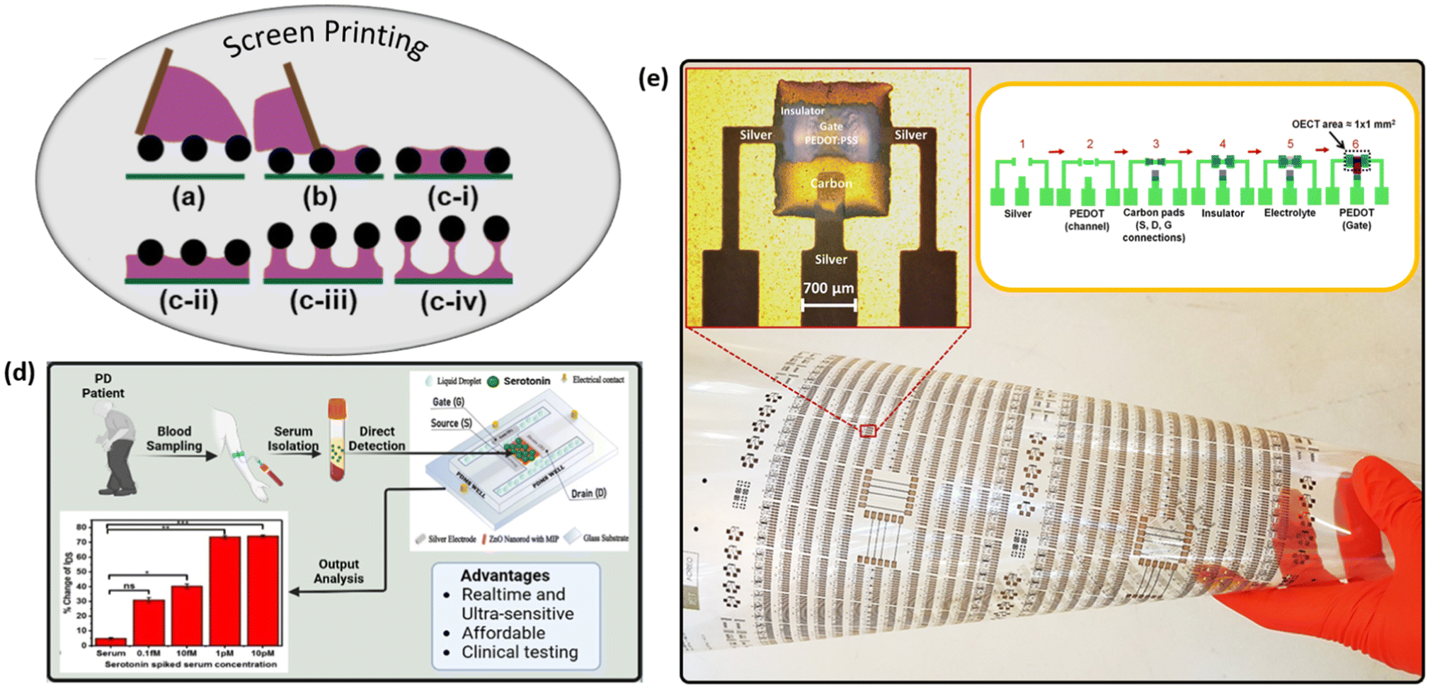 | ||
| Fig. 2 Schematic of screen printing mechanism69 (a) Excess fluid on the mesh after a flood stroke. (b) Squeezing forces the screen into contact with the substrate and fills the cavities with ink. (c) (i–iv) The screen separates from the substrate, and ink is pulled from mesh. “Reproduced from ref. 69 with permission from the American Chemical Society, CC-BY-NC-ND 4.0, copyright 2021”. (d). Screen-printed ZnO nanorod FET for serotonin detection in clinical samples with a molecularly imprinted polymer interface.71 “Reproduced from ref. 71 with permission from the American Chemical Society, copyright 2023”. (e). Sequence of six printed layers and the approximate footprint per OECT.72 “Reproduced from ref. 72 with permission from Springer Nature, Creative Commons Attribution (CC BY) license, copyright 2020”. | ||
Screen-printing enables the easy reproduction of designs on a variety of substrate surfaces, such as ductile polymers, paper, ceramics, and glass. It offers enormous versatility in electrode design and material selection while maintaining mass-producibility, cost-effectiveness, and reproducibility.72–74 Over the past decades, screen printing has been extensively utilized in the fabrication of electrodes, which are used in various biosensors for pathogen and biomolecular detection.75–77 However, using screen printing to fabricate the transducing channel in transistor-based biosensors still presents significant challenges due to limitations in printing resolution and potential damage from contact printing. As a result, the application of screen printing in FET-based biosensor fabrication remains limited, as it is not well-suited for one-step fabrication of sensors.
Only a few studies have attempted to leverage the cost-effectiveness and rapid prototyping capabilities of screen-printed electrodes for FET-based biosensor development. Sinha et al. fabricated molecularly imprinted polymer (MIP)-modified ZnO nanorod FET for serotonin detection, achieving a detection range from 0.1 fM to 10 pM in approximately 45 seconds (Fig. 2d).71 In this process, an optimized 1![[thin space (1/6-em)]](https://www.rsc.org/images/entities/char_2009.gif) :4 diluted silver ink was used to screen-print source, drain, and gate electrodes of appropriate thickness. Subsequently, an Al- and Mg-doped ZnO thin film was deposited using the sol–gel method in a standard clean bench, followed by chemical bath deposition to grow ZnO nanorods. Careful control over the thickness of the screen-printed metal electrode layer is crucial, as it directly affects sensor performance. Excessive electrode thickness can lead to nonconformal growth of the ZnO channel layer, ultimately reducing the sensor's On/Off current ratio.
:4 diluted silver ink was used to screen-print source, drain, and gate electrodes of appropriate thickness. Subsequently, an Al- and Mg-doped ZnO thin film was deposited using the sol–gel method in a standard clean bench, followed by chemical bath deposition to grow ZnO nanorods. Careful control over the thickness of the screen-printed metal electrode layer is crucial, as it directly affects sensor performance. Excessive electrode thickness can lead to nonconformal growth of the ZnO channel layer, ultimately reducing the sensor's On/Off current ratio.
Conversely, screen printing has been widely adopted for the fabrication of electrolyte gates in organic electrochemical transistors (OECTs). Zabihipour et al. explored the use of screen printing in OECT fabrication and achieved an overall yield of 99.7%, thus demonstrating the potential of this technique for large-scale production.72 The fabrication process of a six-layered OECT using screen printing is shown in Fig. 2e, namely the electrode, channel, connections, insulator, electrolyte and gate. In their study, up to 760 OECTs of 1 mm2 area were fabricated in a single batch on a PET sheet and only two devices exhibit a On/Off ratio less than 400. However, as OECT designs shrink to channel sizes as small as 150 μm × 100 μm, device performance can exceed an On/Off ratio of 100000, but the yield decreases to below 98%, and uniformity across the entire sheet becomes worse. While such a manufacturing yield may be sufficient for standalone transistors, further improvements are necessary for printed circuitry applications. Contat-Rodrigo et al. also demonstrated the potential of screen printing for OECT fabrication by printing PEDOT:PSS onto a polyester film to create a flexible OECT sensor for ascorbic acid (AA) detection. The biosensor achieved a detection range from 10−8 M to 10−2 M, highlighting the feasibility of screen-printed OECT for detecting food-based AA with a concentration typically in the millimolar (mM) range.78
Despite its promise, several challenges remain in the application of screen-printing for transistor-based biosensor fabrication. When fabricating multilayer structures at ambient temperature, yield and reliability during mass-production via screen-printing are major concerns.72 System clogging, induced by an agglomeration of particles due to the evaporation of surfactants and solvents in the printing paste, is another common technical issue encountered during large-scale production, leading to high material waste.79 Several solutions have been proposed to address the system clog issue, including the dilution of particle-based ink and the use of aqueous combustible molecular precursor-based clog-free ink.80,81 However, optimizing screen-printing inks remains experimentally tedious, as it is closely tied to factors such as viscosity, adhesive and cohesive forces in the ink, which limits the broader application of screen-printing.
Inkjet printing
Inkjet printing (IJP) is a non-impact printing technique that deposits nanomaterials in the form of a colloidal dispersion, droplet by droplet, through micro-meter scale nozzles. It is recognized as a material-saving deposition technique for printing functional patterns.82 A typical inkjet-printer consists of three main components: a motion stage, control systems (including the printing heads), and a vision system.83 The motion stage enables movement along the X–Y axis to print patterns, while the control system facilitates Z-axis movement of the nozzle heads. Additionally, the resolution is controlled by adjusting the nozzle angle, which determines the spacing between droplets. The printing nozzle, connected to an ink cartridge, ejects a small volume of droplets via program control. While smaller nozzles provide finer control over the droplet volume, they also increase the risk of clogging due to oversized particles or agglomeration of particles caused by over-evaporation of solvents.The vision system typically consists of a fiducial camera and a droplet-watcher. The fiducial camera provides a white live image of the substrate, while the droplet-watcher helps visualize the ejected droplets in real time. Ink formation can occur through either thermal or piezoelectric mechanisms. In thermal nozzles, resistors act as heaters to create bubbles or negative pressure within the reservoir, allowing for precise control over the drawing and ejection of ink. In contrast, piezoelectric nozzles utilize electrical pulses to deform a piezoelectric film, thereby regulating the ejection rate. As the piezoelectric film deforms, pressure is generated, causing a specific volume of droplets, proportional to the pressure, to be ejected. New ink is then drawn into the reservoir as the film returns to its original state.
Inkjet-printers are commonly categorized into continuous inkjet-printers and drop-on-demand inkjet-printers (Fig. 3a and b). As the name suggests, continuous inkjet printing involves the continuous ejection of ink droplets, with only uncharged droplets being selected to form patterns. Charged droplets are deflected during the passage of the deflector electrode and subsequently recycled. In contrast, a drop-on-demand inkjet printer prints out droplets of ink only on demand using either a thermal or piezoelectric mechanism. Commercially available inkjet printers, such as the Dimatix Materials Printer 2850 (Fujifilm), can achieve a line width of approximately 25 μm.84 A gap size down to 1 μm is achieved, using silver inks with different chemical properties that prevent mixing.85 Additionally, when combined with organic material inks, such as conductive polymers, photopolymerization can be integrated into the printing process on demand, providing on-demand curing during printing. Compared with traditional semiconductor fabrication methods, such as photolithography or electron-beam lithography (EBL), inkjet printing is a promising technique for large-area fabrication of flexible electronics due to its compatibility with various substrates. Further advantages include minimal material waste, low cost, high controllability and rapid manufacturing.51,86–88 The inkjet-printing technology has been applied in the fabrication of FETs, organic electrochemical transistors and various other electrochemical transistors for biosensing applications over the past few decades.83
 | ||
| Fig. 3 (a) Schematic diagram showing the principles of operation of a continuous inkjet (CIJ) printer.89 “Reproduced from ref. 89 with permission from MDPI, Creative Commons CC BY license, copyright 2017”. (b) Schematic diagram for a drop-on-demand single-nozzle inkjet printing system.83 “Reproduced from ref. 83 with permission from Wiley, Creative Commons CC BY license, copyright 2019”. (c) Fully printed field-effect transistor for one-drop detection of Shewanella oneidensis MR-1 bacteria.58 “Reproduced from ref. 58 with permission from the American Chemical Society, copyright 2023”. (d) Printed carbon nanotube field-effect transistor (CNT-FET) biosensor for rapid detection of SARS-CoV-2 surface spike protein S1.90 “Reproduced from ref. 90 with permission from Elsevier, Creative Commons CC BY license, copyright 2021”. (e) Schematics of the fabrication steps for an all-inkjet-printed graphene-gated organic electrochemical transistor enzymatic biosensor on polymeric foil.91 “Reproduced from ref. 91 with permission from the American Chemical Society, copyright 2022”. (f) Schematic of the coffee ring mechanism in inkjet printing.92 “Reproduced from ref. 92 with permission from Science Advances, Creative Commons CC BY license, copyright 2020”. (g) Thickness profile of multiple aligned inkjet printing.93 “Reproduced from ref. 93 with permission from Wiley, copyright 2023”. | ||
Owing to its compatibility with various substrates and its cost-effectiveness, inkjet-printing has been extensively employed in the fabrication of flexible or fully printed FET biosensors in recent years. Sun et al. developed a fully printed FET biosensor using AuNPs as electrode and carbon nanotubes as transducing channels for the detection of Shewanella oneidensis MR-1 bacteria (Fig. 3c). The sensor achieved an electron mobility of 70 cm2 V−1 s−1 and a limit of detection as low as 10 CFU per droplet (i.e., 105 CFU mL−1).58 Other channel materials, such as carbon nanotubes, graphene and transition metal dichalcogenides (TMDs), are also potential options for inkjet-printed FET sensors. A carbon nanotube based inkjet-printed FET has been developed for SARS-CoV-2 detection (Fig. 3d), achieving a limit of detection of 0.1 fg mL−1 to 5.0 pg mL−1.90 Xiang et al. fabricated a graphene FET on a flexible Kapton substrate for the detection of norovirus, with a detection range of 0.1 to 100 μg mL−1.94 Additionally, gold and copper-oxide inks have been used to create disposable and cost-effective non-enzymatic glucose sensors.95 The reported detection range is 0.5–7 mM while typical glucose levels for healthy individuals range from 4.9–6.9 mM.96
Since 2008, flexible organic-based electrochemical sensors have also benefited from inkjet printing technology.97 Inkjet printing technology is particularly well-suited for the maskless deposition of small amounts of solvent-based conductive polymers. Demuru et al. have demonstrated a fully inkjet-printed graphene-gated OECT for enzymatic-based biosensing of glucose on polymeric foil, achieving a linear sensing range of 30–5000 μM glucose concentration.91 The fabrication steps of an all-inkjet-printed graphene-gated OECT for enzymatic sensing are shown in Fig. 3e. The steps include: (1) printing layers of graphene ink on the gate electrode, (2) sintering at 250 °C for 1 h, (3) printing of silver ink for the electrical contacts, (4) sintering at 180 °C for 1 h, (5) printing of PEDOT:PSS ink for the channel, and (6) curing at 120 °C for 20 min. The gate graphene layer is 1 × 2 mm2 including a 1 × 1 mm2 overlap with gate silver contacts. All printings are done in the low-temperature environment (<40 °C) and the performance of all-printed OECT is comparable to OECTs fabricated in a cleanroom. Zea et al. also demonstrated a fully-printed flexible pH sensor for health care monitoring using low-cost combined polymers—polyaniline (PANI), polypyrrole (PPy) and poly(sodium 4-styrenesulfonate) (sodium PSS)—achieving a linear super-Nernstian response (81.2 ± 0.5 mV per pH unit).98 Molazemhosseini et al. developed an electrolyte-gated FET using inkjet printing for the detection of biotin–streptavidin binding events. The OECT was fabricated with polymer-wrapped mono-chiral single-walled carbon nanotubes (SWCNTs), and its water-gate structure reduced the stabilization time to 1 hour for biosensing.99
While inkjet printers operate by ejecting droplets of ink in either continuous or discontinuous patterns, each droplet ejected is subject to the coffee ring effect. This phenomenon occurs when the evaporation rates are different between multiple solvent components. In low-viscosity ink, the outer edge of the droplet evaporates faster than its center, resulting in material aggregation at the edges. Various strategies have been proposed to mitigate the coffee ring effect, including solvent concentration adjustments and tailored pattern printing. Hu et al. investigated solvent composition to optimize MoS2-based inkjet printing and found that using IPA:2-butanol in a 9:1 ratio significantly reduced the coffee ring effect compared with using pure IPA or pure 2-butanol alone (Fig. 3f).92 However, the 9:1 IPA to 2-butanol solvent was insufficient to fully eliminate the coffee ring effect. Building upon these findings, Sui et al. explored the use of a parallel-patterned design to overcome the coffee ring effect and produce homogenous continuous layers. They discovered that, for single line printing, the edges of the lines formed a percolating network that was thicker, while the central areas were thinner and less percolating, often constituting single-layer MoS2 or no active material (Fig. 3g). By designing appropriate multi-array patterns, it is possible to create a pattern where the edges of single lines overlap with the inner areas of adjacent lines, building a pattern that has thicker percolating MoS2 in the central area with a thinner edge.93
Another significant challenge associated with inkjet-printing technology lies in ink formulation. Both the viscosity and material size of the ink are critical for successful printing, requiring extensive efforts to develop new inks suitable for fabrication. The process of adjusting the solvent composition demands considerable experimentation, which can be highly time-consuming. The ink rheology is conventionally evaluated by the inverse Ohnesorge number  which is dependent on the ink's viscosity (η), surface tension (γ), and density (ρ), and the printer cartridge nozzle diameter (α). Printable inks generally have a Z value ranging between 1–14.100 While inkjet printing holds great potential for scalable mass production, nozzle clogging remains a substantial challenge, especially when working with larger particles and high-viscosity solvents.82
Aerosol jet printing
Aerosol jet printing (AJP) is another non-contact printing technique developed in recent decades. The AJP process involves aerosolizing ink into micron-scale droplets and delivering them to the substrate through a carrier gas (Fig. 4a). The first stage of aerosol-jet printing is ultrasonic atomization, where the ink is converted into micro-scale size droplets. High-frequency ultrasound (MHz) forms capillary waves on the liquid surface, breaking it into small droplets.101 The droplet formation and size distribution is closely related to factors such as crystal frequency, viscosity, surface tension, and ink density.102,103 For inviscid liquid, smaller surface tension, higher crystal frequency, and greater ink density typically result in smaller droplet sizes, as described in the droplet formation equation by Boucher and Kreuter.103 On the other hand, viscous liquid droplet size depends primarily on viscosity and frequency.102 These small droplets undergo rapid evaporation during the delivery process, leading to reduced droplet size. As the carrier gas becomes saturated with the evaporated solvent, the small droplets stabilize during transit. Controlling the composition of low-volatility solvents can help prevent the complete drying of droplets, though this adds significant complexity to the ink optimization process.104,105 The second stage involves the carrier gas transporting the micro-scale size droplets from the ink cartridge through a tube to the nozzle. During transit, droplets that collide with the tube walls are lost, and droplet size plays an important role in this process. Large droplets are more susceptible to gravitational settling, while small droplet sizes are more prone to diffusion-induced impingement on the tube walls. The impinged material can build up over time, affecting the deposition rate, causing contamination if multiple materials are used for printing, and potentially clogging.106 | ||
| Fig. 4 (a) Overview of aerosol jet printing with a schematic delineating the key physical processes involved in aerosol jet printing and an illustration of real printing process.107 “Reproduced from ref. 107 with permission from Elsevier, copyright 2015”. (b). Aerosol-jet printing graphene immunosensor for label-free cytokine monitoring in serum.108 “Reproduced from ref. 108 with permission from the American Chemical Society, copyright 2020”. (c). Low-temperature aerosol-jet printed carbon nanotube-based transistor.109 “Reproduced from ref. 109 with permission from the American Chemical Society, copyright 2018”. (d). Aerosol-jet printed organic electrochemical transistors for point-of-care (POC) SARS-CoV-2 antigen detection.24 “Reproduced from ref. 24 with permission from The Royal Society of Chemistry, copyright 2018”. (e). Schematic structure and fabrication of maskless OECTs on biodegradable and compostable substrate.110 “Reproduced from ref. 110 with permission from Wiley, Creative Commons Attribution NonCommercial license, copyright 2022”. | ||
At the nozzle head, a second gas, known as the sheath gas, is used to surround the carrier gas and help collimate the aerosol stream through the focused nozzle head. This sheath gas also plays a crucial role in preventing material accumulation at the nozzle, ensuring smoother printing operations. The focusing of the aerosol stream is governed by a parabolic velocity profile typical of fully developed laminar pipe flow, as described by the following eqn (3).106,111
 | (3) |
As discussed in the previous sections, several factors critically influence the final resolution of the predesigned patterns in aerosol jet printing. These factors include atomizer power, nozzle speed, ink and substrate temperatures, gas flow rates, and nozzle size. Specifically, the atomizer power and ink properties—such as temperature, viscosity, and composition—predominantly determine both the droplet size distribution and aerosol density. The nozzle speed, also referred to as printing speed, dictates the deposition density of materials, directly influencing both the thickness and the width of line patterns. Additionally, substrate temperature plays a pivotal role in the drying process of inks, which can impact film uniformity, morphology, and overall resolution.106 Given the fundamental principles of aerosol jet printing, a variety of inks can be formulated from conductive, dielectric, polymeric, magnetic, or other material types.114–117 Conventional ink formulations typically comprise functional materials, binders, and optimized cosolvents with varying volatilities.118
One significant difference between aerosol jet printing and inkjet printing is the droplet size. Aerosol jet printers can print out aerosols at micron scales, while inkjet printers typically generate ink droplets from 20–30 μm in size.84,119 The smaller aerosol droplet size allows aerosol jet printing to achieve extremely high-resolution printing, with a resolution as fine as 10 μm.120 Similar to inkjet printing, aerosol jet printing can print materials onto various substrates, though this often comes at the expense of printing speed and limited control over certain morphologies. Aerosol jet printing has been applied in the fabrication of paper-based thin film transistors (TFTs) at room temperature121 and multi-length-scale graphene-coated 3D electrodes.122
Given aerosol-jet printing's high resolution and adaptability, it has been widely utilized for fabricating various nanomaterial-based FET sensors for biomolecular detection over the last few decades. Parate et al. fabricated a graphene-based immunosensor for the detection of cytokines, such as interferon gamma and interleukin 10, using aerosol jet printing (Fig. 4b) and achieved detection ranges of 0.1–5 ng mL−1 and 0.1–2 ng mL−1 in serum, respectively.108 The detection of cytokine in serum plays a crucial role in monitoring inflammation in patients and some autoimmune diseases.123 As many inorganic inks require additional thermal or chemical post-processing, which is time-consuming and high-cost, studies have been done on the use of aerosol-jet printing to fabricate low-temperature (below 80 °C) stretchable carbon nanotube transistors (Fig. 4c).109 The resulting transistor demonstrated an effective mobility of 12 cm2 (V s)−1 and an on/off ratio exceeding 105. However, the application of aerosol-jet printing in TMD-based FET biosensors, such as MoS2-based FETs, remains an area of active research.
Aerosol-jet printing has also been widely combined with conductive polymers for fabricating OECT-based biosensors. Compared with screen-printed OECTs, aerosol-jet printing enables a reduction in channel width to approximately 15 μm and an estimated decrease in the active channel volume by a factor of 40. The all aerosol-jet printed OECT demonstrated decreased overall capacitance and enhanced response speed.124 One study demonstrated the application of aerosol-jet printing in POC SAR-CoV-2 detections. In the work, gold (Au) ink was printed as a contact electrode, PEDOT:PSS was printed as a channel material, and PDMS was used as an insulator (Fig. 4d). The device achieved a detection range of 1 fg mL−1 to 1 μg mL−1 SARS-CoV-2 antigens in PBS and the clinical study reported an overall accuracy of 70% in detecting SARS-CoV-2 antigens from unprocessed patient nasopharyngeal swabs.24 Furthermore, aerosol-jet printed OECTs biosensors have also been used for glucose detection.125 In this application, glucose oxidase is used for probe functionalization. The enzymatic reaction of glucose oxidase and glucose generates oxygen, H+ and e−. The resulting cations can penetrate the channel, compensating the negative charges in PEDOT:PSS and resulting in a reduction in drain current. Granelli et al. demonstrated maskless all-printed OECTs on biodegradable and compostable substrates, offering a cost-effective fabrication alternative to traditional multi-step photolithographic microfabrication.110 The schematic structures and fabrication process are shown in Fig. 4e. The fabricated sensor can be used for ion detection and real-time monitoring with a sensitivity up to 506 mV dec−1.
Aerosol-jet printing technology holds significant potential for directly fabricating probe-immobilized electrodes with biological and metal mixtures. Biological molecules such as proteins, enzymes, and high molecular weight DNA have demonstrated the ability to retain their activity after printing, making this technique promising for biosensor applications.126 Currently, most biosensors require an additional immobilization step to anchor the functional probes before the sensing process. If the immobilization step could be integrated into the fabrication process, then it can significantly reduce the time required for detection in fully printed biosensors. The development of such a technique may ultimately allow for on-site printing of customized biosensors tailored to specific detection needs in the future.
Aerosol-jet printing shows great promise in the fabrication of biosensors; however, it faces several challenges that hinder its widespread adoption. Although a wide range of inks can be employed for printing, the optimization of inks is often a sensitive and time-consuming process which requires extensive empirical trials.106,127 Even with high quality inks, establishing and maintaining the predesigned ink stream remains a significant challenge in aerosol-jet printing, primarily due to the absence of a real-time monitoring and feedback system.118 Moreover, for industrial-level production, where reproducibility is paramount, aerosol-jet printing must improve its throughput.69 While aerosol-jet printing offers a higher printing resolution and a thinner materials deposition compared with inkjet printing, screen printing and even digital light processing, its deposition speed is several times slower than these alternative methods.
Digital light processing
Digital light processing (DLP) is an emerging photopolymerization technique that resembles the stereolithography technology patented by Chuck Hull. This method employs the projection of light to polymerize materials layer-by-layer to obtain a high-resolution predesigned structure.63,128 The core hardware of DLP printers is a digital micro-mirror array device (DMD), which consists of a programmable micro-opto-electrochemical chip with an array of micro-mirrors (Fig. 5a). The X–Y resolution of the printed structure is defined by the projection from the micro-mirror chips and can achieve a precision down to 3–5 μm. The Z-axis resolution, however, is limited by the material refill process.51 Chen et al. has developed a DMD that can continuously move along the Z-axis during printing to enable smooth side-wall printing.129 DLP has been widely used in the bioengineering field to produce artificial tissues, medical devices, and targeted drug delivery systems. The recent advances in conductive photocurable polymers have paved the way for using DLP to produce high-resolution, stretchable biosensors. Traditional fabrication techniques, such as line-to-line and point-to-point inkjet printing, aerosol-jet printing, or screen printing of photocurable conductive polymers, often require an additional post-photopolymerization step after printing to finalize the patterned structure.130,131 This process is typically tedious and time-consuming. In contrast, DLP enables one-step photopolymerization of an entire 2D plane pattern, simultaneously printing and curing the pattern. This integration offers significant advantages in terms of printing resolution, quality control, efficiency, and operational conditions.132 | ||
| Fig. 5 (a) Schematic of the digital light processing mechanism. The digital micro-mirror array device controls the projection light to polymerize materials layer-by-layer to obtain a high-resolution predesigned structure.129 “Reproduced from ref. 129 with permission from Wiley, copyright 2012”. (b). Digital light processing PEDOT-based sensor for human electrocardiography (ECG) and electromyography (EMG) detection.130 “Reproduced from ref. 130 with permission from the American Chemical Society, CC-BY-NC-ND 4.0, copyright 2021”. (c). Printed soft pneumatic actuator with a hydrogel strain sensor.133 “Reproduced from ref. 133 with permission from Science Advances, Creative Commons Attribution NonCommercial License 4.0 (CC BY-NC), copyright 2021”. (d). Fabrication of microfluidic chips with a DLP-based printer.134 “Reproduced from ref. 134 with permission from MDPI, Creative Commons Attribution (CC BY) license, copyright 2023”. | ||
Nowadays, the conventional fabrication of transistor-based sensors, such as FETs and OECTs, still relies on a layer-by-layer process where the transducing, electrode, and dielectric layers are produced separately, which is time-consuming. However, the 3D DLP technology offers the potential to revolutionize this approach by enabling the creation of a complete biosensor—comprising transducing, conductive, and dielectric layers—in a single step. This makes DLP a promising candidate for the high-throughput fabrication of complex 3D biosensors using conductive polymers. Despite the potential of DLP technology, the direct combination of DLP and transistor-based biosensors is still very limited. One specific example of DLP-printed bioelectronics is human electrocardiography (ECG) and electromyography (EMG) recording sensors (Fig. 5b). These sensors are fabricated using PEDOT:PSS dispersed within a matrix of poly(ethylene glycol) diacrylate (PEGDA), ethylene glycol (EG), and a photoinitiator. The printed bioelectrodes exhibited potential for long-term (2-week) ECG and EMG recordings, with signal quality comparable to that of commercial Ag/AgCl medical electrodes.130 Another example is the fabrication of flexible strain sensors, which are essential components in soft robotics and artificial muscle systems.135 Xiao et al. fabricated a flexible sensor with hybrid DLP-3D printing, where MWCNTs served as a sensing unit, and selective electrostatic self-assembled silver nanowires were selected as interconnectors. The woodpile structure design enhanced the sensitivity by approximately 9 times compared with the solid counterpart and the fabricated 4 by 4 sensor array demonstrated the ability to detect external pressure distribution.131 Additionally, Ge et al. utilized the DLP technology to fabricate complex 3D conductive hydrogel-integrated devices and systems for strain detection. A 3D soft pneumatic actuator (SPA) strain detector (Fig. 5c) was printed in one step using a high-water-content and highly stretchable PEGDA-based hydrogel.133 As the strain detector bent, changes in ion conductivity within the hydrogel were measured via resistance variations.
Because of the compatibility with conductive polymers, DLP has also been used in fabrication of functional device integration, such as microfluidic channels for biosensors. Qiu et al. tested out the fabrication of microfluidic channels through the DLP process (Fig. 5d), achieving a 10% error for 300 μm microfluidic channels and less than 5% error for microfluidic channels larger than 400 μm.134 In the coming decades, as health monitoring receives increasing attention, DLP has enormous potential for developing integrated polymer-based sensor and microfluidic platforms for both sample collection and analysis. Early examples of such wearable body health monitoring devices include wearable sweat analyzers and glucose detectors.136,137 Wu et al. utilized DLP for the fabrication of epidermal microfluidic devices capable of collecting and analyzing sweat.137 The DLP technology enables the fabrication of a true 3D design space for microfluidic devices, with previously inaccessible complex structures. In a field study, up to 50.8 μL of sweat was reported to be collected within a 40 minute biking exercise.
Despite these advancements, the application of DLP technology in diagnostic biosensors remains limited compared with its broader use in fields such as artificial organ development. A key limitation is that most DLP inks available are polymer-based, restricting material options for biosensor fabrication. Thus, expanding the range of compatible ink materials is essential for DLP to become competitive in this field. Other challenges include optimizing ink compositions, minimizing material waste, and improving printing resolution to enhance the performance and scalability of DLP-fabricated biosensors.
In conclusion, additive manufacturing techniques significantly accelerate the biosensor development given their fast and economical prototyping ability, along with their versatilities in material selection and surface printing. Each printing technique possesses unique advantages and is suitable for specific biosensor fabrication. Table 1 summarizes the materials, benefits and limitations of four printing techniques, along with spin coating, chemical vapor deposition (CVD) and conventional lithography for biosensor fabrication. Of the seven fabrication techniques, conventional lithography is considered the state-of-the-art technology for FET fabrication and is already fully industrialized. While conventional lithography enables the production of high-performance FET sensors with excellent uniformity, it requires complex procedures and cleanroom environments, and is restricted to silicon wafers and silicon-based semiconductors, making it less suitable for developing novel transistor-based biosensors. Spin coating and CVD are two other widely used methods for fabricating transistor semiconducting channels, offering a broader range of material options. However, neither of these methods can independently fabricate the entire FET. In contrast, printing-based fabrication methods offer a balanced trade-off between cost and quality, ease of prototyping, reduced fabrication time and less instrument reliance, and single-step fabrication capability along with versatility in material and substrate selection. Among the four additive manufacturing techniques presented here, the DLP printing technology is primarily limited to photosensitive polymers, representing an emerging technique, while the other three more mature printing technologies are compatible with a wider range of materials. Of the three mature printing methods, screen printing is the most cost-effective, whereas aerosol-jet printing is the most time-consuming. In terms of quality, aerosol-jet printing achieves the highest resolution of the three, with screen printing being the least precise. The biosensors developed through these methods can integrate additional functionalities to meet the growing demands in public health such as onsite analysis, real-time detection, and large-scale pathogen monitoring.
| Fabrication technique | One-step fabrication | Process | Materials | Challenges | Advantages |
|---|---|---|---|---|---|
| Screen printing | ✓ | Fill mesh with ink and lift off | Metal nanoparticles, conducting polymers | Yield, clog of nozzle, reliability | Versatility, mass production, low cost, Line width: 30–70 μm |
| IJP | ✓ | Droplet by droplet through thermal or piezoelectric force | 0–2D semiconductors, metal nanoparticles, conducting polymers | Clog of nozzle, coffee ring effect, ink development | Drop on demand, contactless printing, rapid prototyping, line width: 20–30 μm |
| AJP | ✓ | Atomize and print with micro-scale droplet | 0–2D semiconductors, metal nanoparticles, conducting polymers | Clog of nozzle, printing speed, reproducibility | Drop on demand, contactless printing, line width: 10–120 μm |
| DLP | ✓ | Photopolymerization | Conducting polymers | Limit to photosensitive polymers | 3D printing, high throughput, contactless printing, line width: 3–100 μm |
| Spin Coating | × | Spin liquid material to form a film with desired thickness | 0–2D semiconductors, conducting polymers | Thickness control, edge effects, surface compatibility, film quality | Simplicity and cost-effectiveness, rapid prototyping, scalability |
| CVD | × | Through chemical reactions of gaseous precursors | 0–2D semiconductors, metal oxides | Process complexity, uniformity, scalability, high temperature and vacuum conditions, time efforts | High-quality deposition, precision and control, high-performance sensor |
| Conventional lithography | √ | Mask-based multi-step lithography | Silicon-based semiconductor, metals, metal oxides | Limited to rigid silicon wafers, cleanroom needed | Sub-10 nm feature sizes, high performance and uniformity, fully industrialized for scalable production |
3. Transistor-based biosensor device integration for real-life application
With the advances of clinical diagnosis, modern biosensing is gradually shifting from off-site laboratory tests to on-site POC real-time diagnosis. Various studies have focused on reducing the cost and improving the performance of transistor-based biosensors, which are the ultimate goals of traditional off-site laboratory tests. However, on-site real-life biosensing applications not only require high performance of the sensing platforms but also have to meet diverse needs in real-life applications through the integration of various functional units. Considering the WHO criteria for POC tests: affordable, sensitive, specific, user-friendly, rapid and robust, equipment-free, and deliverable to end users, the ultimate goal for translating biosensors from laboratory to commercial usage should include miniaturization into a handheld device, simplified processing and testing procedures, and integration of samplers and the IoT. This section will discuss common device integrations required for transistor-based biosensors to meet needs in real-life biosensing.Integration into lab-on-a-chip for portable devices
There has long been significant interest in integrating all analytical components into a miniaturized device for real-time biomolecule monitoring in practical applications. From a public health perspective, there is a growing concern about food and water safety, and miniaturized devices capable of detecting harmful organisms in everyday life would be highly valued. From a healthcare perspective, patients seek to monitor specific biomolecule levels to maintain and promote their health. For example, for patients with diabetes, a common disease associated with substantial morbidity worldwide, continuous glucose monitoring (CGM) is essential for maintaining glycemic control and reducing the incidence and duration of hypoglycemia for both type I and type II diabetes.138 To meet these needs, a wide variety of portable glucose biosensors have been developed, and the transcutaneous CGM market has substantially expanded in recent decades.139Given the demands of portable miniaturized devices, significant research has focused on translating laboratory-based transistor biosensors into compact and portable market-ready devices.139,140 Lab-on-a-chip is the technology that facilitates the miniaturization of transistor-based biosensors into a portable chip with the embedment of various sensor components. Monfared Dehbali et al. developed an FET-based portable glucometer using heterostructure materials on interdigitated electrodes.141 The device integrates electronic modules, including a power supply, analog-to-digital converter, OLED screen, and wireless transmitter, into a single printed circuit board, which is then packaged into a portable glucometer (Fig. 6a). This glucometer operates based on a glucose-oxidase enzyme reaction, wherein electrons produced during the enzymatic process recombine with hole carriers in a reduced graphene oxide (rGO)/PEDOT:PSS composite, leading to a decrease in channel conductivity. The developed sensor showed a limit of detection of 1 μM and exhibited a high clinical accuracy compared with commercial devices. In a related study, Chen et al. successfully demonstrated a portable, rGO FET-based device platform for rapid water quality detection.142 The sensor platform constitutes of a miniaturized microcontroller for pulse generation, signal measurement and recording, and an rGO-based sensor chip. The sensor achieved a limit of detection down to 2.5 ppb lead in DI water, which is significantly below the US Environmental Protection Agency (EPA) maximum contaminant level (MCL) of 15 ppb for drinking water.
 | ||
| Fig. 6 (a). FET-based portable glucometer on interdigitated electrodes and printed circuit board.141 “Reproduced from ref. 141 with permission from Springer Nature, Creative Commons Attribution (CC BY) license, copyright 2023”. (b). Wafer-scale graphene FET biosensor arrays on CMOS for sodium chloride detection.143 “Reproduced from ref. 143 with permission from the American Chemical Society, CC-BY 4.0, copyright 2023”. (c). Modularized FET with a separated design of biorecognition units and transducer units.144 “Reproduced from ref. 144 with permission from the American Chemical Society, copyright 2019”. | ||
For laboratory-based biosensors to transition into real-world applications, the ability to support mass-production is a critical criterion. Standardized fabrication processes can significantly reduce the per-device cost, minimize device-to-device variability, and increase the device yield in mass production. Two of the major challenges hindering the transition of laboratory-developed biosensors into practical applications are low device yield and significant batch-to-batch variability. Extensive research has been conducted to address these issues and optimize the device performance. One strategy to improve the yield and reduce the batch-to-batch variability is through proper sensor structure design and precise control over fabrication parameters. Soikkeli et al. demonstrated a wafer-scale graphene-based FET design on a complementary metal–oxide semiconductor (CMOS) substrate (Fig. 6b) and achieved more than 99% yield with less than 30% device-to-device variation for sodium chloride sensing, indicating the potential for mass-production of this specific lab-on-a-chip design.143 The biosensors exhibited a response to sodium chloride ranging from 1 mM to 100 mM with a 42 mV dec−1 sensitivity. Similarly, Liang et al. showcased a wafer-scale carbon nanotube-based FET with an yttrium oxide (Y2O3) insulation layer on a silicon/silicon oxide substrate, reporting 100% fabrication yield and outstanding semiconducting properties.145
During the optimization of transistor-based biosensors, research has revealed that the simultaneous usage of nanomaterials as both the transducer and sensing membrane can lead to signal complexation, potentially reducing the sensitivity and selectivity. When analytes bind to probes, they may interact ambiguously with the transducer material, leading to effects such as local scattering and chemical gating, which can drive the sensor signal toward opposite directions. A potential solution to this issue is to incorporate insulating layers to decouple these ambiguous interactions to a univocal interaction. Liang et al. demonstrated that while adding an Y2O3 dielectric layer reduces the semiconducting performance of the FET, such as on-current magnitude and transconductance, it enhances the overall sensor detection capability, achieving an LOD of 60 aM for DNA and 6 particles per mL for micro-vesicles.145
To further improve the reusability and cost-effectiveness of FET-based sensors, separating the biorecognition modules from the transducer module could be a promising approach. This modular separation allows for the biorecognition components to be replaced independently, thereby reducing overall test costs while facilitating the industrial application of biosensors. Dai et al. reported a hydrogel-based replaceable biorecognition module that can be assembled and disassembled onto the FET-based biosensors.144 This sensor can detect penicillin at a concentration as low as 0.25 mM. The hydrogel-based replaceable biorecognition module can be mass-fabricated through 3D printing in a cost-effective manner while offering high customizability (Fig. 6c). Jang et al. developed a commercialized silicon FET based floating gate platform for label-free SARS-CoV-2 detection using an rGO-based sensing membrane.146 The rGO-based refloating gate membrane provides the anchor site for probes and can be easily fabricated through techniques such as drop-casting and inkjet printing. Because the impedance of the metal–oxide-semiconductor field-effect transistor (MOSFET) is at least 100 times higher than that of the remote floating gate structure, the thickness of the rGO sensing interface has a negligible effect on the sensing signal, which provides the basis for high reproducibility of this system. The fabricated sensor demonstrates rapid detection for SARS-CoV-2 in nasal swab samples with 90.6% accuracy and an LOD that is 10000 fold-lower than enzyme-linked immunosorbent assays.147
Besides improving the device yield and reducing the device-to-device variation, researchers have increasingly focused on the selection of substrates for mass production. Traditional substrates used in the laboratory manufacturing, including silicon, paper, glass, and polydimethylsiloxane (PDMS), are not ideal for large-scale production. Although silicon substrates benefit from their well-established industrial infrastructure, they are prohibitively expensive for producing cm-scale devices. Paper substrates have emerged as novel materials in this field, given their cost-effectiveness, portability and ease of use; however, further research is required to fully unlock the potential of paper as viable substrates. PDMS, while biocompatible, cheap, and transparent, also lacks the capacity for electronic integration, similar to glass substrates.
Printed circuit boards (PCBs) have been explored as a promising alternative substrate for lab-on-a-chip manufacturing due to their well-established industry system and compatibility with both electronic integration and microfluidic embedding. The incorporation of microfluidic channels onto the PCB can be achieved using standard industry equipment and computer-aided design (CAD) tools. Furthermore, the manufacturing constraints for microfluidic channels on PCBs align well with the typical size requirements of microfluidic channels (50 μm–100 mm).148 Papamatthaiou et al. fabricated BioFET for DNA quantifications with printable graphene ink on a lab-on-PCB system and achieved a limit of detection of 1 nM for target complementary DNA.149 The entire sensor was fabricated by drop-casting graphene inks onto preprinted PCB structures, eliminating the tedious lithography steps typically required for FET fabrication. The lab-on-PCB platform has demonstrated its feasibility for seamless mass production when integrated with additive manufacturing technology.
The final step for a portable biosensor to function effectively is the bioreceptor modification of the sensing surface. Transistor-based biosensors, such as FETs and OECTs, require the immobilization of sensitive and selective probes on the sensing surface to capture target analytes and generate a recognizable signal. Commonly used probes in bioelectronic applications include antibodies, antibody fragments, and DNA/RNA-based probes. Traditional antibodies, which are immunoglobulin proteins approximately 150 kDa in size, offer high affinity toward target proteins and have been widely used for detecting biomolecules such as cells, bacteria, viruses, cancer markers, and proteins for over 70 years. Even with the advent of various newly developed bio-probes, antibodies are still regarded as the “gold standard”. Examples of antibody-based biosensors include, but are not limited to, COVID-19 spike protein sensors, exosomes sensors, and Ebola sensors.44,150,151
Although antibodies are the most frequently selected probes, concerns such as batch-to-batch variation remain to be addressed. Recently, there has been considerable interest in using antibody fragments as a potential replacement for traditional antibody probes. Antibody fragments not only retain the specificity and high binding affinity of antibodies, but are also smaller in size and amenable to various modifications that can stabilize production and minimize batch-to-batch variation.152–154 However, the production of antibody fragments is still predominantly lab-based, with only a limited choice of expensive commercial options, rendering them less ideal probe choices for the practical application of POC biosensors.
Aptamers, which are single-stranded DNA or RNA oligomers, can specifically bind to cognate bio-molecules through their unique tertiary structure.155 The high specificity, binding affinity, simplicity of synthesis, and diverse structural characteristics make aptamers promising candidates for biosensor probes and a potential replacement for antibodies in the near future.156 Additionally, some biosensors directly utilize DNA/RNA as probes to detect the presence of specific DNA/RNA sequences.
Integration with microfluidic channels
To address the need for simplified processing and a higher accuracy, biosensors can be integrated with microfluidic channels which enable detection in a continuous fluid with controlled flow rates. Microfluidics, which is also known as micro-total analysis systems, refers to integrated platforms that combine preparation, reaction, separation and detection within a single chip.157 Microfluidic platforms and lab-on-a-chip designs build the cornerstone for the further translation of transistor biosensors. Microfluidic chips constitute engraved microchannels, typically ranging from 10–100 μm in size, and are fabricated using various substrates such as silicon, glass, and polymers like polydimethylsiloxane (PDMS) and polymethyl methacrylate (PMMA). A key function of microfluidic systems is to realize precise fluid manipulation and analysis while minimizing sample consumption.158PDMS has been widely used in the fabrication of microfluidic channels for bio-related research, such as cell-screening and biochemical assays, due to its affordability, ease of molding, gas permeability, biocompatibility and low autofluorescence.159 Depending on the material properties, the fabrication methods of microfluidic channels vary. The fabrication methods can be classified into two categories: material removal techniques or material deposition techniques. These techniques include chemical, mechanical, laser-based, and printing processes.159 For chemical processing, the most commonly adopted techniques are wet and dry etching, along with electrochemical discharge machining, which are used for manufacturing microfluidic channels in both glass and silicon substrates.160,161 In mechanical processing, soft lithography is one of the most popular methods for fabricating microfluidic channels for biosensor applications.162 Soft lithography typically involves creating a hard mold, pouring liquid polymer into the mold, heat-curing, and peeling off the final product (Fig. 7a). For laser-based processes, stereolithography and two-photon polymerization are well-known for producing high-resolution patterned products. Lastly, 3D printing, which includes inkjet-printing, fused deposition modeling, and multi-jet modeling, has recently gained significant attention and success in the fabrication of microfluidic channels.159
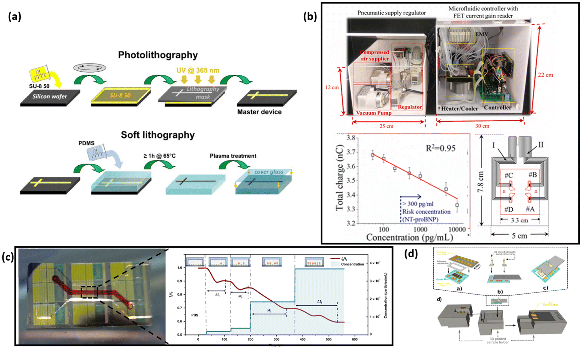 | ||
| Fig. 7 (a). Schematic of soft lithography-based fabrication of microfluidic channels.163 “Reproduced from ref. 163 with permission from The Royal Society of Chemistry, copyright 2013”. (b) Integrated FET sensor with microfluidic channels for automatic sampling and simultaneous detection of biomarkers for cardiovascular diseases.164 “Reproduced from ref. 164 with permission from Elsevier, copyright 2019”. (c) Microfluidic channel integration with silicon nanowire bio-FET for electrical and label-free detection of cancer cell-derived exosomes.46 “Reproduced from ref. 46 with permission from Springer Nature, Creative Commons Attribution (CC BY) license, copyright 2022”. (d). Microfluidic channel embedment for multi-gate detection of TNFα.165 “Reproduced from ref. 165 with permission from the American Chemical Society, CC-BY 4.0, copyright 2020”. | ||
Microfluidic platforms have been widely applied in biomedical engineering,166 chemistry,167,168 medicine,169,170 biology,171 and environmental science.172 The integration of a microfluidic system is a critical step in translating biosensors from laboratory research to real-world applications. Microfluidic technology allows for the incorporation of multiple functional modules into a compact device, enabling complex and precise fluid manipulations that achieve high sensitivities. The advantages of incorporating microfluidic platforms into biosensor systems include, but are not limited to: (1) enabling the detection of analytes in continuous flow and the simultaneous detection of multiple analytes; (2) streamlining complex assay protocols, such as mixing and washing; (3) minimizing sample volumes and reducing detection times, which further lowers costs when using expensive reagents; (4) providing a foundation for automated, high-throughput measurements and further integration of functions like sampling; (5) potentially enhancing the sensitivity by increasing the surface-to-volume ratio; and (6) miniaturizing the detection system for portability, disposability, and real-time detection.158,164,173–176 The high controllability and versatility offered by microfluidic channels make them a cornerstone for the development of next-generation POC biosensors.
Biosensors integrated with microfluidic channels can achieve automatic sample mixing and washing with minimum human operation. Sinha et al. demonstrated the design of a fully automated detection system based on FET biosensors integrated with microfluidic platforms for the detection of multiple cardiovascular biomarkers (Fig. 7b).164 In this system, all microfluidic control processes—including sample mixing and washing away excess materials—are programmed to ensure full automation. Since aptamers and ssDNA are used in the detection, both a heater and a cooler are required, which results in a size increase of the overall system. The entire automated system can be embedded in boxes measuring 25 cm × 12 cm × 15 cm and 55 cm × 25 cm × 22 cm. This research highlights the potential of microfluidic channel-integrated FET-based biosensor systems for fully automated detection. Zhao et al. also demonstrated that the integration of microfluidic channels allows for the functionalization of the sensing surface to occur simultaneously with the detection of analytes (Fig. 7c).46 Many FETs in laboratory settings utilize a drop-casting method to functionalize the sensor surface, which is crucial for enabling analyte binding and detection. However, this drop-casting method requires human intervention, which can hinder the full automation of systems. The introduction of microfluidic-based channels provides the basis for eliminating human intervention, allowing for fully automatic functionalization of the sensing surface and detection in one step. By removing the need for pre-functionalization, the shelf life of the biosensor can be significantly extended, broadening its potential applications.
Microfluidic channels have also been used as chambers for FET-based biosensors, which paves the way for simultaneous monitoring of multiple analytes with sensor arrays. While most organic electrolyte-gated FET reported in the literature are single-gated, Parkula et al. integrated OECTs with microfluidic channels and enabled the multi-gate detection of TNFα (Fig. 7d), achieving an LOD as low as 3 pM.165 A handheld device holder is designed using 3D printing technology to facilitate the easy installation and replacement of sensor chips, showcasing the potential of transistor-based biosensors for portable on-site detection applications. The ability to simultaneously detect multiple analytes, combined with the potential for full automation, positions the integration of microfluidic channels as a crucial component of biosensing platforms. The integrated biosensing platform can be further combined with advanced systems like samplers, smartphones and even cloud-AI analysis to enhance functionality and versatility. Microfluidic channels have also been effectively used to direct the sample solution to partly cover the channel material, which induces differences in electrical properties between the covered and uncovered areas. Tsang et al. demonstrated that using microfluidic channels to partly cover the graphene channels can induce an additional minimum alongside the original Dirac point of the graphene, enabling the sensitive detection of exosomes down to 0.1 μg mL−1 in 30 minutes.151
Several challenges arise in integrating microfluidic channels with FET-based biosensors, including miniaturization and packaging, material limitations, cost, device-to-device variation, and overcoming complexities in continuous flow detection.177–179 Miniaturization and packaging specifically refer to miniaturizing microfluidic platforms to a size that is compatible with biosensor chips and effectively packaging them onto the sensor. Currently, there is no standardized process for packaging microfluidic channels with biosensors. Device-to-device variation is another major concern, as consistency across different devices is difficult to achieve. Additionally, high fabrication costs further hinder the widespread adoption and commercialization of these biosensors. Recently, 3D printing has shown promise as a method for standardizing the fabrication of microfluidic systems, offering a potential solution to this problem.180,181 Material limitations also present challenges, particularly for application-specific uses. For instance, microfluidic channels designed for wearable devices must be fabricated from biocompatible materials to ensure safety when in contact with the human body.
When applying microfluidic-integrated FET sensors for sensing under physiological environments, such as for biomedically related applications, high-salt solutions can cause a screening effect known as Debye screening, which prevents the detection of analytes beyond the Debye length. The Debye screening length can be down to 1 nm in bio-fluid environments.182 For example, when detecting negatively charged molecules like streptavidin or DNA, the analytes become surrounded by positively charged ions from the high-salt solution due to electrostatic interaction. Beyond the Debye length, the number of surrounding positive charges approaches the number of negative charges on the analytes, effectively neutralizing the charge and preventing the FET from sensing any signal.183 The Debye length (λD) for aqueous solutions at room temperature can be calculated using the following eqn (4):
 | (4) |
The integration of microfluidic systems with biosensors enables the detection of analytes in a complex continuous flow. Since most biosensors are designed to detect analytes in a stagnant environment, overcoming the hydrodynamic forces that prevent analytes from binding to the sensing region becomes a major challenge in continuous flow applications, especially when particles are moving at high flow speeds. To address this, electrokinetic techniques such as AC electro-osmosis (EO) and dielectrophoresis (DEP) have been adopted for the separation of single cells within microfluidic channels.186 Han et al. demonstrated the use of combined AC-EO and DEP techniques to concentrate cells in a continuous flow, effectively overcoming the hydrodynamic forces and enhancing the detection efficiency of FET sensors.187 A 14.6-fold increase in fluorescent bead concentration was observed at the detection region using AC-EO and DEP combined techniques. Moreover, the system achieved an LOD of 150 CFU mL−1 for S. aureus in 0.01× PBS within 35 min, exhibiting high selectivity and specificity against S. epidermidis, E. coli, and B. subtilis.
Integration with samplers
Pathogen surveillance has become a critical focus, particularly following the outbreak of new epidemics. The recent SARS-CoV-2 pandemic reminds us that we are dramatically underestimating our vulnerability to pathogens and the importance of a rapid and accurate aerosol detection system for pathogenic organisms.188 In many countries, pathogen surveillance has been untimely and lagged behind the rapid spread of COVID-19. As a result, public health interventions like isolation, contact tracing, and quarantine were ineffectively coordinated to control the spread in the early stages.189 Studies investigating virus concentrations in both indoor and outdoor environments have consistently shown that crowded indoor spaces, such as airports and buses, exhibit significantly higher virus concentrations than outdoor settings.190–192 This finding underscores the importance of indoor monitoring over outdoor surveillance in open areas, particularly in densely populated environments. For example, Zhang et al. have conducted an environmental surveillance suggesting that approximately 100 more COVID-positive cases occurred during weeks with positive environmental samples compared with weeks without positive samples.190During the COVID-19 pandemic, nasal swab sampling followed by a PCR-based sequencing test was considered the gold standard for pathogen detection. However, this PCR-based method relies on benchtop sequencers in a laboratory setting, limiting its applicability for automated pathogen monitoring. Although some portable sequencers have been developed, their high cost hinders the establishment of a widespread automated pathogen monitoring network.193 Transistor-based biosensors hold tremendous potential for automated pathogen monitoring networks when integrated with automated samplers, owing to their electrical signal output, miniaturization potential, and suitability for mass production. With proper sampler integration, transistor-based biosensors can offer a highly competitive POC real-time detection method, as compared with the current PCR-based gold standard, which typically requires several hours to days to deliver results.
Automatic samplers offer a promising direction for enabling automatic sampling-to-detection applications, such as monitoring pathogen presence at specific locations. To establish an automated pathogen monitoring network in air, enabling automatic sampling of bioaerosols and converting them into liquid samples is a critical preparatory step. Conventional sampling methods include impaction, suction, electrostatic precipitation, filtration, and impingement (Fig. 8). In impaction methods, aerosol pathogens physically settle onto a solid surface, and adhesive-coated surfaces like petroleum jelly-coated surfaces are explored to enhance the passive impaction of aerosol pathogens.194,195 Although impaction is relatively inexpensive, it faces challenges in terms of efficiency and quantification. In contrast, impingement methods often use bubbling liquids to efficiently capture small pathogenic organisms and are more favoured in recent aerosol monitoring research.196,197 For example, researchers have employed liquid-phase samplers to collect airborne COVID-19 virus for subsequent PCR-based tests.190,198 However, challenges in impingement methods include small sample volumes and liquid loss due to evaporation. Filtration and suction methods can be combined, where a vacuum pump creates a pressure differential to accelerate airflow, and a filtration system collects pathogens of a specific size. This approach has been widely used with microfluidic channels to create an integrated sampling and detection system, although it suffers from lengthy operational processes such as transferring samples from a filter to microfluidic channels and culturing samples.199 The electrostatic precipitation methods utilize the natural charges of bacteria; e.g., most bacteria have a negative charge at neutral pH and an electropositive filter can be used to enhance pathogen capture.200 Each method presents unique advantages and challenges for integration into automated pathogen monitoring systems, and continued research is needed to improve the efficiency and scalability of these technologies.
 | ||
| Fig. 8 Schematic of common sampling-to-detection methods for bioaerosols. (a). Illustration of the autonomous pathogen detection system (APDS) developed in 2008 for environmental monitoring of biological threat agents.201 “Reproduced from ref. 201 with permission from the American Chemical Society, copyright 2008”. (b). Illustration of an automatic sample collection-to-detection biosensor system for Mycobacterium tuberculosis.202 “Reproduced from ref. 202 with permission from The Royal Society of Chemistry, copyright 2022”. (c). Cotton-tipped electrochemical immunosensor for sampling to detection of SARS-CoV-2.203 “Reproduced from ref. 203 with permission from the American Chemical Society, copyright 2021”. | ||
The real-time detection of infectious bioaerosols in the air with automated detection systems is particularly challenging due to several factors. First, the concentration of infectious pathogens in the air is extremely low, requiring highly efficient sampling methods to concentrate pathogens above the LOD for detection methods. Unfortunately, many available air samplers are not efficient enough at concentrating pathogens. Moreover, the loss of analytes due to the deterioration of aerosol pathogens during sampling—such as damage to antigen surface proteins or peptides—can significantly hinder detection capabilities. Factors like environmental stress, cell damage during sampling, and hydration all play important roles in the deterioration process of bio samples.197,204 Additionally, dust particles and biological contaminants like saliva or sputum in the air can interfere with sampler collection and biosensing methods. Dust particles, typically ranging from 1–100 nm in air, scatter light at different angles and intensities and can cause complications with optical-based biosensing methods, resulting in lowered sensitivity and specificity.199 Dust particles can also clog the air samplers, potentially leading to malfunction.205 To address these issues, parameters such as sampler location, filter size, sampling methods, and air flow rate need to be optimized in order to properly sample and concentrate the low-level pathogens in air for effective automated airborne bioaerosol detection.
An ideal integrated automatic biosensing platform should consist of both a highly efficient automated sampler and a highly sensitive portable diagnostic device. While there is extensive research on each component individually, studies focusing on the integration of these systems are comparatively fewer.206 The feasibility of integrating automatic samplers with various detection techniques has been reported. For example, in 2008, an Autonomous Pathogen Detection System (APDS) is first demonstrated and accepted by the US government (Fig. 8a), marking a significant advancement in this field. The APDS is capable of automatically collecting and selectively concentrating particles from the air into liquid samples, which are then analyzed using PCR-based methods within the system.201 The system utilizes a combination of filter screens and a wet-cyclone collector to convert airborne particles into liquid samples and has been successfully tested for detecting Bacillus anthracis and Yersinia pestis in both laboratories and high-traffic areas such as trains. Despite its potential, the overall size of the device is relatively bulky and its detection capability is affected by background noise from dust and other airborne particles. Lee et al. developed a lateral flow assay (LFA) based integrated system for bioaerosol sampling and monitoring, demonstrating a response to MS2 bacteriophage and avian influenza virus (AIV) H1N1 in a simulated environment.207 The system utilizes a porous glass fiber pad to capture pathogens from the inlet airflow, which are then flushed with buffers into the integrated LFA for detection. Near-infrared (NIR) emission is used as a signal to indicate the presence of pathogens and an LOD down to 106 PFU mL−1 is achieved for MS2 virus, which is 10-fold lower than that of commercial kits.
With the continued development of microfluidic channels and lab-on-a-chip technologies, FET-based devices have become promising candidates for POC automated airborne pathogen detection due to their miniaturization capabilities. Handheld signal readers can be used to read FET-based biosensor signals, unlike the bulkier readers required for optical- and PCR-based detection methods. Although the FET-based biosensors hold huge potential in the automated pathogen detection system, relatively little research has been conducted on integrating microfluidic-based FET sensing platforms with aerosol samplers for pathogen detection and monitoring. Ma et al. developed a Si-nanowire based FET biosensor integrated with samplers to detect Mycobacterium tuberculosis from patients’ exhalations (Fig. 8b).202 The sensor system collected a sufficient sample volume in less than 2 minutes and could detect MTB proteins in sputum-equivalent breath condensate (SEBC) at concentrations as low as 4 × 10⁴ particles per mL. The packaged sensor is flexible and portable with a size of 36 mm by 31 mm. Similarly, Lee et al. designed a CNT-based FET that is able to detect two different kinds of airborne allergic fungal particle simultaneously.208 The CNT-based FET was integrated with a commercial air-to-liquid sampler through a predesigned microfluidic channel to achieve automated sampling and detection. The system successfully detected Alternaria alternata and Aspergillus niger in the range of 10–106 pg mL−1. In addition, a Peltier cooler was incorporated to enhance the receptor stability, extending the sensor shelf-life up to 9 days.
Beyond the traditional approach of connecting an external sampler to the sensing device, sampling may be merged with sensing on the same chip, creating a self-diagnostic kit. Eissa et al. fabricated an electrochemical biosensor for COVID-19 detection using screen-printing technology (Fig. 8c). In this design, cotton fibers were incorporated onto the detection zone of the electrode to enable same-chip sampling and detection. The immunosensor was fabricated by immobilizing the virus antigen on CNF-modified screen-printed electrodes, and the detection of virus antigen was achieved via competitive assay. After sampling the nasal samples, the chip is immersed into PCR tubes containing a fixed amount of N protein antibodies in the solution; typically, a higher concentration of virus in the sample results in fewer antibodies binding to the sensor surface. The impact of cotton on the signal was found to be insignificant through comparison experiments.203 Considering the advancements in this field, integrating FET biosensors with samplers for automated detection holds great promise. The continued development of these technologies could lead to a new generation of POC biosensors with wide applications for real-time, automated pathogen detection.
Integration with wearable devices
Wearable designs can be incorporated with transistor biosensors for everyday healthcare, assisting patients in monitoring critical biological entities. The popularity of wearable devices has surged with the advancement of smartphones and the IoT. To date, biosensors have been incorporated into a wide range of wearable devices, including clothing, bandages, rings, masks, tattoos, and contact lenses.209Wearable devices can be classified into two categories: casual use and medical-care specific. Casual wearables, such as the Apple watch, are primarily designed to track physical activity and fitness, often serving as both a health tool and an entertainment device. On the other hand, medical-care-specific wearable devices are developed to monitor specific physiological parameters and provide critical health insights. These devices can be worn on the skin or specific locations on the body; for example, some continuous glucose monitors require the insertion of a sensor pellet under the skin of upper arm. Medical care-type wearable devices, such as glucose monitors, provide continuous monitoring of specific physiological activities on a hourly basis, daily basis, or weekly basis and may require replacement after certain periods of time.210
Key considerations for the development of excellent wearable devices include miniaturization, efficient sampling methods, biocompatibility, flexibility, and reliable performance under various bending conditions. Currently studies on wearable devices are largely focused on non-invasive, dynamic monitoring of health through biofluids such as interstitial fluid, saliva, tear, and sweat.209 The applications of wearable devices require them to be lightweight and user-friendly to ensure ease of use and acceptance by end-users.
Saliva is an oral biofluid containing a variety of components such as metabolites, hormones, enzymes, microorganisms, proteins, and ions that permeate from blood via transcellular or paracellular paths.211 Since saliva is more readily available compared with blood, it is an excellent non-invasive medium for monitoring the emotional, hormonal, nutritional, and metabolic state of the human body.212 Saliva can be sampled onto the sensing device either through passive drooling or with the aid of a swab.213,214 Klinghammer et al. demonstrated a multiplexed platform comprising an array of SiNW FET sensors for label-free monitoring of the stress biomarker cortisol in saliva.215 The sensor employed an aptamer probe for the detection and utilized the folding of the aptamer upon binding, close to the sensor surface, to overcome the Debye length limitations. Additionally, Li et al. developed a PEDOT-based electrochemical biosensor for at-home, centrifuge-free testing of the female ovarian hormone cycle, specifically detecting both progesterone (P4) and estradiol (E2) (Fig. 9a). The 3D micropyramidal arrays fabricated on the PEDOT surface were reported to significantly enhance the sensitivity of the sensor, achieving detection at sub-femtomolar (sub-fM) levels.216
 | ||
| Fig. 9 (a). Tip-enhanced sub-femtomolar salivary immunosensor for steroid sex hormones.216 “Reproduced from ref. 216 with permission from the American Chemical Society, copyright 2023”. (b). Wearable smart sensor system integrated on soft contact lenses for wireless ocular diagnostics.217 “Reproduced from ref. 217 with permission from Springer Nature, Creative Commons Attribution (CC BY) license, copyright 2017”. (c). Ultra-low-volume lab-on-skin passive microfluidics embedded ion-sensitive field-effect transistor for ion detection in sweat.218 “Reproduced from ref. 218 with permission from the American Chemical Society, copyright 2018”. (d). Schematics of potential biosensor integration with the IoT.219 “Reproduced from ref. 219 with permission from Elsevier, copyright 2020”. | ||
Tears are a complex extracellular fluid consisting of proteins, electrolytes, peptides, lipids, and metabolites from various sources including the lacrimal glands, goblet cells, epithelial cells and blood.209 Since blood is one of the contributors to tears, tears can be used to monitor the glucose levels in diabetic patients. However, two main challenges hinder tear-based detection. First, in bench-top detection, the transportation of the tear sample to the lab can lead to evaporation which considerably affects the detection accuracy. Second, sampling tears from delicate human eyes poses a significant challenge and requires extreme caution. Given these challenges, smart contact lenses have emerged as a promising candidate for real-time monitoring of parameters such as glucose level, intraocular pressure, and pH.220 Park et al. demonstrated FET-based soft contact lenses for glucose monitoring, using pyrene linker-aided glucose oxidase probes immobilized on the graphene surface (Fig. 9b).217 The soft contact lens has been tested both in vivo and in vitro using live rabbit and bovine eyeballs, demonstrating reliable operation with an LOD down to 0.4 × 10⁻⁶ M.
Up to 30% of bodily waste is secreted through perspiration from the sweat glands in the human skin during daily exercise. Sweat contains a variety of chemicals, including ions, metabolites, acids, hormones, small proteins, and peptides, offering abundant information on people's health status.221 Given its rich composition, sweat can be used to monitor physiological conditions such as intoxication levels and drug abuse.222,223 With the recent advancements in wearable autonomous collection platforms, it is possible to achieve non-invasive collection and real-time analysis of sweat directly from the skin. Wang et al. demonstrated a wearable non-invasive biosensor for continuous monitoring of essential amino acids and vitamins in sweat during exercise and at rest.224 The incorporation of carbachol hydrogel at the anode and cathode facilitates efficient microfluidic-based sweat sampling, enabling autonomous and continuous sweat monitoring with high accuracy across activities including physical exercise and at rest.
Skin interstitial fluid (ISF), which surrounds cells and can be collected through diffusion, plays a crucial role in delivering nutrients and removing waste via the blood capillaries. This fluid contains a wealth of vital information, making it an excellent medium for continuous health assessments. Detection of glucose levels through interstitial fluid has been an extensive focus over the past several decades. Various biosensors based on Raman spectroscopy, photoacoustic spectroscopy, electromagnetic waves, and FET have been developed for glucose monitoring.225 Some ISF biosensors utilize microneedles for sampling,226,227 while many commercial glucose sensors utilize non-invasive iontophoresis-based techniques, such as the GlucoWatch®, GlucoTrack™, G2 Biographer device and OrSense NBM-200G,209,228 offering a more convenient and less painful alternative for patients.
One important integration for wearable devices is the incorporation of microfluidic channels for automated, passive biofluid collection. Zou et al. demonstrated a microfluidic channel integrated extended-gate FET-based sensor for pH detection.181 The fluid inlet in the microfluidic channel is driven by a capillary flow pump, enabling body fluid collection during wearing. Additionally, a temperature detection pad was incorporated into the sensor for temperature compensation, with measurement results showing a deviation of only 0.17 °C from the gold standard. The microfluidic channel can be fabricated cost-effectively using 3D printing, achieving a 200 μm accuracy with a printing time of less than 10 minutes, highlighting the potential for mass production. Similarly, Garcia-Cordero et al. developed an ion-sensitive lab-on-skin biosensor which can passively collect sweat from a person's skin via capillary forces, allowing for the detection of pH levels and concentrations of Na+ and K+ ions (Fig. 9c).218
Compared with traditional POC sensors, wearable devices are designed to be worn on the wrist or other body parts, requiring flexibility to fit closely on various skin surfaces for efficient biofluid collection. This translates into a unique demand for wearable sensors that traditional FET-based POC devices do not face: high endurance toward bending cycles and the ability to maintain consistent performance under various curvatures. E. Laliberte et al. developed a wearable graphene-based FET on 50 nm SiO2-coated flexible Kapton film that addresses these challenges. The wearable device achieves a detection range of 10 pM to 100 nM for interleukin-6 (IL-6) protein, a key biomarker in immune responses. The wearable biosensors can withstand a 1.5 cm to 4.25 cm radius of curvature while maintaining proper functionality. The wearable biosensor is also integrated with a microfluidic channel and a specially designed portable signal meter, allowing for real-time, dynamic monitoring of IL-6 with portable readouts.229 While organic soft materials are often preferred for their flexibility, research has shown that inorganic materials such as graphene and indium oxide can also be used to fabricate highly flexible biosensors with minimal performance loss during bending cycles.230 For example, Chen et al. demonstrated polymer-based OECT that maintained stable electrochemical properties over 1500 redox cycles under 104 stretching cycles of 30% strain.231
Wearable devices, as their name implies, require direct contact with the skin, necessitating the use of biocompatible materials to ensure the safety and comfort of the wearer. In the future, wearable devices are expected to evolve into implantable sensors for more precise monitoring, especially for patients with high-risk conditions. In terms of biocompatibility, most metal-based materials such as Ag, Cu, and Al are not ideal for biosensors as these metals can penetrate body tissue after prolonged skin contact, posing potential health risks232 In contrast, inert metals like gold (Au), platinum (Pt), and titanium (Ti), along with carbon-based and ceramic composite materials, offer better biocompatibility and are potential candidates for wearable biosensors. Organic materials, however, provide an even broader range of options, such as PEDOT:PSS and hydrogel materials, offering the flexibility to meet specific functional requirements. Lots of different OECTs have been developed for wearable applications. For example, J. Currano et al. developed a PEDOT:PSS-based sensor pad on a Kapton substrate that can successfully detect lactate in sweat, exhibiting an electrical sensitivity of 1.9 mA mM−1.233 Fumeaux et al. designed a disposable, biocompatible OECT made from polylactic acid (PLA), carbon, PEDOT:PSS, and PMMA. The device has carbon and PEDOT:PSS printed on top of the PLA substrate as electrodes and gate, respectively, and PMMA-based microfluidic channels fabricated on top of the devices. The sensor demonstrated linear detection for glucose up to 1 mM, showcasing the potential of these materials for wearable, non-invasive health monitoring.234
Several challenges remain in the translation of wearable devices for real-world applications, including standardization of the fabrication process, ensuring device stretchability, efficient sample detection, and extending shelf life.235 The standardization of the fabrication process has been a long-standing issue for nearly all transistor-based biosensors, not just wearable devices. Current issues such as device-to-device variation, low device yield, and inconsistent surface functionalization fall short of meeting commercial requirements. In terms of stretchability, while numerous studies have demonstrated flexible wearable biosensors that can maintain performance under laboratory bending tests, real-world applications are far more complex, involving forces such as buckling, shear, and compression, which affect device durability and functionality. Similarly, while many laboratory sensor devices have shown the ability to automatically collect biofluids like sweat, real-life conditions introduce additional complications such as dirt, dust, and small particles that can clog microfluidic channels, potentially impairing functionality. Shelf life presents another significant challenge for wearable devices. Depending on the specific applications, users’ tolerance for the price and device longevity varies. For example, patients with diabetes might be willing to pay for a wearable device that needs to be replaced every one or two weeks if it can accurately detect glucose levels, as it is crucial for them. However, for most people looking to monitor their health for general wellness purposes, a device with less than one month of shelf life may not be an appealing choice for them. To enable the real-life translation of transistor-based wearable devices, extensive testing and optimization are required to overcome these challenges.
Integration with the Internet of Things (IoT)
Sensors can be further integrated with smartphones or the IoT to enable wireless communication, extending their functionality to even form large sensor networks capable of acting as an “electronic nose” for automatically monitoring harmful molecules and pathogens over large areas. In the past decades, with the rapid development of artificial intelligence (AI), the IoT has become a powerful technology that seamlessly integrates with various electronic devices to support everyday life. The intelligent processing of biosensing data is revolutionary for applications in healthcare and public health. In the realm of public health, AI-integrated biosensors can establish large areas of sensor networks to monitor the outbreak or transmission of certain diseases, allowing governments and health authorities to take timely control. In personal healthcare, AI-integrated biosensors can enable one medical team to monitor the health conditions of a large number of patients, allowing for prompt interventions when abnormal health patterns are detected. Furthermore, individuals could remotely monitor the health of elderly family members or patients with chronic diseases, offering increased flexibility and convenience in caregiving. There is no doubt that the future of biosensing will be shaped by the integration of smart technologies—ushering in an era of intelligence.The basic architecture of AI-biosensors is composed of three main elements: information collector, signal transducer, and cloud data processing (Fig. 9d).219 The information collector refers to the integration of biosensors with samplers, microfluidic channels, or wearable devices. These integrations enable the collection of target biomolecules from various sources, such as body fluids or environmental samples. The signal transducer refers to the component of the biosensor responsible for converting the presence or concentration of biomolecules into electrical signals. The last part, cloud data processing, refers to the processing and analysis of electrical signals with AI techniques. The data undergoes classification, modelling, and analysis, allowing for advanced pattern recognition and decision-making.
The three-part architecture offers a comprehensive framework for understanding the biosensor translation process. The signal transducer part represents the development of biosensors in the laboratory, where the primary focus is on optimizing the performance of the sensor itself. Key objectives in this phase include achieving a lower limit of detection, expanding the sensing range, enhancing selectivity, and simplifying the sensing process. This phase defines the technical capabilities of the biosensor. The information collector part can be analogous to the front end of the biosensor system, where the ultimate goal is to develop innovative methods to automatically collect and process the sample in real-time. This stage ensures that the biosensor can seamlessly interact with the environment to effectively capture analytes with minimal human intervention. The last, cloud data-processing, part is the step for the translation of biosensors into real healthcare solutions. Biosensors equipped with integrated information collectors alone are considered as semi-finished products. It is only through further integration with cloud data analysis that biosensors can evolve into next-generation healthcare tools.
Given the popularity of smartphones in this era, the integration of smartphone technology for biosensor actuation and monitoring has garnered significant attention. Smartphones can be directly or wirelessly connected to electronic analyzers and sensor chips for the detection of specific biomolecules, offering a convenient and user-friendly platform for real-time monitoring. For example, Zhao et al. has developed an ultrasensitive electrochemical sensor targeting the RNA of SARS-CoV-2 using calixarene-functionalized graphene oxide. The device eliminates the need for specific nucleic acid amplification and is directly connected to smartphones.236 Similarly, Su et al. demonstrated the use of smartphones as wireless data acceptors for the detection of serum-derived exosomes and secretion monitoring.237
Another emerging field is the integration of machine learning (ML) with biosensors. ML enhances data analysis by extracting more meaningful information from raw sensor data. Its applications include: (1) categorizing the sensing signal into various groups through algorithms based on different analytes, (2) reducing background noise during detection, such as sensor internal drifts, contaminations, and environmental fluctuations, (3) ruling out abnormal signals to improve the accuracy of detection, and (4) identifying patterns and signals that might be overlooked by human analysis.238 For example, using ML trained from multi-dimensional information collected through multi-sensor arrays, Xue et al. demonstrated improved system functionality and accuracy for multipleion detection in complex solutions.239 By employing a random forest algorithm, their system accurately classified ion types, predicted ion concentrations, and analyzed electrolyte imbalances related to diseases.226
Another key integration involves wireless data transmission and the formation of sensor networks. This idea is similar to the real-time continuous soil monitoring networks.240 The integration of wireless data transmission, sensor network, and AI analysis represents the next frontier for biosensors in real-life applications. Biosensors could form vast sensor networks where each node is a portable biosensor that autonomously samples and detects bioaerosols in the air. Data from these nodes can be wirelessly transmitted to the cloud for machine learning analysis, facilitating timely responses by governments. Biosensors can also be deployed in retirement communities and disseminated to each resident to help doctors quickly respond to emergencies experienced by residents. As biosensing and AI technologies continue to evolve, the applications of these integrated platforms will expand significantly, broadening their impact on public health and personalized healthcare.
4. Conclusions and outlook
Biosensors are expected to become a central focus in the coming decades due to their close connection to public and personal health. Transistor-based biosensors are especially promising candidates among the various types of biosensor, given their portability, sensitivity, and accuracy. Additive manufacturing presents a significant advantage for the mass fabrication of transistor biosensors with minimum sample load, drop-on-demand deposition, and customizability. However, several challenges remain, such as the need for higher printing precision and potential clogging of the nozzle, which affects almost all printing methods. Compared with conventional fabrication techniques like CVD and drop casting, additive manufacturing acts as a balanced choice for depositing nanomaterials—producing a high-quality film with a controllable thickness both time- and cost-efficiently. It is anticipated that advanced printing techniques will become important fabrication methods in the future for not only laboratory production but also the mass production of high-quality transistor-based biosensors. The development of 3D printing technology may enable onsite sensor production according to demand, which would be extremely valued in remote rural area or countries with limited transportation and harsh storage environments. The ability to fabricate sensors onsite based on immediate needs also addresses concerns about sensor shelf-life and transportation logistics.For promising laboratory-developed devices, it is important to translate them into real-world applications. The first step of translation is the integration with lab-on-a-chip and microfluidic platforms. The lab-on-a-chip integration prepares the biosensors for mass-production, while also enhancing the portability of biosensors for various applications. Integration with microfluidic platforms enables the detection of various biomolecules in dynamic environments, such as continuous flow systems, and builds the cornerstone for further functionality. Some of these further functionalities could include the integration of samplers to improve information collection such as autonomous samplers for large-area monitoring and wearable devices for personal healthcare. Another further functionality is improving the wireless communication and data analysis ability through integration with the IoT. Cost-effective wireless sensors could also be deployed in networks to remotely monitor the presence of hazardous bioaerosols in large areas and help governments to take timely control of any outbreak of epidemic.
For successful commercialization of transistor-based biosensors, it is essential for these sensors to differentiate themselves not only through performance—sensitivity and selectivity—but also through device integrations, such as wearability, IoT capabilities, and user interfaces (UIs). As more research begins to focus on the functional integration of devices for transistor-based biosensors, alongside advances in nanomaterials and structures, the translation of these biosensors into practical applications is expected to accelerate in the coming years. Despite research being conducted over the past decades on transistor-based biosensors, this type of sensor is still considered relatively new to the market. Regulatory approvals and clinical validations present significant hurdles that must be overcome before translating these technologies into commercial products. Regulatory agencies classify biosensors as medical devices, necessitating stringent validation before they can be marketed. Transistor-based biosensors for POC diagnostics, disease detection and biomarker monitoring fall under moderate to high-risk categories, demanding extensive tests and approval processes. As emerging technologies, transistor-based biosensors face the challenge of establishing global regulatory standards and integrating with existing diagnostic standards. Clinical validation is essential for demonstrating the effectiveness of these biosensors in complex real-world diagnostic environments, typically involving multiple testing phases, such as laboratory-based analytical validation, preclinical testing, and clinical trials. This entire validation process can take years to complete, which is why transistor-based biosensors are still progressing toward commercialization. While few FET-based sensors have been commercialized, Sentron has successfully introduced an ion-sensitive field-effect transistor (ISFET) for pH detection.241 Similarly, Paragraf has commercialized a graphene FET for both potassium and pH detection.242 A notable FET biosensor nearing commercialization is being developed by QuLab Medical, a medical device and digital health startup, which announced in 2023 a new multi-metabolite wearable sensor for type I diabetes (T1D) management based on its patented FET sensors.243,244 Despite these challenges, transistor-based biosensors, with their portability, sensitivity, and potential for integration, will likely play an important role in the next era in fields such as personalized healthcare, environmental monitoring, smart cities, and infrastructure management, as challenges related to shelf life, yield, cost, regulatory approvals, and clinical validations continue to be addressed.
Data availability
No primary research results, software or code have been included and no new data were generated or analysed as part of this review.Conflicts of interest
There are no conflicts to declare.Acknowledgements
J. H. Chen acknowledges the financial support from the US National Science Foundation (NSF) PIPP Program (NSF 2200234) and the NSF Future Manufacturing Program (NSF 2037026).References
- E. Valera, A. Jankelow, J. Lim, V. Kindratenko, A. Ganguli, K. White, J. Kumar and R. Bashir, ACS Nano, 2021, 15, 7899–7906 CrossRef PubMed.
- The top 10 causes of death, https://www.who.int/news-room/fact-sheets/detail/the-top-10-causes-of-death, (accessed December 25, 2023).
- COVID-19 deaths | WHO COVID-19 dashboard, https://data.who.int/dashboards/covid19/cases, (accessed December 25, 2023).
- S. Samota, R. Rani, S. Chakraverty and A. Kaushik, Mater. Sci. Semicond. Process., 2022, 141, 106404 CrossRef.
- M. Sharafeldin and J. J. Davis, Anal. Chem., 2021, 93, 184–197 Search PubMed.
- X. Zhang, Y. Shi, G. Chen, D. Wu, Y. Wu and G. Li, Small Methods, 2022, 6, 2200794 Search PubMed.
- Point of Care Tests, https://www.who.int/teams/sexual-and-reproductive-health-and-research-(srh)/areas-of-work/sexual-health/sexually-transmitted-infections/point-of-care-tests, (accessed January 17, 2023).
- WHO launches global network to detect and prevent infectious disease threats, https://www.who.int/news/item/20-05-2023-who-launches-global-network-to–detect-and-prevent-infectious-disease-threats, (accessed December 25, 2023).
- A. Silvestri, J. Zayas-Arrabal, M. Vera-Hidalgo, D. D. Silvio, C. Wetzl, M. Martinez-Moro, A. Zurutuza, E. Torres, A. Centeno, A. Maestre, J. M. Gómez, M. Arrastua, M. Elicegui, N. Ontoso, M. Prato, I. Coluzza and A. Criado, Nanoscale, 2023, 15, 1076–1085 Search PubMed.
- G. Seo, G. Lee, M. J. Kim, S.-H. Baek, M. Choi, K. B. Ku, C.-S. Lee, S. Jun, D. Park, H. G. Kim, S.-J. Kim, J.-O. Lee, B. T. Kim, E. C. Park and S. I. Kim, ACS Nano, 2020, 14, 5135–5142 Search PubMed.
- M. T. Hwang, M. Heiranian, Y. Kim, S. You, J. Leem, A. Taqieddin, V. Faramarzi, Y. Jing, I. Park, A. M. van der Zande, S. Nam, N. R. Aluru and R. Bashir, Nat. Commun., 2020, 11, 1543 CAS.
- K. Guo, S. Wustoni, A. Koklu, E. Díaz-Galicia, M. Moser, A. Hama, A. A. Alqahtani, A. N. Ahmad, F. S. Alhamlan, M. Shuaib, A. Pain, I. McCulloch, S. T. Arold, R. Grünberg and S. Inal, Nat. Biomed. Eng., 2021, 5, 666–677 CAS.
- M. Eswaran, B. Chokkiah, S. Pandit, S. Rahimi, R. Dhanusuraman, M. Aleem and I. Mijakovic, Small Methods, 2022, 6, 2200809 CrossRef CAS.
- P. Sadeghi, H. Sohrabi, M. Hejazi, A. Jahanban-Esfahlan, B. Baradaran, M. Tohidast, M. R. Majidi, A. Mokhtarzadeh, S. M. Tavangar and M. de la Guardia, TrAC, Trends Anal. Chem., 2021, 145, 116460 CrossRef CAS PubMed.
- S. Sakamoto, W. Putalun, S. Vimolmangkang, W. Phoolcharoen, Y. Shoyama, H. Tanaka and S. Morimoto, J. Nat. Med., 2018, 72, 32–42 CrossRef CAS PubMed.
- P. Damborský, J. Švitel and J. Katrlík, Essays Biochem., 2016, 60, 91–100 Search PubMed.
- Y.-T. Chen, Y.-C. Lee, Y.-H. Lai, J.-C. Lim, N.-T. Huang, C.-T. Lin and J.-J. Huang, Biosensors, 2020, 10, 209 CrossRef PubMed.
- M. H. Pourasl, A. Vahedi, H. Tajalli, B. Khalilzadeh and F. Bayat, Sci. Rep., 2023, 13, 6847 CrossRef PubMed.
- S. M. Borisov and O. S. Wolfbeis, Chem. Rev., 2008, 108, 423–461 CrossRef PubMed.
- A. Uniyal, G. Srivastava, A. Pal, S. Taya and A. Muduli, Plasmonics, 2023, 18, 735–750 CrossRef.
- Y. Nasu, C. Murphy-Royal, Y. Wen, J. N. Haidey, R. S. Molina, A. Aggarwal, S. Zhang, Y. Kamijo, M.-E. Paquet, K. Podgorski, M. Drobizhev, J. S. Bains, M. J. Lemieux, G. R. Gordon and R. E. Campbell, Nat. Commun., 2021, 12, 7058 CrossRef.
- J. A. Huffman, A. E. Perring, N. J. Savage, B. Clot, B. Crouzy, F. Tummon, O. Shoshanim, B. Damit, J. Schneider, V. Sivaprakasam, M. A. Zawadowicz, I. Crawford, M. Gallagher, D. Topping, D. C. Doughty, S. C. Hill and Y. Pan, Aerosol Sci. Technol., 2020, 54, 465–495 CrossRef.
- J. Baranwal, B. Barse, G. Gatto, G. Broncova and A. Kumar, Chemosensors, 2022, 10, 363 Search PubMed.
- J. Fan, S. Parr, S. Kang and M. Gupta, Nanoscale, 2023, 15, 5476–5485 RSC.
- D. Sadighbayan, M. Hasanzadeh and E. Ghafar-Zadeh, TrAC, Trends Anal. Chem., 2020, 133, 116067 CrossRef.
- M. Chhowalla, D. Jena and H. Zhang, Nat. Rev. Mater., 2016, 1, 1–15 Search PubMed.
- R. A. Picca, K. Manoli, E. Macchia, L. Sarcina, C. Di Franco, N. Cioffi, D. Blasi, R. Österbacka, F. Torricelli, G. Scamarcio and L. Torsi, Adv. Funct. Mater., 2020, 30, 1904513 Search PubMed.
- P. Li and T. Lei, J. Polym. Sci., 2022, 60, 377–392 CrossRef.
- B. G. Sonmez, O. Ertop and S. Mutlu, Sci. Rep., 2017, 7, 12190 CrossRef PubMed.
- J. Jiang, J. Li, Y. Li, J. Duan, L. Li, Y. Tian, Z. Zong, H. Zheng, X. Feng, Q. Li, H. Liu, Y. Zhang, T.-L. Ren and L. Han, npj 2D Mater. Appl., 2019, 3, 1–8 CrossRef.
- M. S. Fuhrer and J. Hone, Nat. Nanotechnol., 2013, 8, 146–147 Search PubMed.
- Y. Niu, Z. Qin, Y. Zhang, C. Chen, S. Liu and H. Chen, Mater. Futures, 2023, 2, 042401 CrossRef.
- D. Majak, J. Fan and M. Gupta, Sens. Actuators, B, 2019, 286, 111–118 Search PubMed.
- N. Wang, Y. Liu, Y. Fu and F. Yan, ACS Appl. Mater. Interfaces, 2018, 10, 25834–25840 Search PubMed.
- E. Macchia, P. Romele, K. Manoli, M. Ghittorelli, M. Magliulo, Z. M. Kovács-Vajna, F. Torricelli and L. Torsi, Flexible Printed Electron., 2018, 3, 034002 Search PubMed.
- J. Yu, A. Yang, N. Wang, H. Ling, J. Song, X. Chen, Y. Lian, Z. Zhang, F. Yan and M. Gu, Nanoscale, 2021, 13, 2868–2874 Search PubMed.
- M. Jeyavelan, K. Khurshid, M. Akhil, R. R. Kannan, A. Ramesh, S. Nagarajan, M. Hofmann and M. S. L Hudson, Biosens. Bioelectron.: X, 2022, 12, 100251 Search PubMed.
- H. Chen, M. Xiao, J. He, Y. Zhang, Y. Liang, H. Liu and Z. Zhang, ACS Sens., 2022, 7, 2075–2083 Search PubMed.
- S. Wang, M. Sun, Y. Zhang, H. Ji, J. Gao, S. Song, J. Sun, H. Liu, Y. Zhang and L. Han, Anal. Chem., 2022, 94, 14785–14793 Search PubMed.
- A. Wasfi, F. Awwad, N. Qamhieh, B. Al Murshidi, A. R. Palakkott and J. G. Gelovani, Sci. Rep., 2022, 12, 18155 Search PubMed.
- M. Moser, T. C. Hidalgo, J. Surgailis, J. Gladisch, S. Ghosh, R. Sheelamanthula, Q. Thiburce, A. Giovannitti, A. Salleo, N. Gasparini, A. Wadsworth, I. Zozoulenko, M. Berggren, E. Stavrinidou, S. Inal and I. McCulloch, Adv. Mater., 2020, 32, 2002748 Search PubMed.
- D.-J. Kim, N.-E. Lee, J.-S. Park, I.-J. Park, J.-G. Kim and H. J. Cho, Biosens. Bioelectron., 2010, 25, 2477–2482 Search PubMed.
- B. Thakur, G. Zhou, J. Chang, H. Pu, B. Jin, X. Sui, X. Yuan, C.-H. Yang, M. Magruder and J. Chen, Biosens. Bioelectron., 2018, 110, 16–22 Search PubMed.
- Y. Chen, R. Ren, H. Pu, X. Guo, J. Chang, G. Zhou, S. Mao, M. Kron and J. Chen, Sci. Rep., 2017, 7, 10974 CrossRef PubMed.
- H. Liu, A. Yang, J. Song, N. Wang, P. Lam, Y. Li, H. K. Law and F. Yan, Sci. Adv., 2021, 7, eabg8387 CrossRef PubMed.
- W. Zhao, J. Hu, J. Liu, X. Li, S. Sun, X. Luan, Y. Zhao, S. Wei, M. Li, Q. Zhang and C. Huang, Microsyst. Nanoeng., 2022, 8, 1–12 CrossRef PubMed.
- H. S. Magar, R. Y. A. Hassan and M. N. Abbas, Sci. Rep., 2023, 13, 2034 CrossRef.
- R. Hajian, S. Balderston, T. Tran, T. deBoer, J. Etienne, M. Sandhu, N. A. Wauford, J.-Y. Chung, J. Nokes, M. Athaiya, J. Paredes, R. Peytavi, B. Goldsmith, N. Murthy, I. M. Conboy and K. Aran, Nat. Biomed. Eng., 2019, 3, 427–437 Search PubMed.
- H. K. Yu, K. Balasubramanian, K. Kim, J.-L. Lee, M. Maiti, C. Ropers, J. Krieg, K. Kern and A. M. Wodtke, ACS Nano, 2014, 8, 8636–8643 Search PubMed.
- S. Razza, S. Castro-Hermosa, A. Di Carlo and T. M. Brown, APL Mater., 2016, 4, 091508 Search PubMed.
- Y. Xiang, K. Miller, J. Guan, W. Kiratitanaporn, M. Tang and S. Chen, Arch. Toxicol., 2022, 96, 691–710 Search PubMed.
- J. A. Hondred, L. R. Stromberg, C. L. Mosher and J. C. Claussen, ACS Nano, 2017, 11, 9836–9845 CrossRef PubMed.
- W. J. Hyun, E. B. Secor, M. C. Hersam, C. D. Frisbie and L. F. Francis, Adv. Mater., 2015, 27, 109–115 Search PubMed.
- B. Chen, M. Kruse, B. Xu, R. Tutika, W. Zheng, M. D. Bartlett, Y. Wu and J. C. Claussen, Nanoscale, 2019, 11, 5222–5230 RSC.
- W. Honda, S. Harada, T. Arie, S. Akita and K. Takei, Adv. Funct. Mater., 2014, 24, 3299–3304 CrossRef.
- R. F. Hossain, I. G. Deaguero, T. Boland and A. B. Kaul, npj 2D Mater. Appl., 2017, 1, 1–10 CrossRef.
- M. Massetti, S. Zhang, P. C. Harikesh, B. Burtscher, C. Diacci, D. T. Simon, X. Liu, M. Fahlman, D. Tu, M. Berggren and S. Fabiano, npj Flexible Electron., 2023, 7, 1–11 Search PubMed.
- Q. Sun, C. Ma, W. Li, X. Li, K. Sakamoto, X. Liu, A. Okamoto and T. Minari, ACS Appl. Electron. Mater., 2023, 5, 2558–2565 CrossRef.
- R. Cao, X. Pu, X. Du, W. Yang, J. Wang, H. Guo, S. Zhao, Z. Yuan, C. Zhang, C. Li and Z. L. Wang, ACS Nano, 2018, 12, 5190–5196 CrossRef PubMed.
- C. Cao, J. B. Andrews and A. D. Franklin, Adv. Electron. Mater., 2017, 3, 1700057 CrossRef.
- E. Bihar, S. Wustoni, A. M. Pappa, K. N. Salama, D. Baran and S. Inal, npj Flexible Electron., 2018, 2, 1–8 CrossRef.
- A. E. Alexander, N. Wake, L. Chepelev, P. Brantner, J. Ryan and K. C. Wang, J. 3D Print. Med., 2021, 7, 8 Search PubMed.
- C. W. Hull, Apparatus for production of three-dimensional objects by stereolithography, US Pat., 638905, 1984 Search PubMed.
- C. M. B Ho, S. H. Ng, K.H.H. Li and Y. J. Yoon, Lab Chip, 2015, 15, 3627–3637 Search PubMed.
- B. C. Gross, J. L. Erkal, S. Y. Lockwood, C. Chen and D. M. Spence, Anal. Chem., 2014, 86, 3240–3253 CrossRef PubMed.
- J. F. Rusling, ACS Sens., 2018, 3, 522–526 Search PubMed.
- C. W. Foster, R. O. Kadara and C. E. Banks, in Screen-Printing Electrochemical Architectures, ed. C. E. Banks, C. W. Foster and R. O. Kadara, Springer International Publishing, Cham, 2016, pp. 1–12 Search PubMed.
- N. Kapur, S. J. Abbott, E. D. Dolden and P. H. Gaskell, IEEE Trans. Compon., Packag., Manuf. Technol., 2013, 3, 508–515 Search PubMed.
- N. Zavanelli and W.-H. Yeo, ACS Omega, 2021, 6, 9344–9351 Search PubMed.
- J. Liang, K. Tong and Q. Pei, Adv. Mater., 2016, 28, 5986–5996 CrossRef PubMed.
- K. Sinha, A. Chakraborty, Z. Ahmed, P. Mukherjee, P. Dutta, C. Das Mukhopadhyay and C. RoyChaudhuri, ACS Biomater. Sci. Eng., 2023, 9, 5886–5899 CrossRef PubMed.
- M. Zabihipour, R. Lassnig, J. Strandberg, M. Berggren, S. Fabiano, I. Engquist and P. Andersson Ersman, npj Flexible Electron., 2020, 4, 1–8 CrossRef.
- A. G.-M. Ferrari, S. J. Rowley-Neale and C. E. Banks, Talanta Open, 2021, 3, 100032 Search PubMed.
- C.-F. Wang, X.-Y. Sun, M. Su, Y.-P. Wang and Y.-K. Lv, Analyst, 2020, 145, 1550–1562 Search PubMed.
- J. R. Sempionatto, L. C. Brazaca, L. García-Carmona, G. Bolat, A. S. Campbell, A. Martin, G. Tang, R. Shah, R. K. Mishra, J. Kim, V. Zucolotto, A. Escarpa and J. Wang, Biosens. Bioelectron., 2019, 137, 161–170 CrossRef PubMed.
- S. Karuppiah, N. C. Mishra, W.-C. Tsai, W.-S. Liao and C.-F. Chou, ACS Sens., 2021, 6, 3214–3223 CrossRef PubMed.
- Q. K. Vu, Q. H. Tran, N. P. Vu, T.-L. Anh, T. T. L. Dang, T. Matteo and T. H. H. Nguyen, Mater. Today Commun., 2021, 26, 101726 Search PubMed.
- L. Contat-Rodrigo, C. Pérez-Fuster, J. V. Lidón-Roger, A. Bonfiglio and E. García-Breijo, Org. Electron., 2017, 45, 89–96 Search PubMed.
- C. H. Rao, K. Avinash, B. K. S. V. L. Varaprasad and S. Goel, J. Electron. Mater., 2022, 51, 2747–2765 CrossRef.
- P. J. Lamas-Ardisana, G. Martínez-Paredes, L. Añorga and H. J. Grande, Biosens. Bioelectron., 2018, 109, 8–12 CrossRef CAS PubMed.
- G. Manjunath, P. Nagaraju and S. Mandal, J. Mater. Sci.: Mater. Electron., 2021, 32, 5713–5728 CAS.
- Q. Huang and Y. Zhu, Adv. Mater. Technol., 2019, 4, 1800546 Search PubMed.
- S. Chung, K. Cho and T. Lee, Adv. Sci., 2019, 6, 1801445 Search PubMed.
- Dimatix Materials Printer DMP-2850 | Fujifilm [United States], https://www.fujifilm.com/us/en/business/inkjet-solutions/inkjet-technology-integration/dmp-2850, (accessed June 24, 2024).
- P. M. Grubb, H. Subbaraman, S. Park, D. Akinwande and R. T. Chen, Sci. Rep., 2017, 7, 1202 Search PubMed.
- J. Li, F. Rossignol and J. Macdonald, Lab Chip, 2015, 15, 2538–2558 CAS.
- M. Słoma, Nanoscale, 2023, 15, 5623–5648 Search PubMed.
- Y. Deng, Q. Li, Y. Zhou and J. Qian, ACS Appl. Mater. Interfaces, 2021, 13, 57084–57091 CrossRef CAS PubMed.
- A. A. Konta, M. García-Piña and D. R. Serrano, Bioengineering, 2017, 4, 79 CrossRef PubMed.
- M. A. Zamzami, G. Rabbani, A. Ahmad, A. A. Basalah, W. H. Al-Sabban, S. Nate Ahn and H. Choudhry, Bioelectrochemistry, 2022, 143, 107982 CrossRef CAS PubMed.
- S. Demuru, C.-H. Huang, K. Parvez, R. Worsley, G. Mattana, B. Piro, V. Noël, C. Casiraghi and D. Briand, ACS Appl. Nano Mater., 2022, 5, 1664–1673 CrossRef CAS.
- G. Hu, L. Yang, Z. Yang, Y. Wang, X. Jin, J. Dai, Q. Wu, S. Liu, X. Zhu, X. Wang, T.-C. Wu, R. C. T. Howe, T. Albrow-Owen, L. W. T. Ng, Q. Yang, L. G. Occhipinti, R. I. Woodward, E. J. R. Kelleher, Z. Sun, X. Huang, M. Zhang, C. D. Bain and T. Hasan, Sci. Adv., 2020, 6, eaba5029 CAS.
- X. Sui, S. V. Rangnekar, J. Lee, S. E. Liu, J. R. Downing, L. E. Chaney, X. Yan, H.-J. Jang, H. Pu, X. Shi, S. Zhou, M. C. Hersam and J. Chen, Adv. Mater. Technol., 2023, 8(22), 2301288 CAS.
- L. Xiang, Z. Wang, Z. Liu, S. E. Weigum, Q. Yu and M. Y. Chen, IEEE Sens. J., 2016, 16, 8359–8364 CAS.
- K. Shibata and A. Nakamura, SN Appl. Sci., 2022, 4, 253 CAS.
- D. Bruen, C. Delaney, L. Florea and D. Diamond, Sensors, 2017, 17, 1866 Search PubMed.
- R. Mannerbro, M. Ranlöf, N. Robinson and R. Forchheimer, Synth. Met., 2008, 158, 556–560 CAS.
- M. Zea, R. Texidó, R. Villa, S. Borrós and G. Gabriel, ACS Appl. Mater. Interfaces, 2021, 13, 33524–33535 CAS.
- A. Molazemhosseini, F. A. Viola, F. J. Berger, N. F. Zorn, J. Zaumseil and M. Caironi, ACS Appl. Electron. Mater., 2021, 3, 3106–3113 CAS.
- F. Torrisi, T. Hasan, W. Wu, Z. Sun, A. Lombardo, T. S. Kulmala, G.-W. Hsieh, S. Jung, F. Bonaccorso, P. J. Paul, D. Chu and A. C. Ferrari, ACS Nano, 2012, 6, 2992–3006 CAS.
- R. L. Peskin and R. J. Raco, J. Acoust. Soc. Am., 2005, 35, 1378–1381 Search PubMed.
- T. D. Donnelly, J. Hogan, A. Mugler, M. Schubmehl, N. Schommer, A. J. Bernoff, S. Dasnurkar and T. Ditmire, Rev. Sci. Instrum., 2005, 76, 113301 Search PubMed.
- C. Rodes, T. Smith, R. Crouse and G. Ramachandran, Aerosol Sci. Technol., 1990, 13, 220–229 Search PubMed.
- B. A. Williams, N. D. Trejo, A. Wu, C. S. Holgate, L. F. Francis and E. S. Aydil, ACS Appl. Mater. Interfaces, 2017, 9, 18865–18871 CAS.
- M. Ha, W. Zhang, D. Braga, M. J. Renn, C. H. Kim and C. D. Frisbie, ACS Appl. Mater. Interfaces, 2013, 5, 13198–13206 CAS.
- E. B. Secor, Flexible Printed Electron., 2018, 3, 035002 CrossRef.
- E. Jabari and E. Toyserkani, Carbon, 2015, 91, 321–329 CrossRef CAS.
- K. Parate, S. V. Rangnekar, D. Jing, D. L. Mendivelso-Perez, S. Ding, E. B. Secor, E. A. Smith, J. M. Hostetter, M. C. Hersam and J. C. Claussen, ACS Appl. Mater. Interfaces, 2020, 12, 8592–8603 CrossRef CAS PubMed.
- J. A. Cardenas, M. J. Catenacci, J. B. Andrews, N. X. Williams, B. J. Wiley and A. D. Franklin, ACS Appl. Nano Mater., 2018, 1, 1863–1869 CrossRef CAS.
- R. Granelli, I. Alessandri, P. Gkoupidenis, I. Vassalini, Z. M. Kovács-Vajna, P. W. M. Blom and F. Torricelli, Small, 2022, 18, 2108077 CrossRef CAS PubMed.
- G. W. Israel and S. K. Friedlander, J. Colloid Interface Sci., 1967, 24, 330–337 CrossRef CAS.
- V. A. Marple and K. Willeke, Atmos. Environ., 1976, 10, 891–896 CrossRef.
- V. Sethi and W. John, Aerosol Sci. Technol., 1993, 18, 1–10 CrossRef CAS.
- N. X. Williams, N. Watson, D. Y. Joh, A. Chilkoti and A. D. Franklin, Biofabrication, 2020, 12, 025004 CrossRef CAS PubMed.
- A. Mahajan, C. D. Frisbie and L. F. Francis, ACS Appl. Mater. Interfaces, 2013, 5, 4856–4864 CrossRef CAS PubMed.
- L. J. Deiner, T. Jenkins, T. Howell and M. Rottmayer, Adv. Eng. Mater., 2019, 21, 1900952 CrossRef.
- T. Reitberger, G.-A. Hoffmann, T. Wolfer, L. Overmeyer and J. Franke, in Printed Memory and Circuits II, SPIE, 2016, vol. 9945, pp. 18–24 Search PubMed.
- D. R. Hines, Y. Gu, A. A. Martin, P. Li, J. Fleischer, A. Clough-Paez, G. Stackhouse, A. Dasgupta and S. Das, Addit. Manuf., 2021, 47, 102325 Search PubMed.
- A. K. Thokchom, Q. Zhou, D.-J. Kim, D. Ha and T. Kim, Sens. Actuators, B, 2017, 252, 1063–1070 CrossRef.
- F. Cai, Y. Chang, K. Wang, W. T. Khan, S. Pavlidis and J. Papapolymerou, in 2014 IEEE MTT-S International Microwave Symposium (IMS2014), 2014, pp. 1–3.
- N. X. Williams, G. Bullard, N. Brooke, M. J. Therien and A. D. Franklin, Nat. Electron., 2021, 4, 261–268 CrossRef PubMed.
- M. A. Ali, C. Hu, B. Yuan, S. Jahan, M. S. Saleh, Z. Guo, A. J. Gellman and R. Panat, Nat. Commun., 2021, 12, 7077 Search PubMed.
- E. L. Chiswick, E. Duffy, B. Japp and D. Remick, Methods Mol. Biol., 2012, 844, 15–30 Search PubMed.
- A. Makhinia, K. Hübscher, V. Beni and P. Andersson Ersman, Adv. Mater. Technol., 2022, 7, 2200153 CrossRef.
- J. Fan, A. A. F. Pico and M. Gupta, Mater. Adv., 2021, 2, 7445–7455 Search PubMed.
- I. Grunwald, E. Groth, I. Wirth, J. Schumacher, M. Maiwald, V. Zoellmer and M. Busse, Biofabrication, 2010, 2, 014106 CrossRef PubMed.
- Y. Gu, D. Gutierrez, S. Das and D. R. Hines, J. Micromech. Microeng., 2017, 27, 097001 CrossRef.
- Y. Lu, G. Mapili, G. Suhali, S. Chen and K. Roy, J. Biomed. Mater. Res., Part A, 2006, 77A, 396–405 CrossRef PubMed.
- A. P. Zhang, X. Qu, P. Soman, K. C. Hribar, J. W. Lee, S. Chen and S. He, Adv. Mater., 2012, 24, 4266–4270 CrossRef PubMed.
- N. Lopez-Larrea, M. Criado-Gonzalez, A. Dominguez-Alfaro, N. Alegret, I. del Agua, B. Marchiori and D. Mecerreyes, ACS Appl. Polym. Mater., 2022, 4, 6749–6759 CrossRef PubMed.
- T. Xiao, Y. Chen, Q. Li, Y. Gao, L. Pan and F. Xuan, Adv. Mater. Technol., 2023, 8, 2201376 Search PubMed.
- J. Zhang, Q. Hu, S. Wang, J. Tao and M. Gou, Int. J. Bioprint., 2019, 6, 242 Search PubMed.
- Q. Ge, Z. Chen, J. Cheng, B. Zhang, Y.-F. Zhang, H. Li, X. He, C. Yuan, J. Liu, S. Magdassi and S. Qu, Sci. Adv., 2021, 7, eaba4261 CAS.
- J. Qiu, J. Li, Z. Guo, Y. Zhang, B. Nie, G. Qi, X. Zhang, J. Zhang and R. Wei, Materials, 2023, 16, 6984 CAS.
- S. H. Lim, H. Kathuria, J. J. Y. Tan and L. Kang, Adv. Drug Delivery Rev., 2018, 132, 139–168 CAS.
- R. Zhang, Q. Wang, Y. Chen, C. Jiao, F. Liu, J. Xu, Q. Zhang, J. Zhao, L. Shen and C. Wang, Electronics, 2022, 11, 3254 CAS.
- C.-H. Wu, H. J. H. Ma, P. Baessler, R. K. Balanay and T. R. Ray, Sci. Adv., 2023, 9, eadg4272 CAS.
- D. Deiss, C. Irace, G. Carlson, K. S. Tweden and F. R. Kaufman, Diabetes Technol. Ther., 2020, 22, 48–52 CrossRef CAS PubMed.
- R. Engler, T. L. Routh and J. Y. Lucisano, Clin. Diabetes, 2018, 36, 50–58 CrossRef PubMed.
- I. Lee, D. Probst, D. Klonoff and K. Sode, Biosens. Bioelectron., 2021, 181, 113054 CrossRef CAS PubMed.
- M. Monfared Dehbali, M. Farahmandpour, S. Hamedi and Z. Kordrostami, Sci. Rep., 2023, 13, 9505 CrossRef CAS PubMed.
- A. Maity, X. Sui, C. R. Tarman, H. Pu, J. Chang, G. Zhou, R. Ren, S. Mao and J. Chen, ACS Sens., 2017, 2, 1653–1661 CrossRef CAS PubMed.
- M. Soikkeli, A. Murros, A. Rantala, O. Txoperena, O.-P. Kilpi, M. Kainlauri, K. Sovanto, A. Maestre, A. Centeno, K. Tukkiniemi, D. Gomes Martins, A. Zurutuza, S. Arpiainen and M. Prunnila, ACS Appl. Electron. Mater., 2023, 5, 4925–4932 CrossRef CAS PubMed.
- X. Dai, R. Vo, H.-H. Hsu, P. Deng, Y. Zhang and X. Jiang, Nano Lett., 2019, 19, 6658–6664 CrossRef CAS PubMed.
- Y. Liang, M. Xiao, D. Wu, Y. Lin, L. Liu, J. He, G. Zhang, L.-M. Peng and Z. Zhang, ACS Nano, 2020, 14, 8866–8874 CAS.
- H.-J. Jang, X. Sui, W. Zhuang, X. Huang, M. Chen, X. Cai, Y. Wang, B. Ryu, H. Pu, N. Ankenbruck, K. Beavis, J. Huang and J. Chen, ACS Appl. Mater. Interfaces, 2022, 14, 24187–24196 CAS.
- H.-J. Jang, W. Zhuang, X. Sui, B. Ryu, X. Huang, M. Chen, X. Cai, H. Pu, K. Beavis, J. Huang and J. Chen, ACS Appl. Mater. Interfaces, 2023, 15, 15195–15202 CrossRef CAS PubMed.
- D. Moschou and A. Tserepi, Lab Chip, 2017, 17, 1388–1405 RSC.
- S. Papamatthaiou, P. Estrela and D. Moschou, Sci. Rep., 2021, 11, 9815 CAS.
- N. Alnaji, A. Wasfi and F. Awwad, Sci. Rep., 2023, 13, 4485 CAS.
- D. K. H. Tsang, T. J. Lieberthal, C. Watts, I. E. Dunlop, S. Ramadan, A. E. del Rio Hernandez and N. Klein, Sci. Rep., 2019, 9, 13946 Search PubMed.
- S. Pirkalkhoran, W. R. Grabowska, H. H. Kashkoli, R. Mirhassani, D. Guiliano, C. Dolphin and H. Khalili, Bioengineering, 2023, 10, 122 CAS.
- A. Liu, H. Shan, M. Ma, L. Shangguan, K. Jiang, M. Shi, Y. Zhao, S. Liu and S. Li, J. Electroanal. Chem., 2017, 803, 1–10 CAS.
- C. Zhang, A. Parichenko, W. Choi, S. Shin, L. A. Panes-Ruiz, D. Belyaev, T. F. Custódio, C. Löw, J.-S. Lee, B. Ibarlucea and G. Cuniberti, ACS Appl. Mater. Interfaces, 2023, 15, 40191–40200 CrossRef PubMed.
- X. Hu, D. Zhang, Z. Zeng, L. Huang, X. Lin and S. Hong, Life, 2022, 12, 1937 CrossRef PubMed.
- S. Arshavsky-Graham, K. Urmann, R. Salama, N. Massad-Ivanir, J.-G. Walter, T. Scheper and E. Segal, Analyst, 2020, 145, 4991–5003 RSC.
- G. M. Whitesides, Nature, 2006, 442, 368–373 CrossRef PubMed.
- P. Pattanayak, S. K. Singh, M. Gulati, S. Vishwas, B. Kapoor, D. K. Chellappan, K. Anand, G. Gupta, N. K. Jha, P. K. Gupta, P. Prasher, K. Dua, H. Dureja, D. Kumar and V. Kumar, Microfluid. Nanofluid., 2021, 25, 99 Search PubMed.
- A.-G. Niculescu, C. Chircov, A. C. Bîrcă and A. M. Grumezescu, Int. J. Mol. Sci., 2021, 22, 2011 CrossRef PubMed.
- J. Hwang, Y. H. Cho, M. S. Park and B. H. Kim, Int. J. Precis. Eng. Manuf., 2019, 20, 479–495 Search PubMed.
- A. Waldbaur, H. Rapp, K. Länge and B. E. Rapp, Anal. Methods, 2011, 3, 2681–2716 Search PubMed.
- V. Faustino, S. O. Catarino, R. Lima and G. Minas, J. Biomech., 2016, 49, 2280–2292 CrossRef PubMed.
- Y. Ma, J. Thiele, L. Abdelmohsen, J. Xu and W. T. S. Huck, Chem. Commun., 2013, 50, 112–114 Search PubMed.
- A. Sinha, T.-Y. Tai, K.-H. Li, P. Gopinathan, Y.-D. Chung, I. Sarangadharan, H.-P. Ma, P.-C. Huang, S.-C. Shiesh, Y.-L. Wang and G.-B. Lee, Biosens. Bioelectron., 2019, 129, 155–163 CrossRef PubMed.
- V. Parkula, M. Berto, C. Diacci, B. Patrahau, M. Di Lauro, A. Kovtun, A. Liscio, M. Sensi, P. Samorì, P. Greco, C. A. Bortolotti and F. Biscarini, Anal. Chem., 2020, 92, 9330–9337 CrossRef PubMed.
- T. A. Duncombe, A. M. Tentori and A. E. Herr, Nat. Rev. Mol. Cell Biol., 2015, 16, 554–567 CrossRef CAS PubMed.
- K. S. Elvira, X. C. i Solvas, R. C. R. Wootton and A. J. deMello, Nat. Chem., 2013, 5, 905–915 CrossRef CAS PubMed.
- L. Lin, H. Q. Pho, L. Zong, S. Li, N. Pourali, E. Rebrov, N. N. Tran, K. K. Ostrikov and V. Hessel, Chem. Eng. J., 2021, 417, 129355 CrossRef CAS.
- X. Li, X. Fan, Z. Li, L. Shi, J. Liu, H. Luo, L. Wang, X. Du, W. Chen, J. Guo, C. Li and S. Liu, Biosensors, 2022, 12, 870 CrossRef CAS PubMed.
- R. Maurya, N. Gohil, G. Bhattacharjee, K. Khambhati, K. J. Alzahrani, S. Ramakrishna, D.-T. Chu and V. Singh, in Progress in Molecular Biology and Translational Science, ed. A. Pandya and V. Singh, Academic Press, 2022, vol. 186, pp. 191–201 Search PubMed.
- G. Velve-Casquillas, M. Le Berre, M. Piel and P. T. Tran, Nano Today, 2010, 5, 28–47 CrossRef CAS.
- M. Yew, Y. Ren, K. S. Koh, C. Sun and C. Snape, Glob. Chall., 2019, 3, 1800060 Search PubMed.
- D. J. Beebe, G. A. Mensing and G. M. Walker, Annu. Rev. Biomed. Eng., 2002, 4, 261–286 CAS.
- Y. Jiang, S. Zou and X. Cao, Anal. Methods, 2016, 8, 6668–6681 Search PubMed.
- E. K. Sackmann, A. L. Fulton and D. J. Beebe, Nature, 2014, 507, 181–189 CAS.
- N. I. Khan, M. Mousazadehkasin, S. Ghosh, J. G. Tsavalas and E. Song, Analyst, 2020, 145, 4494–4503 CAS.
- G. Ebrahimi, P. Samadi Pakchin, A. Shamloo, A. Mota, M. de la Guardia, H. Omidian and Y. Omidi, Microchim. Acta, 2022, 189, 252 CAS.
- A. Shakeri, S. Khan and T. F. Didar, Lab Chip, 2021, 21, 3053–3075 CAS.
- F. Hussain Memon, K. Inseok, F. Ahmed, W. Ali, A. M. Soomro, S. Raza Memon, K. Hussain Memon and K. H. Choi, ChemBioEng Rev., 2023, 10, 817–828 CAS.
- V. Mehta and S. N. Rath, Bio-des. Manuf., 2021, 4, 311–343 Search PubMed.
- Q. Zou, X. Wang, Q. Su, T. Xue and K. Lan, J. Electrochem. Soc., 2023, 170, 037511 CAS.
- E. Stern, A. Vacic and M. A. Reed, IEEE Trans. Electron Devices, 2008, 55, 3119–3130 CAS.
- E. Stern, R. Wagner, F. J. Sigworth, R. Breaker, T. M. Fahmy and M. A. Reed, Nano Lett., 2007, 7, 3405–3409 CAS.
- V. Krivitsky, M. Zverzhinetsky and F. Patolsky, Nano Lett., 2016, 16, 6272–6281 CrossRef CAS PubMed.
- M. Zverzhinetsky, V. Krivitsky and F. Patolsky, Biosens. Bioelectron., 2020, 170, 112658 CrossRef CAS PubMed.
- Y. Wu and Y. Meng, TrAC, Trends Anal. Chem., 2023, 168, 117301 CrossRef.
- C.-H. Han and J. Jang, Lab Chip, 2021, 21, 184–195 RSC.
- A. S. Fauci and G. K. Folkers, J. Infect. Dis., 2023, 228, 422–425 CrossRef PubMed.
- D. Larsen, R. Dinero, E. Asiago-Reddy, H. Green, S. Lane, A. Shaw, T. Zeng and B. Kmush, DOI:10.31235/osf.io/uwdr6.
- X. Zhang, J. Wu, L. M. Smith, X. Li, O. Yancey, A. Franzblau, J. T. Dvonch, C. Xi and R. L. Neitzel, J. Exposure Sci. Environ. Epidemiol., 2022, 32, 751–758 Search PubMed.
- R. G. Passos, M. B. Silveira and J. S. Abrahão, Environ. Res., 2021, 195, 110808 CrossRef PubMed.
- D. Chirizzi, M. Conte, M. Feltracco, A. Dinoi, E. Gregoris, E. Barbaro, G. La Bella, G. Ciccarese, G. La Salandra, A. Gambaro and D. Contini, Environ. Int., 2021, 146, 106255 Search PubMed.
- J. L. Gardy and N. J. Loman, Nat. Rev. Genet., 2018, 19, 9–20 Search PubMed.
- J. West and R. Kimber, Ann. Appl. Biol., 2015, 166, 4–17 Search PubMed.
- A. Núñez and A. M. García, Build. Environ., 2022, 207, 108438 CrossRef.
- S. K. Bhardwaj, N. Bhardwaj, V. Kumar, D. Bhatt, A. Azzouz, J. Bhaumik, K.-H. Kim and A. Deep, Environ. Int., 2021, 146, 106183 CrossRef PubMed.
- E. Kabir, A. Azzouz, N. Raza, S. K. Bhardwaj, K.-H. Kim, M. Tabatabaei and D. Kukkar, ACS Sens., 2020, 5, 1254–1267 Search PubMed.
- A. Kenarkoohi, Z. Noorimotlagh, S. Falahi, A. Amarloei, S. A. Mirzaee, I. Pakzad and E. Bastani, Sci. Total Environ., 2020, 748, 141324 Search PubMed.
- H.-J. Kwon, C. F. Fronczek, S. V. Angus, A. M. Nicolini and J.-Y. Yoon, J. Lab. Autom., 2014, 19, 322–331 CrossRef PubMed.
- E. Cesewski and B. N. Johnson, Biosens. Bioelectron., 2020, 159, 112214 CrossRef CAS.
- J. F. Regan, A. J. Makarewicz, B. J. Hindson, T. R. Metz, D. M. Gutierrez, T. H. Corzett, D. R. Hadley, R. C. Mahnke, B. D. Henderer, J. W. Breneman IV, T. H. Weisgraber and J. M. Dzenitis, Anal. Chem., 2008, 80, 7422–7429 CrossRef CAS PubMed.
- J. Ma, G. Jiang, Q. Ma, H. Wang, M. Du, C. Wang, X. Xie, T. Li and S. Chen, Analyst, 2022, 147, 614–624 RSC.
- S. Eissa and M. Zourob, Anal. Chem., 2021, 93, 1826–1833 Search PubMed.
- T. Šantl-Temkiv, B. Sikoparija, T. Maki, F. Carotenuto, P. Amato, M. Yao, C. E. Morris, R. Schnell, R. Jaenicke, C. Pöhlker, P. J. DeMott, T. C. J. Hill and J. A. Huffman, Aerosol Sci. Technol., 2020, 54, 520–546 CrossRef.
- V. Tatum, A. E. Ray and D. Rovell-Rixx, AIHA J., 2002, 63, 311–316 CrossRef.
- C. F. Fronczek and J.-Y. Yoon, J. Lab. Autom., 2015, 20, 390–410 Search PubMed.
- I. Lee, Y. Seok, H. Jung, B. Yang, J. Lee, J. Kim, H. Pyo, C.-S. Song, W. Choi, M.-G. Kim and J. Lee, ACS Sens., 2020, 5, 3915–3922 CrossRef CAS PubMed.
- J. Kim, J.-H. Jin, H. S. Kim, W. Song, S.-K. Shin, H. Yi, D.-H. Jang, S. Shin and B. Y. Lee, Environ. Sci. Technol., 2016, 50, 5163–5171 CrossRef CAS PubMed.
- A. J. Bandodkar and J. Wang, Trends Biotechnol., 2014, 32, 363–371 CrossRef PubMed.
- M. Bariya, Z. Shahpar, H. Park, J. Sun, Y. Jung, W. Gao, H. Y. Y. Nyein, T. S. Liaw, L.-C. Tai, Q. P. Ngo, M. Chao, Y. Zhao, M. Hettick, G. Cho and A. Javey, ACS Nano, 2018, 12, 6978–6987 CrossRef PubMed.
- S. Campuzano, P. Yánez-Sedeño and J. M. Pingarrón, TrAC, Trends Anal. Chem., 2017, 86, 14–24 Search PubMed.
- A. Aguirre, L. A. Testa-Weintraub, J. A. Banderas, G. G. Haraszthy, M. S. Reddy and M. J. Levine, Crit. Rev. Oral Biol. Med., 1993, 4, 343–350 Search PubMed.
- K. S. Eom, Y. J. Lee, H. W. Seo, J. Y. Kang, J. S. Shim and S. H. Lee, Analyst, 2020, 145, 908–916 Search PubMed.
- A. Soni, R. K. Surana and S. K. Jha, Sens. Actuators, B, 2018, 269, 346–353 Search PubMed.
- S. Klinghammer, T. Voitsekhivska, N. Licciardello, K. Kim, C.-K. Baek, H. Cho, K.-J. Wolter, C. Kirschbaum, L. Baraban and G. Cuniberti, ACS Sens., 2020, 5, 4081–4091 CrossRef PubMed.
- Z. Li, F. Chen, N. Zhu, L. Zhang and Z. Xie, ACS Nano, 2023, 17, 21935–21946 CrossRef PubMed.
- J. Kim, M. Kim, M.-S. Lee, K. Kim, S. Ji, Y.-T. Kim, J. Park, K. Na, K.-H. Bae, H. K. Kim, F. Bien, C. Y. Lee and J.-U. Park, Nat. Commun., 2017, 8, 14997 CrossRef PubMed.
- E. Garcia-Cordero, F. Bellando, J. Zhang, F. Wildhaber, J. Longo, H. Guérin and A. M. Ionescu, ACS Nano, 2018, 12, 12646–12656 CrossRef PubMed.
- X. Jin, C. Liu, T. Xu, L. Su and X. Zhang, Biosens. Bioelectron., 2020, 165, 112412 Search PubMed.
- J. Kim, E. Cha and J.-U. Park, Adv. Mater. Technol., 2020, 5, 1900728 CrossRef.
- F. Gao, C. Liu, L. Zhang, T. Liu, Z. Wang, Z. Song, H. Cai, Z. Fang, J. Chen, J. Wang, M. Han, J. Wang, K. Lin, R. Wang, M. Li, Q. Mei, X. Ma, S. Liang, G. Gou and N. Xue, Microsyst. Nanoeng., 2023, 9, 1–21 Search PubMed.
- M. Gamella, S. Campuzano, J. Manso, G. G. de Rivera, F. López-Colino, A. J. Reviejo and J. M. Pingarrón, Anal. Chim. Acta, 2014, 806, 1–7 Search PubMed.
- M. Burns and R. C. Baselt, J. Anal. Toxicol., 1995, 19, 41–48 Search PubMed.
- M. Wang, Y. Yang, J. Min, Y. Song, J. Tu, D. Mukasa, C. Ye, C. Xu, N. Heflin, J. S. McCune, T. K. Hsiai, Z. Li and W. Gao, Nat. Biomed. Eng., 2022, 6, 1225–1235 Search PubMed.
- S. K. Vashist, Anal. Chim. Acta, 2012, 750, 16–27 Search PubMed.
- Y. Zheng, R. Omar, R. Zhang, N. Tang, M. Khatib, Q. Xu, Y. Milyutin, W. Saliba, Y. Y. Broza, W. Wu, M. Yuan and H. Haick, Adv. Mater., 2022, 34, 2108607 Search PubMed.
- S. Sharma, Z. Huang, M. Rogers, M. Boutelle and A. E. G. Cass, Anal. Bioanal. Chem., 2016, 408, 8427–8435 Search PubMed.
- M. Tamilselvi, P. Raj, R. R. Vidule and S. Ankanagari, in Advanced Bioscience and Biosystems for Detection and Management of Diabetes, ed. K. K. Sadasivuni, J.-J. Cabibihan, A. K. A. M. Al-Ali and R. A. Malik, Springer International Publishing, Cham, 2022, pp. 273–292 Search PubMed.
- K. E. Laliberte, P. Scott, N. I. Khan, M. S. Mahmud and E. Song, Microelectron. Eng., 2022, 262, 111835 Search PubMed.
- A. Yang and F. Yan, ACS Appl. Electron. Mater., 2021, 3, 53–67 Search PubMed.
- J. Chen, W. Huang, D. Zheng, Z. Xie, X. Zhuang, D. Zhao, Y. Chen, N. Su, H. Chen, R. M. Pankow, Z. Gao, J. Yu, X. Guo, Y. Cheng, J. Strzalka, X. Yu, T. J. Marks and A. Facchetti, Nat. Mater., 2022, 21, 564–571 Search PubMed.
- S. Choi, S. I. Han, D. Jung, H. J. Hwang, C. Lim, S. Bae, O. K. Park, C. M. Tschabrunn, M. Lee, S. Y. Bae, J. W. Yu, J. H. Ryu, S.-W. Lee, K. Park, P. M. Kang, W. B. Lee, R. Nezafat, T. Hyeon and D.-H. Kim, Nat. Nanotechnol., 2018, 13, 1048–1056 Search PubMed.
- L. J. Currano, F. C. Sage, M. Hagedon, L. Hamilton, J. Patrone and K. Gerasopoulos, Sci. Rep., 2018, 8, 15890 Search PubMed.
- N. Fumeaux, C. P. Almeida, S. Demuru and D. Briand, Sci. Rep., 2023, 13, 11467 CrossRef PubMed.
- T. T.-H. Nguyen, C. M. Nguyen, M. A. Huynh, H. H. Vu, T.-K. Nguyen and N.-T. Nguyen, J. Nanobiotechnol., 2023, 21, 411 Search PubMed.
- H. Zhao, F. Liu, W. Xie, T.-C. Zhou, J. OuYang, L. Jin, H. Li, C.-Y. Zhao, L. Zhang, J. Wei, Y.-P. Zhang and C.-P. Li, Sens. Actuators, B, 2021, 327, 128899 CrossRef PubMed.
- J. Su, S. Chen, Y. Dou, Z. Zhao, X. Jia, X. Ding and S. Song, Anal. Chem., 2022, 94, 3235–3244 CrossRef PubMed.
- F. Cui, Y. Yue, Y. Zhang, Z. Zhang and H. S. Zhou, ACS Sens., 2020, 5, 3346–3364 CrossRef PubMed.
- M. Xue, C. Mackin, W.-H. Weng, J. Zhu, Y. Luo, S.-X. L. Luo, A.-Y. Lu, M. Hempel, E. McVay, J. Kong and T. Palacios, Nat. Commun., 2022, 13, 5064 CrossRef PubMed.
- Y. Fan, X. Wang, T. Funk, I. Rashid, B. Herman, N. Bompoti, M. S. Mahmud, M. Chrysochoou, M. Yang, T. M. Vadas, Y. Lei and B. Li, Environ. Sci. Technol., 2022, 56, 13546–13564 CrossRef PubMed.
- Sentron - CupFET pH probe - Non glass wireless ISFET pH probe with Sentron app, https://www.sentron.nl/product/cupfet-ph-probe/, (accessed March 5, 2025).
- GFET Sensors, https://www.paragraf.com/gfet-sensors/, (accessed March 5, 2025).
- QuLab Medical Receives Award from Breakthrough T1D to Advance Development of Minimally Invasive Dual Continual Glucose and Ketone Monitoring Patch for T1D, https://www.breakthrought1d.org/for-the-media/press-releases/qulab-medical-receives-award-from-jdrf-to-advance-development-of-minimally-invasive-dual-continual-glucose-and-ketone-monitoring-patch-for-t1d/, (accessed March 5, 2025).
- S. Lefler, B. Ben-Shachar, H. Masasa, D. Schreiber and I. Tamir, Anal. Bioanal. Chem., 2022, 414, 3267–3277 CrossRef PubMed.
| This journal is © The Royal Society of Chemistry 2025 |