
Demonstration of 300 mm RF-SOI wafers fabricated by layer transfer technology
Rongwang
Dai†
ab,
Jingjun
Ding†
ab,
Chenyu
Shi
ab,
Han
Zhong
ab,
Yun
Liu
a,
Zhongying
Xue
a and
Xing
Wei
 *ac
*ac
aNational Key Laboratory of Materials for Integrated Circuits, Shanghai Institute of Microsystem and Information Technology, Chinese Academy of Sciences, 865 Changning Road, Shanghai 200050, PR China. E-mail: xwei@mail.sim.ac.cn
bUniversity of Chinese Academy of Sciences, No.19(A) Yuquan Road, Shijingshan District, Beijing 100049, PR China
cCenter of Materials Science and Optoelectronics Engineering, University of Chinese Academy of Sciences, Beijing 100049, China
First published on 28th February 2025
Abstract
State-of-the-art telecom applications have brought a real challenge to the radio-frequency silicon-on-insulator (RF-SOI) performance. This paper presents the key fabrication technologies for domestic 300 mm RF-SOI wafers fulfilling high-volume manufacture for the first time. To achieve stress relaxation, atmospheric pressure chemical vapor deposition (APCVD) coupled with in situ annealing and chemical mechanical polishing (CMP) was applied to deposit the Poly-Si layer, resulting in a handle wafer with higher resistivity and lower warpage. Furthermore, integration of oxidation thinning and non-contact smoothing is proposed to eliminate the damaged layer caused by the layer transfer, through which surface roughness <3 Å and thickness uniformity <1% can be achieved. Based on power spectral density (PSD) analysis, we investigated the evolution law of different spatial frequency features of the Top-Si surface nano-topography obtained by oxidation thinning and non-contact smoothing. RF performance evaluated via coplanar waveguides (CPW) reveals that substrate loss is below 4 dB cm−1 and a second-order harmonic distortion (HD2) realized −95 dB m at 900 MHz, meeting the requirements for 5G devices. The batch-produced 300 mm RF-SOI has demonstrated excellent repeatability and reproducibility, signifying a breakthrough in domestic 300 mm RF-SOI.
 Xing Wei | Xing Wei, Ph.D., is a professor at the Shanghai Institute of Microsystem and Information Technology, Chinese Academy of Sciences. Dr Wei has been engaged in the research of advanced silicon-based substrate materials, including numerical simulation of crystal growth, 300 mm silicon crystal growth technology, 300 mm SOI manufacturing technology, etc. He is responsible for the development of a 200 mm SOI wafer (2009), a 300 mm SOI wafer (2023), and 300 mm low-oxygen/low cop silicon wafers for IGBTs (2023). He has published more than 70 papers in academic journals such as Crystal Growth & Design and Applied Physics Letters, and has obtained 70 authorized patents in China, United States, Japan and other countries. |
1. Introduction
Since the full-speed development of 5G cellular equipment and infrastructure, the requirements for integrating and performing radio-frequency front-end modules (RF-FEM) have become a top priority.1 Iteration of SOI technology provides the advantages of RF performance and process compatibility, which make SOI a superior alternative to bulk CMOS, SiGe, and III–V compound semiconductors in the fields of power amplifiers, switches, low noise amplifiers, monolithic integration, etc.2–5 High resistivity silicon (HR-Si) as a SOI substrate is well-established for RF-FEMs.6,7 However, the so-called parasitic substrate capacitance (PSC) effect, caused by the accumulated carriers at the HR-Si/buried oxide (BOX) interface, will inevitably increase the substrate crosstalk and harmonic distortion and then degrade the RF performance at high frequencies.8 The deposition of polycrystalline silicon (Poly-Si) as a charge capture layer between the HR-Si/BOX interface has been demonstrated to eliminate the PSC effect, keeping the substrate's high linearity and low loss at RF.9–11 Hence, RF-SOI with a Poly-Si trap layer has emerged as a predominant solution for RF-FEMs.12–15 However, the stress generated during the growth of the Poly-Si layer will bring about the deformation of the SOI substrate, leading to the failure of wafer bonding. Therefore, an elaborate deposition technique for a 300 mm wafer-level low-stress Poly-Si layer needs to be developed.The primary methods for preparing SOI include layer transfer technology, bonding-etch back SOI (BESOI), and separation by implanted oxygen (SIMOX).16–18 Among these, the hydrogen ion implantation-based layer transfer method may achieve great uniformity of the split surface by interfacial hydrogen ion foaming.19 The Top-Si layer, derived from the layer transfer, exhibits a quite rough surface which could trigger device failure, such as GOI breakdown, leakage current, and the tunneling effect.20–23 The conventional CMP technique is unable to achieve atomic-level flatness for the 300 mm wafer-level Top-Si layer, let alone thickness uniformity.24,25 Another technology, gas phase etching, has been shown to reduce the RMS roughness of the silicon surface to below 2 Å but cannot meet the requirements of thickness uniformity.26 The above-mentioned smoothing technique does not fully satisfy the stringent surface roughness and thickness uniformity specifications for 300 mm RF-SOI wafers. Nowadays, non-contact smoothing techniques have attracted widespread attention. Rapid thermal annealing and inert atmosphere annealing have been demonstrated to effectively smooth the Top-Si layer through self-diffusion of surface silicon atoms to the root mean square (RMS) roughness of 1 nm.25 Therefore, a deliberate investigation of the Poly-Si deposition and non-contact smoothing process is imperative for the mass fabrication of 300 mm RF-SOI wafers.
Herein, we report a series of key technologies enabling high-volume manufacture of domestic 300 mm RF-SOI wafers. By optimizing APCVD, in situ annealing, and CMP techniques, we have developed a low-stress Poly-Si trap layer on 300 mm HR-Si wafers. Subsequently, integration of oxidation thinning and non-contact smoothing has been employed to fulfill the atomic flatness of the Top-Si layer. The RF performance of the wafers is assessed through small- and large-signal analyses of coplanar waveguides (CPWs), confirming the low loss and optimized harmonic distortion characteristics of the as-produced wafers.
2. Experiment
The typical process for fabricating 300 mm RF-SOI wafers based on layer transfer technology is described in Fig. 1.13 A 300 mm Si (100) wafer with a resistivity exceeding 6 kΩ cm was used as the handle wafer. The resistivity was measured using the four-point probe method. Oxygen content, characterized by Fourier-transform infrared spectroscopy (FTIR) analysis, was controlled below 5 ppma to limit the formation of thermal donors. The Poly-Si film was deposited on the HR-Si substrate via APCVD from 900 to 1000 °C and the reaction gases were trichlorosilane (TCS) and H2, with flow rates of 12 slm and 90 slm, respectively. Meanwhile, the deposited Poly-Si layer was subjected to in situ annealing at 1100 °C, followed by a CMP step to flatten the Poly-Si surface. On the other hand, a 200 nm oxide layer was grown on another 300 mm Si (100) wafer as the donor wafer by thermal oxidation and then the H+ accumulation layer was formed below the oxide/Si interface through H+ ion implantation.27 After that, the donor and handle wafers were bonded and subsequently annealed to realize layer transfer.4 The Top-Si was then adjusted to 75 nm by oxidation thinning. Finally, inert atmosphere annealing was performed to reach surface atomic flatness at a temperature of 1100 °C. Prior to CPW preparation, the Top-Si layer was removed using 30% KOH solution. A 1 μm patterned aluminum layer was deposited on the BOX layer by electron beam evaporation, as shown in Fig. 2(a). To achieve 50 Ω impedance matching, the CPW dimensions were designed as follows: S = 12 μm, W = 26 μm, Wg = 208 μm, and L = 2146 μm.11 The specific CPW structure is illustrated in Fig. 2(b). | ||
| Fig. 1 Schematic illustration of self-developed 300 mm RF-SOI wafers. | ||
 | ||
| Fig. 2 (a) Schematic diagram of CPW on the RF-SOI structure; (b) CPW device size structure. | ||
The wafer warpage and resistivity of Poly-Si were, respectively, measured through a geometry characterization tool (KLA-Tencor™ Wafersight2+) and the spreading resistance profiling (SRP) technique. The surface morphologies of Poly-Si and Top-Si were characterized by scanning electron microscopy (SEM) and atomic force microscopy (AFM). The RF-SOI structure was observed by transmission electron microscopy (TEM). Each layer thickness of 300 mm RF-SOI wafers was investigated by ellipsometry (SE). On-wafer small- and large-signal measurements were both performed to extract S-parameters and harmonic distortion (HD). The attenuation loss (α) and effective resistivity of RF-SOI were calculated using S-parameters.7 The tested frequency band for small-signal analysis was 0.1–26.5 GHz and the input power was −12 dB m. The actual S-parameters were obtained by Through-Reflect-Line (TRL) calibration. Large-signal analysis was tested at 900 MHz and the test power range was 0 to 42 dB m. In the HD tests, the operating frequency was set to 900 MHz with an input power ranging from −12 to 42 dB m.
3. Results and discussion
The surface morphology of the HR-Si substrate is examined by SEM, as shown in Fig. 3(a). Growing via APCVD, the Poly-Si grains initially present sharp edges and a multifaceted structure, as depicted in Fig. 3(b). After in situ annealing, the grains become round owing to the thermal-induced surface migration of silicon atoms, as shown in Fig. 3(c). After the CMP process, the internal grain morphology of Poly-Si is revealed to have distinct facets and grain boundaries, as shown in Fig. 3(d). Our previous research had established a relationship between macroscopic wafer warpage and Poly-Si film stress using the extended Stoney model.28Fig. 3(e) illustrates the evolution of Poly-Si film stress when deposited at various temperatures before and after in situ annealing. Notably, the film stress, independent of thickness variations, exhibits a more systematic decreasing trend in correlation with warpage.28 With increasing deposition temperature, Poly-Si film stress demonstrated a more pronounced decreasing gradient. The compressive stress of Poly-Si, deposited at 1000 °C, is reduced to 80 MPa. Following in situ annealing, the compressive stress of Poly-Si is further mitigated. The film compressive stress can be reduced to lower than 40 MPa through in situ annealing while the deposition temperature reaches 1000 °C, which could help the direct bonding of 300 mm RF-SOI wafers.29,30 It has been documented that the stress relaxation in Poly-Si under annealing is attributed to the decreased grain boundary density and the increased (110) grain orientation ratio. However, it is crucial to note that the excessive reduction of grain boundary density and increase of specific grain orientation will lead to deterioration of Poly-Si layer resisitvity.31–33 As a result, the combination of low-temperature deposition and in situ annealing is deemed more appropriate for the fabrication of 300 mm low-stress Poly-Si films, ensuring optimal stress reduction while maintaining the desired electrical properties. | ||
| Fig. 3 (a–d) SEM images of the Poly-Si film during the APCVD and CMP; (e) correlation curves between Poly-Si deposition temperature and corresponding film stress; (f) wafer warpage distribution of 50 pieces of Poly-Si wafers after APCVD and CMP; (g) SRP curves of the Poly-Si wafer radial center and edge region. | ||
To confirm the flexibility of the optimized preparation procedure, the wafer warpages of 50 Poly-Si wafers were assessed before and after the CMP process, as illustrated in Fig. 3(f). The warpages of the as-annealed Poly-Si films remained within the range of 60–70 μm, demonstrating the universality of the process in alleviating the compressive stress inherent in Poly-Si. The CMP process further optimizes the wafer warpage by thinning the thickness of the Poly-Si film. After polishing, the warpage of wafers is significantly reduced to below 60 μm. As depicted in Fig. 3(g), SRP results confirm that the bulk resistivity of the Poly-Si film remains consistently above 15 kΩ cm, meaning that adequate trap states are provided by grain boundary density even after in situ annealing. Consequently, a low-stress Poly-Si film has been successfully prepared on the 300 mm HR-Si wafer, ensuring a solid foundation for the fabrication of RF-SOI wafers with superior electrical characteristics.
Fig. 4(a) presents the surface morphology evolution of the RF-SOI wafers subsequent to the layer transfer. After splitting, the Top-Si layer exhibits a granular structure within a 1 × 1 μm2 AFM scan area, stemming from the damage of the silicon lattice by H2 bubbles in the implanted layer.34 Following the oxidation thinning process, the near-surface damaged layer was removed and transformed into a continuous and floating topography, as shown in Fig. 4(b). However, the 10 × 10 μm2 AFM scale indicates that the long-range surface topography of the Top-Si layer cannot be accomplished by oxidation thinning alone. The simultaneous effects of oxidation reactions and the out-diffusion of silicon atoms are generated at the Si/SiO2 interface during the oxidation.11 It could result in the re-roughening of an otherwise smoothed interface due to the mass transfer of silicon atoms. There appears to be a critical threshold in the smoothing effect achieved by oxidation thinning on the silicon surface. To further refine the Top-Si surface, an inert atmosphere annealing process is implemented, as shown in Fig. 4(c). Ultimately, the process prompts the thermal self-diffusion of silicon atoms, guiding the surface to evolve into a highly flattened morphology.
 | ||
| Fig. 4 (a–c) AFM images of the Top-Si surface from splitting to smoothing processes, and profiles extracted from the AFM images are plotted; (d) AFM RMS box plot of Top-Si, and the inner set refers to the map of Top-Si RMS roughness after non-contact smoothing; (e) AFM 1 × 1 μm2 PSD function curves of Top-Si. | ||
The quantitative analysis of the RMS roughness within the 10 × 10 μm2 AFM scan area is depicted in Fig. 4(d). The RMS roughness of the as-split Top-Si layer is approximately 5 nm. After oxidation thinning, the average RMS roughness is reduced to about 3.2 nm, as the process transformed the discontinuous surface into a more continuous one. Subsequently, the non-contact smoothing process further reduces the average RMS roughness of the Top-Si layer to below 3 Å, with the most optimized value reaching as low as 1.8 Å. This indicated that the surface self-diffusion is more readily activated and more effective for surface smoothing on a continuous surface than on a discrete one. The inset in Fig. 4(d) displays the RMS roughness distribution of the final RF-SOI wafer, confirming the high uniformity of the wafer surface roughness. The RMS roughness at the wafer center can achieve values of less than 2 Å. However, due to the non-uniform distribution of the thermal field within the reaction chamber, the temperature at the wafer edge is lower than that at the center, leading to relatively high roughness at the edge. A spatial-frequency-dependent roughness distribution analysis of the surface, using the AFM Power Spectral Density (PSD) function, is presented in Fig. 4(e). It was evident that oxidation thinning has a pronounced smoothing effect on the spatial frequency bands of f > 5 μm−1, yet the overall smoothing effect is limited. By employing non-contact smoothing, a significant improvement in surface roughness was observed in the whole tested band compared to the post-thinning surface. Thus, the non-contact smoothing process has effectively achieved microscale smoothing of the RF-SOI wafer, meeting the roughness requirements for the performance of advanced RF devices.
According to the aforementioned improvements, the first domestic 300 mm RF-SOI wafer was successfully fabricated, as depicted in Fig. 5. The wafer exhibited a uniform purple colour in the front view, indicating excellent surface roughness and layer uniformity, in contrast to the typical gray observed on the rougher surface. Fig. 5(a) presents the cross-sectional TEM image of the RF-SOI wafer, demonstrating superior flatness at the interfaces. The Poly-Si grain appeared to be a classic columnar structure, manifesting a diverse array of grain orientations. Nevertheless, the heat treatment process, including in situ annealing and non-contact smoothing, induced partial breaking of the native oxide at the Poly-Si/Si interface. This disruption boosted the recrystallization of Poly-Si into the (100) orientation of monocrystalline silicon during the thermal treatment.21
 | ||
| Fig. 5 (a) Cross-section TEM image of the RF-SOI wafer; (b) photograph of a self-developed 300 mm RF-SOI wafer; thickness distribution and 100 pcs wafers’ uniformity of the (c) Poly-Si layer, (d) BOX layer and (e) Top-Si layer. | ||
Layer thickness uniformity is a critical parameter of RF-SOI wafers, as it ensures the consistent performance of RF devices at various locations on the wafer and is essential for sustaining the reliability and repeatability of devices. To characterize visually the thickness distribution across the layers of the 300 mm wafer, the film thickness uniformity (S) is empirically determined utilizing the following formula:
 | (1) |
Utilizing SE measurements, the thickness distributions of the Top-Si, BOX, and Poly-Si layers on a 300 mm RF-SOI wafer were characterized, as illustrated in Fig. 5(c–e). A concentric circular distribution pattern was observed in all three layers, with thicker edges and a thinner center. Stop, SBOX and Spoly are, respectively, used to define the thickness uniformity for the Top-Si, BOX, and Poly-Si layers, and they are calculated to be 0.86%, 0.13% and 5.7% from the results in Fig. 5(c–e), which fulfills the specifications for advanced process nodes. To ascertain the process consistency, a comprehensive statistical analysis of the thickness uniformity on 100 pieces of fabricated RF-SOI wafers was conducted for each layer. It is noteworthy that Stop is consistently below 1%, signifying a high degree of uniformity and thereby enhancing the reliability of RF devices. The SBOX is found to be less than 0.15%, ensuring a stable dielectric property for 300 mm RF-SOI wafers. Due to the non-uniform thermal field distribution within the APCVD reaction chamber and the high deposition rate, Spoly was much higher than SBOX. However, Spoly was maintained at less than 6%, offering sufficient stability to meet the requisites for charge capture performance. These results emphasized the significance of process optimization in achieving the desired uniformity, which is indispensable to the consistent working of RF devices.
To further guarantee the reliability of the RF performance, 20 CPW devices were prepared on the BOX layers of 20 pieces of different RF-SOI wafers, respectively. The signal attenuation coefficient (α), effective resistivity (ρeff), and harmonic distortion (HD) of the CPWs were determined through a combination of small-signal and large-signal analyses, as presented in Fig. 6(a–c). The α of the RF-SOI wafer remained consistently below 4 dB cm−1 across the frequency from 0.9 to 25 GHz, while the ρeff remained over 10 kΩ cm at frequencies below 2 GHz. These observations confirmed the charge capture capability of the low-stress Poly-Si layer, engineered through an optimized process, which has potential for meeting the requirements of advanced 300 mm RF-SOI wafers. Above 3 GHz, the effective resistivity trends down gradually due to the inability of the substrate to accommodate the increasing transmission frequency, eventually going down to 0.1 kΩ cm.
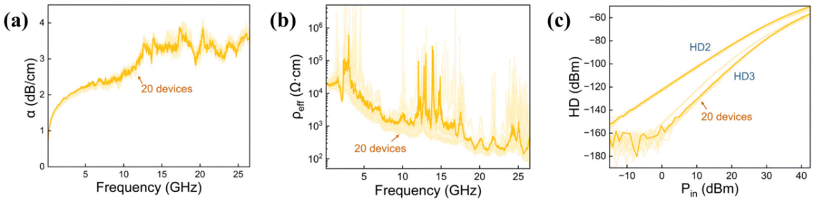 | ||
| Fig. 6 The (a) attenuation coefficient, (b) effective resistivity and (c) harmonic distortion of CPWs on the fabricated 300 mm RF-SOI. | ||
The 2nd and 3rd harmonic distortions (HD2 and HD3) were utilized to assess the linearity of the RF-SOI substrates. The analysis of the 20 CPW devices revealed a high degree of consistency in HD2. While some devices displayed a marginal reduction in HD3 at input powers below 20 dB m, their HD3 curves aligned with those of other devices at higher power levels. These results substantiated that the prepared 300 mm RF-SOI wafer met the stringent criteria for advanced radio-frequency substrates. Compared with other relative reports (Table 1), all of the RF performance not only demonstrated the feasibility and consistency of the fabrication process but also indicated the potential for high-yield device manufacturing on the same wafer, thereby reinforcing the robustness of fabrication of the 300 mm RF-SOI wafer.
4. Conclusion
In summary, this work successfully achieved the fabrication of 300 mm RF-SOI wafers with high-volume manufacturing potential, employing an optimized flow based on layer transfer and well-designed thermal treatment technology. Through the utilization of elaborate APCVD and in situ annealing, the compressive stress within the Poly-Si layer has been effectively mitigated to below 45 MPa. Combining the CMP process, a low-stress Poly-Si layer was prepared on the 300 mm HR-Si wafer, which exhibited excellent properties of wafer warpage below 60 μm. By employing oxidation thinning, the discrete surface of the as-split RF-SOI wafer could be transformed into a continuous surface, which was conducive to surface self-diffusion. The following non-contact smoothing effectively achieved a high degree of surface flatness at all tested frequency bands. Consequently, an integrated process combining oxidation thinning and non-contact smoothing technology has been proposed to effectively smooth the Top-Si layer to less than 3 Å. Moreover, the thickness uniformity of the Top-Si, BOX, and Poly-Si layers was controlled under 1%, 0.15%, and 6%, respectively. Upon small- and large-signal analyses, the α, ρeff and HD of RF-SOI were, respectively, 2.2 dB cm−1@5 GHz, 10 kΩ cm@5 GHz, and −95 dB m@900 MHz, satisfying the stringent requirements of advanced RF devices.Data availability
The data that support the findings of this study are available upon reasonable request from the authors.Conflicts of interest
The article follows all ethical standards and does not involve plagiarism, irregularities, etc.Acknowledgements
This work was financially supported by the National Key R&D Program of China (Grant No. 2022YFB4401700), National Natural Science Foundation of China (Grant No. 62074152 and 62304232) and Autonomous Deployment Project of China National Key Laboratory of Materials for Integrated Circuits (No. NKLJC-Z2023-A01).References
- H. Miao, J. Zhang, P. Tang, L. Tian, X. Zhao, B. Guo and G. Liu, IEEE J. Sel. Areas Commun., 2023, 41, 1945–1960 Search PubMed.
- M. Rack, F. Allibert and J.-P. Raskin, IEEE Trans. Electron Devices, 2021, 68, 4606–4613 CAS.
- L. Nyssens, M. Rack and J.-P. Raskin, in New Materials and Devices Enabling 5G Applications and Beyond, Elsevier, 2024, pp. 33–55 Search PubMed.
- I. Radu, A. Boussagol, A. Barthelemy and S. Vincent, ECS Trans., 2008, 16, 349–360 CrossRef CAS.
- T. E. Rudenko, A. N. Nazarov and V. S. Lysenko, Semicond. Phys., Quantum Electron. Optoelectron., 2020, 23, 227–252 CrossRef CAS.
- P. Sarafis, E. Hourdakis, A. G. Nassiopoulou, C. Roda Neve, K. Ben Ali and J.-P. Raskin, Solid-State Electron., 2013, 87, 27–33 CrossRef CAS.
- K. Ben Ali, C. Roda Neve, A. Gharsallah and J.-P. Raskin, in 2012 IEEE International SOI Conference (SOI), IEEE, NAPA, CA, 2012, pp. 1–2.
- Y. Wu, S. Gamble, B. M. Armstrong, V. F. Fusco and J. A. C. Stewart, IEEE Microw. Guid. Wave Lett., 1999, 9, 10–12 Search PubMed.
- D. Lederer and J.-P. Raskin, Solid-State Electron., 2005, 49, 491–496 CrossRef CAS.
- C. R. Neve, K. Ben Ali, C. Malaquin, F. Allibert, E. Desbonnets, I. Bertrand, W. Van Den Daele and J. Raskin, in 2013 IEEE 13th Topical Meeting on Silicon Monolithic Integrated Circuits in RF Systems, IEEE, Austin, TX, 2013, pp. 15–17.
- C. Roda Neve and J.-P. Raskin, IEEE Trans. Electron Devices, 2012, 59, 924–932 Search PubMed.
- D. C. Kerr, J. M. Gering, T. G. McKay, M. S. Carroll, C. R. Neve and J.-P. Raskin, in 2008 IEEE Topical Meeting on Silicon Monolithic Integrated Circuits in RF Systems, 2008, pp. 151–154.
- D. Lederer and J.-P. Raskin, IEEE Electron Device Lett., 2005, 26, 805–807 CAS.
- P. Mehr, X. Zhang, W. Lepkowski, C. Li and T. J. Thornton, Solid-State Electron., 2018, 142, 47–51 CrossRef CAS.
- L. Zhu, Y.-W. Chang, N. Gao, X. Su, Y. Dong, L. Fei, X. Wei and X. Wang, Chin. Phys. Lett., 2018, 35, 047302 CrossRef.
- A. Auberton-Herve, A. Wittkower and B. Aspar, Nucl. Instrum. Methods Phys. Res., Sect. B, 1995, 96, 420–424 CrossRef CAS.
- J. B. Lasky, S. R. Stiffler, F. R. White and J. R. Abernathey, in 1985 International Electron Devices Meeting, IRE, 1985, pp. 684–687.
- J.-P. Colinge, Silicon-on-Insulator Technology: Materials to VLSI, Springer US, Boston, MA, 1997 Search PubMed.
- T. Kim and J. Lee, Micro Nano Syst. Lett., 2023, 11, 15 CrossRef.
- A. C. Diebold and B. Doris, Surf. Interface Anal., 1993, 20, 127–139 CrossRef CAS.
- S. A. Ajuria and R. Reif, J. Appl. Phys., 1991, 69, 662–667 CrossRef CAS.
- Y. T. Chiang, Y. K. Fang, Y. J. Huang, T. H. Chou, S. Y. Yeh and C. S. Lin, Microelectron. Reliab., 2008, 48, 1786–1790 CrossRef CAS.
- T. A. Kato, Jpn. J. Appl. Phys., 1993, 32, 1879 CrossRef.
- N. Gao, M. Chen, H. Xu, Z. Xue, N. Zhang, L. Fei and X. Wei, Mater. Sci. Semicond. Process., 2020, 117, 105159 CrossRef CAS.
- P. E. Acosta-Alba, Influence of Smart CutTM process’ technological steps on the thickness uniformity of SOI wafers: Multi-Scale approach. Materials Science, Université Paul Sabatier- Toulouse III, 2014 Search PubMed.
- N. Gao, Y. Gao, M. Chen, H. Xu, Z. Xue and X. Wei, Mater. Sci. Semicond. Process., 2021, 130, 105842 CrossRef CAS.
- M. K. Weldon, V. E. Marsico, Y. J. Chabal, A. Agarwal, D. J. Eaglesham, J. Sapjeta, W. L. Brown, D. C. Jacobson, Y. Caudano, S. B. Christman and E. E. Chaban, J. Vac. Sci. Technol., B:Microelectron. Process. Phenom., 1997, 15, 1065–1073 CrossRef CAS.
- R. Dai, Y. Liu, Z. Wang, M. Li, T. Wei, Z. Xue and X. Wei, Semicond. Sci. Technol., 2023, 38, 095002 CrossRef CAS.
- K. T. Turner and S. M. Spearing, J. Appl. Phys., 2002, 92, 7658–7666 CrossRef CAS.
- W. Feng, H. Shimamoto, T. Kawagoe, I. Honma, M. Yamasaki, F. Okutsu, T. Masuda and K. Kikuchi, IEEE Trans. Electron Devices, 2022, 69, 6265–6269 Search PubMed.
- J. P. Colinge, E. Demoulin, F. Delannay, M. Lobet and J. M. Temerson, J. Electrochem. Soc., 1981, 128, 2009–2014 CrossRef CAS.
- X. Guo, M. Li, L. Li, P. Liu, C. Zhao and Z. Liu, in 2013 13th IEEE International Conference on Nanotechnology (IEEE-NANO 2013), IEEE, Beijing, China, 2013, pp. 950–953.
- R. Dai, Y. Liu, J. Ding, C. Shi, Z. Wang, Z. Xue and X. Wei, Mater. Sci. Semicond. Process., 2024, 177, 108330 CrossRef CAS.
- D.-S. Chao, Y.-C. Hsiao, J.-H. Liang and C.-M. Lin, Surf. Coat. Technol., 2020, 394, 125872 CrossRef CAS.
- L. Zhu, S. Liu, F. Allibert, E. Desbonnets, I. Radu, X. Zhu and Y. Lu, in 2016 International Symposium on VLSI Technology, Systems and Application (VLSI-TSA), IEEE, Hsinchu, 2016, pp. 1–2.
- S. Cheng, Y.-W. Chang, N. Gao, Y.-M. Dong, L. Fei, X. Wei and X. Wang, Chin. Phys. Lett., 2017, 34, 068101 CrossRef.
Footnote |
| † These authors contributed equally to this work and should be considered co-first authors. |
| This journal is © The Royal Society of Chemistry 2025 |