
 Open Access Article
 This Open Access Article is licensed under a Creative Commons Attribution-Non Commercial 3.0 Unported Licence
Mapping the local stoichiometry in Cu nanoparticles during controlled oxidation by STEM-EELS spectral imaging†
Eleonora
Spurio‡
 *ab,
Giovanni
Bertoni‡
*a,
Sergio
D'Addato
ab,
Francesca
Alimonti
c and
Paola
Luches
a
*ab,
Giovanni
Bertoni‡
*a,
Sergio
D'Addato
ab,
Francesca
Alimonti
c and
Paola
Luches
a
aCNR - Istituto Nanoscienze, Modena, Italy. E-mail: eleonoraspurio@unimore.it; giovanni.bertoni@cnr.it
bDipartimento FIM, Università degli Studi di Modena e Reggio Emilia, Modena, Italy
cDipartimento di Scienze Chimiche e Geologiche, Università degli Studi di Modena e Reggio Emilia, Modena, Italy
First published on 19th December 2024
Abstract
Copper nanoparticles (NPs) can be coupled with cuprous oxide, combining photoelectrocatalytic properties with a broad-range optical absorption. In the present study, we aimed to correlate changes in morphology, electronic structure and plasmonic properties of Cu NPs at different stages of oxidation. We demonstrated the ability to monitor the oxidation of NPs at the nanometric level using STEM-EELS spectral maps, which were analyzed with machine learning algorithms. The oxidation process was explored by exposing Cu NPs to air plasma, revealing systematic changes in their morphology and composition. Initial plasma exposure created a Cu2O shell, while prolonged exposure resulted in hollow structures with a CuO shell. This study identified procedures to obtain a material with Cu2O surface stoichiometry and absorption extended into the near-infrared range. Moreover, this study introduced a novel application of machine learning clustering techniques to analyze the morphological and chemical evolution of a nanostructured sample.
1. Introduction
Research in the field of photocatalytic materials for the direct conversion of solar energy into chemical energy has become extremely relevant and urgently needed. Plasmonic metal nanoparticles (NPs) possess unique optical properties that make them appealing candidates for photocatalytic applications.1–3 The optical properties of plasmonic NPs arise from their characteristic response, known as localized surface plasmon resonance (LSPR), which is the collective resonant excitation of charges. This phenomenon causes intense spectral absorption and scattering, as well as strong electromagnetic near-field enhancements at the resonant frequency.2,3 The LSPR energy position, along with the intensity and linewidth of the LSPR-related absorption band, primarily depends on the NP material. However, it has also been demonstrated that these properties are influenced by the size, shape and density of the NPs and their dielectric environment.4–7 The ability of plasmonic NPs to concentrate electromagnetic fields, scatter radiation, or convert electromagnetic energy into heat, coupled with the ability to tune their optical properties, makes them promising candidates in the field of photocatalysis.2 However, due to the extremely short lifetime of LSPRs, plasmonic NPs are often combined with semiconductors to which they can transfer charge and/or energy, thereby enhancing the rate of selected photochemical reactions. Metal NPs such as Cu, Au and Ag NPs are particularly attractive for photocatalytic applications because they support plasmon resonances that are tunable in the ultraviolet-visible-near infrared (UV–vis–NIR) region.2,8,9 Ag and Au are the most popular materials for plasmonic photocatalysis, but their high costs hinder potential large-scale applications.10,11 Cu offers a viable alternative to noble metal NPs, as it is an abundant and low-cost element that is also easy to prepare in the form of a nanomaterial.12 Due to its promising properties, nanocatalysts based on Cu can be applied in nanotechnology, electrocatalysis, and photocatalysis.12 The main limitation of Cu NPs is their stability, as they can be oxidized upon exposure to air or water.12 However, the use of Cu-based nanomaterials in electrocatalysis and photocatalysis has seen consistent advancements over the past few decades.8,10,12,13 Moreover, copper oxides also exhibit attractive photocatalytic properties, thanks to their bandgaps in the visible range (≃2.2 eV for Cu2O and ≃1.7 eV for CuO),14,15 as well as their abundance and non-toxicity.16 Furthermore, both CuO and Cu2O have a suitable bandgap for the hydrogen evolution reaction,15 and Cu2O also permits the oxygen evolution reaction,14 which is the rate limiting reaction in solar photoelectrocatalytic water splitting. The combination of plasmonic NPs with semiconductors has already been demonstrated to improve the performance of photocatalysts;17–19 and it has already been shown that the formation of heterostructures composed of Cu NPs and copper-based oxides is a promising pathway to obtain efficient materials for solar-light photocatalysis.20,21Interestingly, the controlled surface oxidation of Cu NPs can lead to the formation of a surface oxide shell that may simultaneously extend the photon absorption range, enhance the photocatalytic properties, and protect the metal core from further oxidation.22–24 The importance of Cu-based nanostructures and core@shell NPs is demonstrated by the vast literature on their growth, including both chemical and physical synthesis techniques. Over the decades, numerous investigations have been conducted to grow NPs with varying dimensions in diverse environments, and to characterize and tune the dependence of their optical response and morphology on these factors and on the NPs oxidation.25–29
Transmission electron microscopy (TEM) is a suitable technique to understand the oxidation processes at the nanoscale.30 Scanning transmission electron microscopy (STEM) coupled with electron energy-loss spectroscopy (EELS) is able to clearly reveal the local oxidation state in transition metal NPs.31–33 The valence state of Cu can be determined in the core and shell regions of NPs, by quantifying the Cu and O concentration from their spectra, and by inspecting the spectral features in the ionization edge fine structures (energy-loss near-edge structure, or ELNES). Metallic Cu is characterized by a two step-like onset in its L23 ionization edge, while Cu(1) and Cu(2) are indicated by the presence of peaks with increasing intensities at the onset (the so-called white-lines, in analogy with X-ray absorption) due to the Cu d-bands being progressively emptied by electronic transfer to oxygen atoms in the oxides.34,35 The advantage of STEM-EELS is the possibility to investigate these features with a spatial resolution below the nanometer scale, and to provide oxidation maps on individual NPs. Moreover, the crystal ordering requirements of the phases as in electron diffraction are not required.36 In recent years, these kind of spectral mapping analyses have become more common, due to the added technical advancements in signal de-noising and spectral decomposition from machine learning (ML) algorithms,37,38 which nowadays can be run even on standard PCs. Even though the oxidation behavior of copper has been largely studied in the literature,4,39–43 systematic correlation of the morphological, electronic, and optical properties at the different oxidation stages has, to the best of our knowledge, not been investigated in detail yet.
In this work, we present a study of the evolution of a film of Cu NPs induced by exposure to air plasma. In particular, we link the observed changes of the morphology and local stoichiometry with the modification of the optical and plasmonic properties. Furthermore, we also demonstrate the possibility to reduce the oxidized NPs, exploring the reversibility of the oxidation process. This work presents an innovative application of machine learning data clustering to assess the morphological and chemical evolution of a nanostructured sample. The approach makes use of principal component analysis (PCA) to extract the statistically most significant components from the 3D spectra, with ML clustering performed in the featured space of the PCA components.44 This permits visualizing and comparing the results of different ML methods with the synthetic data, and selecting the most efficient to use for interpretation of the experimental data.
2. Experimental
The samples investigated in the present work were grown in an ultrahigh vacuum (UHV) apparatus (P ≃ 10−10 mbar), which included two connected UHV chambers:45 a preparation chamber, equipped with evaporators and gas lines for reactive molecular beam epitaxy (MBE) growth and a quartz microbalance to measure the evaporation rate, and a second chamber in which X-ray photoemission spectroscopy (XPS) and Auger emission spectroscopy (AES) analyses were performed. Cu was evaporated from a Knudsen cell on the substrate kept at room temperature (RT), and the Cu atoms self-assembled on the substrate forming Cu NPs.46 The nominal thickness of each sample was 2 nm, where the nominal amount refers to the equivalent thickness of a uniform Cu layer fully covering the substrate. The samples were grown either on UV-grade fused silica substrates for the optical absorbance measurements or on SixNy TEM membranes of 15 nm thickness for the TEM measurements. The SixNy thin substrates were chosen for TEM, STEM, and EELS measurements because of their high thermal stability, unlike common metallic TEM grids such as Ni, Cu, or Mo, in which metallic diffusion is typically found with the formation of large metallic or alloy particles after UHV annealing at high temperature.47,48 The quartz substrates were cleaned by a 5 min bath in acetone at 423 K and by two subsequent ultrasonic baths in acetone and in isopropanol at 353 K for 3 min each, while the TEM grids were cleaned for 4 min to remove carbon contamination in a SmartPlasma system operated at 32 W (at the kHz frequency) using air as the gas mixture and 0.1 mbar pressure. After the deposition, the Cu NPs were annealed at 773 K at an oxygen partial pressure PO2 of 10−7 mbar. After the deposition, the Cu NPs were exposed to the same air plasma for different times, namely 30, 90, and 120 s, while keeping the sample at RT during the processes. The use of reactive plasma – thanks to the high concentration of atomic oxygen49 – allowed enhancing the rate of oxidation of some materials.50–52 After the plasma treatment, each sample was annealed for 30 min in UHV at 773 K. After each step (growth, plasma treatment, UHV annealing), each sample was investigated by AES using Al Kα photons from a double-anode X-ray source. Three reference samples of Cu(0), Cu(1), and Cu(2) were also prepared for comparison. The reference films were thicker than the samples investigated in the present work (6 nm each), and were grown and post-treated as described by the following:• Cu(0): UHV deposition at RT, post-annealing in UHV at 773 K for 30 min.
• Cu(1): Deposition at RT and PO2 = 3 × 10⁻⁶ mbar in three steps of 30 min each, annealing the film after each step for 20 min at 573 K. After the deposition, the film was annealed in air in a quartz tube furnace at 423 K in a mixture of 50% N2 and 50% O2 flux for 30 min. Afterwards, the film was annealed in UHV for 30 min at 573 K.
• Cu(2): Deposition at RT and PO2 = 3 × 10⁻⁶ mbar in three steps as described for Cu(1). The film was then annealed in the quartz tube furnace at 623 K in a mixture of 50% N2 and 50% O2 for 120 min.
In order to investigate the chemical composition of the samples, the Cu L23M45M45 emission lines were acquired, using a hemispherical electron analyzer with a pass energy of 30 eV at normal emission. In order to extract the chemical composition of each sample, the Cu L23M45M45 emission lines after each step were fitted using the reference spectra in Fig. 1a, obtained from the reference samples described above. The first one shows a dominant peak at 918.6 eV, while the peak position was at 916.8 eV for Cu2O and at 917.7 eV for CuO, which were consistent with the values reported in the literature.53
 | ||
| Fig. 1 (a) Cu L23M45M45 spectra of Cu(0), Cu(1), and Cu(2), acquired from reference samples. For a better comparison, the area under each curve is normalized to 1, and the spectra are shifted equidistantly along the vertical axis; (b) extracted near-edge structures (ELNES) of the Cu L23 edge. | ||
The optical absorptance of the samples after each step was obtained by ultraviolet–visible (UV–Vis) spectrophotometry. The setup was composed of a xenon lamp, which provided white non-polarized light, an ORIEL-MS257 monochromator, a polarizer, and a silicon photodetector. The sample was mounted with the surface normal forming a 22° angle with the impinging photon beam. The absorptance (A) of the sample was evaluated as A = 1 − (T + R), where T and R are the transmittance and the reflectance, i.e., the fraction of transmitted and reflected light, acquired with s-polarized radiation.
To compare the experimental results with the theoretical expectations, we simulated the optical responses of the NPs by using the MNPBEM toolbox, developed by Hohenester and coworkers54 based on the boundary element method (BEM) approach.55 The extinction coefficient of the NPs was calculated assuming the NPs to be metallic and surrounded by a medium characterized by an optical index of 1.575, in between those of quartz (substrate) and air (superstrate), as suggested in ref. 43. The bulk dielectric functions used in the simulations were taken from ref. 56 for Cu and from ref. 57 for Cu2O, while the dielectric function of quartz was calculated from the Sellmeier equation58 using the coefficient of fused SiO2 at RT.59 In the simulations, the NPs were approximated as ellipsoids, while the light was assumed to be linearly polarized and at normal incidence. Possible interactions between the NPs were neglected.
The morphological modifications induced by the plasma treatment were systematically investigated using transmission electron microscopy (TEM) imaging, scanning transmission electron microscopy in the dark field mode (ADF-STEM), and electron energy-loss spectroscopy (EELS) with a ThermoFisher Talos FS200 equipped with a Schottky gun at 200 kV and a Gatan Enfinium EELS spectrometer. EELS was performed in the STEM mode, with an analytical probe of ∼0.5 nm. The spectral images (SI) were acquired from representative NPs after every step under the very same acquisition conditions, meaning the same spot size, same convergence aperture (semi-angle 10.5 mrad), and same collection angle of the EELS spectrometer (semi-angle 17.4 mrad) for reliable comparison of the results. The spectra were acquired with 0.5 eV dispersion, allowing simultaneous acquisition of the O K edge at ∼532 eV and the Cu L23 edge at ∼931 eV. Core–shell maps of the NPs were obtained from clustering algorithms from machine learning (ML clustering), and implemented with Python custom scripts and the library sklearn. To assign the Cu oxidation state, the extracted spectra after classification were compared with the near-edge structure (ELNES) of the Cu-L23 edge acquired on the three reference samples, shown in Fig. 1b.
Simulated data machine learning clustering
Before analyzing the experimental samples using EELS mapping, we tested the effectiveness of machine learning clustering algorithms with the synthetic data. In this way, the expected results (the labels of the classes) are known (ground true), and the various methods of ML clustering can be compared. These can be classified as unsupervised if the labeling of the data is unknown. This is the typical case in experiments in which we do not know which points in the particles have to be assigned to one of the 3 classes (core, shell, or the substrate). The most well-known unsupervised methods are K-means (KM), Gaussian mixture model (GMM), and agglomerative clustering (AGC). KM is the workhorse of the clustering methods, and simply relies on iteratively assigning a point to the one of the expected classes from which the point has the lowest distance (with respect to the mean center of the class). GMM assumes that the probability distributions of the points in the classes are normally distributed (i.e., Gaussian). AGC starts by assuming that each point represents a separate class, and hierarchically merges the points in pairs until a threshold (or the expected number of classes, 3 in our case) is reached. Supervised methods, instead, rely on prior knowledge of the labeling for a subset of the data, from which a model can be learned and applied to the whole dataset, with expected better results. Unfortunately, this is rarely the case in experiments, unless part of the same data was analyzed with a different (and much trusted) technique. The most notable of the supervised methods is support vector machine (SVM), which aims to find hyperplanes separating the classes in the data and can be considered as a pioneer of deep learning methods, making use of dimensional augmentation and kernels. For a better understanding of the different algorithms, we refer the reader to the book by Brunton and Kutz.44 The test synthetic data were built considering a NP with a Cu core of 10 nm and a CuO shell of 1.5 nm, on top of a 10 nm substrate made of amorphous carbon of approx. 10 nm thickness.We considered carbon for simplicity, with its K edge at 284 eV, before the O and Cu edges, not far from the K edge of N at 400 eV found in SixNy. We generated the 3D EELS dataset considering a convergence angle of 10.5 mrad, a collection angle of 17.4 mrad, a current in the beam of 40 pA, and noise corresponding to a DQE of 0.5 from the CCD detector. An example of such a 3D EELS dataset is shown in Fig. 2. Fig. 2(a) shows the dataset integrated in the energy coordinate, while Fig. 2(b) reports the average EEL spectrum and the spectrum from the central point in the particle. Fig. 2(c) compares the resulting labelling from the different unsupervised methods, calculated as the root mean squared error (RMSE) with respect to the ground truth (or true labels). All the ML clustering processes were run in the space of the first 10 PCA components, to be sure to account for >95% of the variance in the data, instead of using the full 2048 points in the EEL spectra, resulting in a very fast computation (few seconds on a desktop PC). Fig. 2(d) presents the simulated dataset in the 2D featured space of the first two PCA components (it is not possible to easily show the 10 dimensional space used in the clustering process). By comparing the errors with respect to the true labels (RMSE), the AGC was found to be the most precise with the synthetic data (0.03, or 99% accuracy), followed by KM (0.22, 96%), and finally GMM (0.35, 93%), which seemed to suffer from noisy data, resulting in a slightly thicker shell. For comparison, the state-of-art SVM gave an RMSE close to zero, meaning that almost all the points were correctly classified (100% accuracy). Overall, all the unsupervised methods correctly identified the three classes with an accuracy >90%. This is promising for the analysis of experimental data with a similar signal to noise ratio (about 8.2 dB from the average spectrum and E > 500 eV).
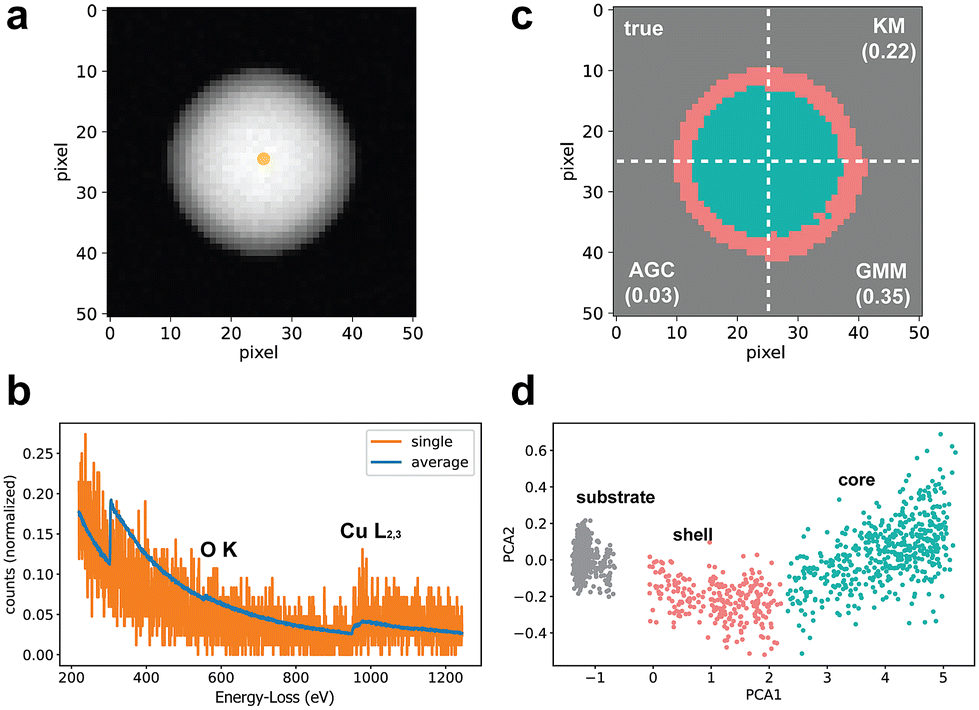 | ||
| Fig. 2 Results of ML clustering with the synthetic data from a core–shell Cu/CuO NP. (a) Simulated EELS dataset (2D view after integration in the energy channels). 1 pixel is 0.5 nm. (b) Comparison between the average spectrum from the whole dataset and the spectrum taken from the center of the NP. The O K and Cu L edges are indicated. The edge at ∼300 eV is from the (carbon) substrate. (c) Comparison of the resulting labelling from K-means (KM), Gaussian mixture models (GMM), and agglomerative lustering (AGC). The RMSE values are reported within the parentheses. For comparison, the supervised SVM has an RMSE of 0.01. (d) Featured 2D space of the first two PCA components. The points are colored according to the expected true labels. | ||
3. Results and discussion
Comparison of the as-grown and annealed samples
Before the plasma treatments, the Cu NPs were annealed for 30 min at 773 K in an oxygen partial pressure PO2 of 10−7 mbar. To understand the effects of this treatment on the NPs, they were studied in terms of their morphology via TEM imaging, chemical composition via AES, and optical properties via UV–Vis spectrophotometry. The results were compared with the properties of NPs measured directly after their growth.The TEM images of the sample before and after the annealing are shown in Fig. 3a and c, respectively. Fig. 3b and d show the diameter distribution of the as-grown and the post-annealed samples, fitted using a log–normal distribution (red curve in the images). The as-grown NPs had an average diameter of 9 ± 3 nm, while the post-annealed NPs were characterized by a higher average diameter of 13 ± 4 nm, a slightly higher density and a more regular shape. The coverage was around 49% in Fig. 3b and 42% in Fig. 3a. The average height of the NPs was estimated by dividing the nominal thickness of the Cu layer (2 nm) by the coverage extracted from the TEM images, obtaining h = 4.1 nm for the as-grown and h = 4.8 nm for the post-annealed NPs.
 | ||
| Fig. 3 (a) and (c) TEM images and (b) and (d) diameter distributions of as-grown and post-annealed Cu NPs, respectively. | ||
Fig. 4a presents the AE spectra, which were more sensitive to the oxidation state of Cu compared to XPS,53,60 before and after the annealing. The two curves were very similar to each other, with a main peak at 918.6 eV typical of metallic copper.53 The concentration of copper oxides was negligible in both cases, compatible with the oxygen partial pressure that was too low to oxidize the NPs.60
 | ||
| Fig. 4 (a) AES Cu L23M45M45 spectra of the as-grown (yellow) and post-annealed (blue) samples (b) experimental optical absorptance of the NPs directly after growth and after annealing. (c) Simulated extinction cross-sections obtained by using the diameter distribution shown in Fig. 3b and d for the as-grown and post-annealed NPs. (d) Simulated extinction cross-section considering one single spheroidal NP (yellow curve) and two interacting NPs (green dashed curve), with diameters equal to the average diameter of the as-grown NPs. | ||
Fig. 4b shows the optical absorptance spectra of the as-grown and the post-annealed samples in yellow and in blue, respectively. In both cases, the optical absorptance showed a dominant absorbance band in the visible range, ascribed to the excitation of the LSPR in the Cu NPs.42 The difference in broadness and in peak position of the two curves was ascribed to the different morphologies of the two samples. In particular, the as-grown NPs were smaller, denser (i.e., closer to each other), and characterized by an irregular shape. The effect of the annealing was to enlarge and separate the NPs, which also became more regularly shaped. Fig. 4c shows the numerical simulations obtained with the MNPBEM toolbox,54 using the diameter distributions shown in Fig. 3b and d. Coherently with the experimental curves in Fig. 4b, the extinction cross-section was narrower and blue-shifted when simulated with the distribution characteristic of the post-annealed NPs. The differences between the simulated extinction cross-section and the measured optical absorbance could be ascribed to the approximations made in the model, especially to the fact that the interparticle interactions were neglected. This represents a strong assumption, being that the NPs were relatively large and very close to each other, and the main role of the simulation shown in Fig. 4c was to justify the differences between the annealed and the as-grown NPs, and not to accurately reproduce the experimental results. Indeed, as shown in Fig. 4d, the simulated extinction cross-sections of a single isolated NP and two interacting NPs differed both in shape and peak position. The simulations were performed assuming the NPs to be ellipsoidal, with a diameter equal to the average one of the as-grown NPs (9 nm). The yellow curve shows the extinction cross-section of a single, isolated NP while the green dashed curve is the simulated extinction cross-section for two interacting NPs separated by 2 nm. The main effects of this interaction was an increase in the extinction cross-section and a red-shift of the absorptance peak.
Effects of plasma oxidation
To induce a controlled progressive oxidation of the surface of the NPs, we exposed the sample to plasma for increasing times and followed the modifications in the morphology and local stoichiometry by STEM imaging combined with EELS. For each exposure time, Fig. 5 reports in the left panel the STEM image, while the inset shows the results obtained by AGC clustering on a SI map of an individual NP, and the right panel shows the average EEL spectrum for each component identified. Before any plasma treatment, after the annealing in UHV-compatible oxygen pressures (Fig. 5a), the image could be described using only two components. The first one corresponded to metallic Cu (blue) and it represented the NPs, while the second one was ascribed to the substrate (gray). The same result was obtained by increasing the number of components in the clustering. After 30 s of plasma treatment (Fig. 5b), three components were needed to describe the SI. Two of them arose from different regions in NPs: a core with a metallic Cu character (blue), with a diameter of ≃15.5 nm, and a shell, of ≃3 nm thickness, containing primarily Cu2O (violet). The third component (gray) was again due to the contribution from the substrate. The assignment was based on the shape of the EEEL spectrum (right panel): in the Cu L edge, the white-lines intensity increased in the shell region, as expected in Cu2O, while the O K signal was hardly visible, due to the high background signal from the substrate. However, the quantification by using the Hartree–Slater cross-sections matched well with the Cu2O composition in the shell. Also, in the core region, the intensity of the O K edge-related signal was very low but non-negligible, possibly due to the presence of the shell on the top and bottom of the NPs. The oxides formed shells with a rather irregular shape, which in some cases extended over the substrate connecting two or more NPs. After 90 s of plasma treatment (Fig. 5c), two components were needed to describe the NPs, in addition to the contribution from the substrate. The lateral size of the Cu(0) cores decreased by ≃60%, while the thickness of the surrounding Cu2O increased, and the morphology of the sample changed: the NPs appeared to be partially agglomerated, and some of them were starting to show the formation of internal voids, ascribed to the nanoscale Kirkendall effect61 (see the white arrows in the STEM image in Fig. 5c). This effect has been observed in some metallic nanostructures, and it has been reported to be due to an unbalanced diffusion of O and Cu ions in the oxide, causing the conversion of the metallic NP into a hollow oxide shell.41,42,62 Some oxygen was visible in the core region, due to the thicker shell (star in the right panel of Fig. 5c). After 120 s of plasma exposure (Fig. 5d), the majority of the NPs were completely oxidized, and their composition was a mixture of CuO and Cu2O, as could be noticed by the significantly higher white line intensity in the EEL spectrum in the right panel. In the STEM image, the formation of internal voids due to the nano-Kirkendall effect was evident for the majority of the NPs. The hollow structures had a higher overall dimension than the initial NPs in Fig. 5a (≃20 nm in Fig. 5d and ≃13 nm in Fig. 5a), compatible with the presence of internal voids with an average diameter of ≃6 nm. From these observations, it could be noted that the average diameter of the internal voids was smaller with respect to the initial diameter of the NPs.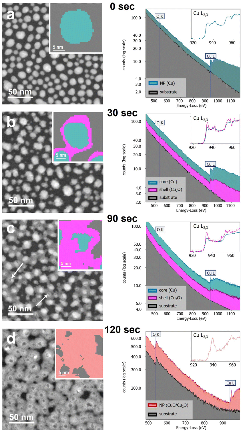 | ||
| Fig. 5 ADF-STEM images (left) and corresponding EEL spectra (right) of the Cu NPs. The left insets show the results after data clustering (AGC) from a single NP, and the right insets show the corresponding Cu L2,3 ELNES. (a) Before any plasma treatment: only a metallic Cu component (blue) and the substrate contribution (gray) were detected. (b) After 30 s of plasma exposure, a metallic core Cu(0) (blue), an oxide Cu(1) shell (violet), and the substrate (gray) were detected. (c) After 90 s of plasma exposure, a metallic core Cu(0) (blue), a thicker oxide Cu(1) shell (violet), and the substrate (gray) were detected. (d) After 120 s of plasma exposure, only 2 components were detected: fully oxidized Cu(1)/Cu(2) NP (pink), and the substrate (gray). | ||
If only Cu transport through the oxide layer were to be considered, the diameter of the vacancy would be expected to be the same as the initial diameter of the NP. However, according to ref. 39 and 63, both the inward diffusion of oxygen ions and the inward relaxation of the outer oxide shell must be taken into account, contributing to such a difference. Comparing the TEM images in Fig. 5a–d, it could be noted that with increasing the exposure time to air plasma, the hole size increased and the outward growth of the shell proceeded, consistent with what was observed and reported in ref. 63.
The results of the AGC clustering on the NPs were compared with the chemical composition of the sample surface obtained by the AES data, shown in Fig. 6a. Due to the surface sensitivity of the techniques, the spectra were only sensitive to the chemical composition of the outer shells after the different plasma treatments. In particular, the AES spectra, sensitive to the chemical state of the samples,53 were fitted using the spectra acquired on reference samples of Cu(0), Cu(1), and Cu(2), shown in Fig. 1a. The results of the fitting procedure are shown as solid lines in Fig. 6a and summarized in Table 1. The black triangles correspond to the Auger spectrum acquired for the sample post-annealed at UHV-compatible oxygen pressure, before any plasma treatment and the corresponding fitting (solid line). The spectrum shows the typical shape of Cu(0), with the main peak at 918.6 eV. The concentration of Cu(1) increased to ≃80%, after 30 s of plasma exposure (red triangles), while a small fraction of Cu(0) was still present on the sample surface, and no Cu(2) was formed yet. After 90 s of plasma exposure (yellow triangles), no more Cu(0) was detected with AES, compatible with the thicker oxide shell formed (Fig. 5c), while a small fraction of the sample surface had started to be oxidized to Cu(2). Finally, after 120 s (blue triangles), the AES spectrum could be fitted by a mixture of Cu(2) and Cu(1). These results are in good agreement with the components individuated via the AGC clustering presented in Fig. 5.
 | ||
| Fig. 6 (a) Cu L23M45M45 spectra of the sample after different plasma exposure times (triangles) and the results of the fitting procedure (solid lines). (b) Optical absorptance of the Cu NPs after different time exposures to plasma. (c) Simulated extinction cross-section of the metallic Cu NPs with a diameter distribution extracted from Fig. 5a and for Cu@Cu2O NPs, with a diameter distribution extracted from Fig. 5b and considering an average shell thickness of 2 nm. | ||
| Duration of plasma exposure (s) | Cu(0) (%) | Cu(1) (%) | Cu(2) (%) |
|---|---|---|---|
| 0 s | 100 | 0 | 0 |
| 30 s | 14 | 85 | 1 |
| 90 s | 2 | 82 | 16 |
| 120 s | 0 | 53 | 47 |
Fig. 6b reports the UV–Vis optical absorptance spectra of the sample after the first annealing in oxygen and after each plasma treatment. Many previous works have used optical absorptance as a signature of the metallic nature of Cu NPs,25–27 showing that the lower the Cu(0) concentration, the less intense was the LSPR-related absorptance peak. Moreover, for metallic Cu cores below certain dimensions, the LSPR-related absorptance could not be observed.25,26 As already mentioned, the optical absorptance of the sample before any exposure to plasma was compatible with the absorptance spectrum of metallic Cu NPs, with the absorptance band peak at 680 nm compatible with LSPR excitation. When the sample was exposed to plasma for 30 s, the LSPR peak broadened, with a decrease in intensity and shift toward slightly higher wavelength (maximum at 715 nm). This behavior was consistent with the formation of a thin cuprous oxide shell around the metallic NP,64 as also confirmed by the numerical simulations shown in Fig. 6c. The optical absorptance of the sample after 90 s of plasma exposure is shown as the yellow line in Fig. 6b, where it could be seen that the absorptance band related to LSPR in the metallic NPs was much less intense than in the previous samples, and only a weak absorptance band could be identified around 700 nm. The peak at ≃340 nm was ascribed to interband transitions in the oxide.65 The optical absorptance was consistent with the fact that after 90 s of exposure to plasma, only a small concentration of Cu(0) species was detected in the EELS spectrum (Fig. 5c). Finally, after 2 min of exposure to plasma, when the NPs had completely changed their shape and all of them were completely oxidized, the LSPR-related absorptance was zero and only the peak ascribed to interband transitions in the oxide were observed, with a peak around 350 nm.
Effects of UHV annealing
After 90 s of exposure to air plasma, the sample was annealed for 30 min in UHV conditions at 773 K. Fig. 7a shows a large-scale STEM image of the sample after the UHV annealing. A low density of large Cu NPs (white dots in the image) could be identified on the sample surface. The highlighted boxes in Fig. 7a of different regions of the sample are shown as zoomed-in images in Fig. 7b and c. The STEM-EELS analysis revealed a large metallic Cu core and a thin Cu2O shell surrounding the NP. The copper core of the NP had a diameter of ≃150 nm and an irregular shape, while accurate estimation of the thickness of the surrounding shell was limited by the pixel size used to acquire the map, ≃5 nm, which only gave an upper limit of the shell size. Due to the large size of the core (producing a diffraction contrast by being crystalline), the clustering algorithms could not extract both the core and shell regions when only a few classes were considered. Indeed, several classes result from the different orientations of the domains in the core. For this reason, in this case, principal component analysis (PCA) was used, and the different components forming the core were summed after inspection (same spectral features but different amplitudes, due to the different orientations of the domains). The result of the PCA analysis on a portion of the film is shown in the inset in Fig. 7b. The composition of the film on which the large NPs formed is shown in Fig. 7c, which appears very similar to that shown in Fig. 5c, suggesting that the majority of the sample did not show a changed morphology. From the results of the PCA analysis, it is possible to conclude that also the composition was very close: the film was mainly composed by Cu2O (in violet), with small metallic cores (blue). The formation of such large core–shell NPs could be ascribed to the annealing under reducing UHV conditions. The Cu atoms diffused through the oxide shell faster than O atoms, resulting in a net outward flow of Cu ions that diffused on the sample surface and agglomerated, forming relatively large metallic NPs.66 After the UHV annealing, the NPs were again exposed to plasma treatment for 2 min. The effects of these treatments on the morphology and on the composition of the NPs are shown in Fig. 7d. Even though the duration of the exposure to plasma was the same as for the sample shown in Fig. 5d, the final result was significantly different. In this case, the core of the NP remained metallic, and the effect of the plasma treatment on the large NPs was to thicken the Cu2O shell around the metallic core to ≃10 nm. | ||
| Fig. 7 (a) Large STEM image of the sample after 90 s of plasma treatment + 30 min of UHV annealing at 773 K; (b) STEM image of the region highlighted in yellow in panel a containing a large NP with a metallic core. Inset: result of the PCA analysis on the NP: a shell of Cu2O shell (violet) surrounds the metallic cores (blue), lying on a substrate mainly formed by Cu2O NPs (violet) with small metallic cores (blue); (c) enlargement of the region surrounded by the blue box in (a); (d) STEM image of an NP after 90 s of plasma treatment + 30 min of UHV annealing at 773 K + 120 s of plasma treatment, inset: result of the PCA analysis on the NP: the Cu2O shell (violet) became thicker, the core (blue) remained metallic, and the underlying film (pink) was composed of a mixture of Cu2O and CuO. | ||
On the other hand, the small NPs were predominantly oxidized to a mixture of CuO and Cu2O (Fig. 7d, inset), similar to Fig. 5d. This strong difference in behavior under plasma treatment was ascribed to the different sizes of NPs after UHV annealing. Indeed, as previously observed,41,43 the initial NP size is a critical parameter for the evolution of metal and oxide molar volumes, and for the time required for the oxidation of NPs.
The optical absorptance and AES spectra were acquired after the UHV annealing and after the subsequent 120 s of plasma treatment and are shown in Fig. 8. The LSPR-related absorption partially recovered after the annealing, with a peak appearing at ≃670 nm. The peak was decreased in intensity and red-shifted after the exposure to plasma, consistent with the thickening of the oxide shell around the particle. The low intensity of the plasmonic resonance compared to the intensity of the interband transition-related absorptance could be justified by the low concentration of the NPs after the UHV annealing (Fig. 7a). The fitting of the AES spectra, shown in Fig. 8b, confirmed the observations derived from the PCA analysis shown in the insets of Fig. 7b and d. After the UHV annealing (cyan triangles), the sample surface was composed of 80% Cu(1) and 20% Cu(2), while after the subsequent 120 s of plasma exposure (orange triangles), the sample presented a dominant Cu(2) component (65%).
 | ||
| Fig. 8 (a) Optical absorptance spectra of the sample after 90 s of plasma exposure (black line), after UHV annealing (blue line), and after a second exposure of 120 s to plasma (orange line); (b) Cu L23M4,5M4,5 spectra of the sample after UHV annealing (cyan triangles) and 120 s of subsequent plasma annealing (orange triangles) fitted with the reference spectra in Fig. 1. | ||
The UHV annealing procedure was repeated also for the sample exposed to 120 s of plasma exposure. However, in this case, the complete absence of Cu(0) left in the sample prevented the formation of large and dispersed Cu NPs and the plasmonic resonance was not recovered (Fig. S1†).
4. Conclusions
The present work shows that it is possible to follow the oxidation of Cu NPs in nanometric detail by STEM-EELS spectral maps analyzed using machine learning-based algorithms, here using the oxidation of Cu NPs as a case study. The results obtained by STEM-EELS were shown to be compatible with the space averaged results from electron spectroscopy techniques and with the optical response of the system. In particular, we systematically investigated the morphology and composition evolution of thin Cu NPs films as a function of exposure to air plasma, correlating the observed modifications with the observed changes in plasmonic properties. After the growth and a first annealing in oxygen under UHV-compatible conditions, the NPs were found to be completely metallic and had a regular shape. A short exposure to air plasma (30 s) induced the formation of a thin Cu2O shell surrounding the NPs, while the dimensions of the NPs and the substrate coverage remained essentially unmodified. When the NPs were exposed to plasma for longer times (90 s), the NPs change both their composition and morphology; whereby the metallic core shrank, while the oxide shell was thickened. Also, some of the NPs started to exhibit the internal voids typical of the nano-Kirkendall effect, surrounded by a Cu2O shell. The morphology also changed; whereby the oxide expanded over the substrate and partially interconnected the NPs. Finally, after 120 s of plasma treatment, the majority of NPs presented a hollow structure, with a CuO shell. The STEM-EELS maps, in good agreement with the surface chemical composition, measured by electron spectroscopy, could explain the optical absorptance spectra measured at the different steps. After 30 s of plasma treatment, the LSPR was red-shifted, compatible with the results of the numerical simulations for a system composed by core@shell Cu@Cu2O NPs. After 90 s, only a weak plasmonic band was present, and this completely disappeared when the NPs were treated for 120 s with plasma, consistent with the observed progressive decrease in size of the metallic core.When the sample treated for 90 s in plasma was annealed in UHV, the Cu(0) ions tended to diffuse and agglomerate, forming large Cu NPs (diameter ≃150 nm) surrounded by a thin Cu2O shell of ≃5 nm. When these large nanostructures were exposed to plasma treatment for 120 s, the metallic Cu core remained almost unchanged, and the only effect of the treatment was to slightly increase the thickness of the Cu2O shell around the NPs.
Data availability
All the data that support the findings of this study are included within the article (and any ESI†).The data supporting this article are available at https://github.com/gbertoni/Data-for-NR-ART-10-2024-004341.git.
Conflicts of interest
There are no conflicts to declare.Acknowledgements
This work was supported by the PNRR MUR project ECS-00000033-ECOSISTER and by the European Union-NextGenerationEU Mission 4 Component 2 (National Sustainable Mobility Center CN00000023, Italian Ministry of University and Research Decree no. 1033, 17/06/2022, Spoke 11, Innovative Materials & Lightweighting and Infrastructure for Energy Transition and Circular Economy – iENTRANCE@ENL IR0000027, and PRIN 2022 PNRR ResET CUP: B53D23028720001).References
- A. Gellé and A. Moores, Curr. Opin. Green Sustain. Chem., 2019, 15, 60–66 CrossRef.
- S. Linic, P. Christopher and D. B. Ingram, Nat. Mater., 2011, 10, 911–921 CrossRef CAS PubMed.
- P. Christopher, H. Xin and S. Linic, Nat. Chem., 2011, 3, 467–472 CrossRef CAS PubMed.
- G. H. Chan, J. Zhao, E. M. Hicks, G. C. Schatz and R. P. Van Duyne, Nano Lett., 2007, 7, 1947–1952 CrossRef CAS.
- C. L. Haynes and R. P. Van Duyne, J. Phys. Chem. B, 2001, 105, 5599–5611 CrossRef CAS.
- L. J. Sherry, R. Jin, C. A. Mirkin, G. C. Schatz and R. P. Van Duyne, Nano Lett., 2006, 6, 2060–2065 CrossRef CAS PubMed.
- F. Parveen, B. Sannakki, M. V. Mandke and H. M. Pathan, Sol. Energy Mater. Sol. Cells, 2016, 144, 371–382 CrossRef CAS.
- S. Kim, J. Kim, J. Park and J. Nam, Adv. Mater., 2018, 30, 1704528 CrossRef PubMed.
- U. Aslam, V. G. Rao, S. Chavez and S. Linic, Nat. Catal., 2018, 1, 656–665 CrossRef.
- Y. Xin, K. Yu, L. Zhang, Y. Yang, H. Yuan, H. Li, L. Wang and J. Zeng, Adv. Mater., 2021, 33, 2008145 CrossRef CAS PubMed.
- X. Wang, C. Zhang, X. Zhou, Z. Fu, L. Yan, J. Li, Z. Zhang and H. Zheng, Nanomaterials, 2022, 12, 2927 CrossRef CAS PubMed.
- M. B. Gawande, A. Goswami, F.-X. Felpin, T. Asefa, X. Huang, R. Silva, X. Zou, R. Zboril and R. S. Varma, Chem. Rev., 2016, 116, 3722–3811 CrossRef CAS PubMed.
- D. Wang and D. Astruc, Chem. Soc. Rev., 2017, 46, 816–854 RSC.
- S. J. A. Moniz, S. A. Shevlin, D. J. Martin, Z.-X. Guo and J. Tang, Energy Environ. Sci., 2015, 8, 731–759 RSC.
- R. Siavash Moakhar, S. M. Hosseini-Hosseinabad, S. Masudy-Panah, A. Seza, M. Jalali, H. Fallah-Arani, F. Dabir, S. Gholipour, Y. Abdi, M. Bagheri-Hariri, N. Riahi-Noori, Y. Lim, A. Hagfeldt and M. Saliba, Adv. Mater., 2021, 33, 2007285 CrossRef CAS PubMed.
- T. Baran, A. Visibile, M. Busch, X. He, S. Wojtyla, S. Rondinini, A. Minguzzi and A. Vertova, Molecules, 2021, 26, 7271 CrossRef CAS PubMed.
- J. S. Pelli Cresi, E. Principi, E. Spurio, D. Catone, P. O'Keeffe, S. Turchini, S. Benedetti, A. Vikatakavi, S. D'Addato, R. Mincigrucci, L. Foglia, G. Kurdi, I. P. Nikolov, G. De Ninno, C. Masciovecchio, S. Nannarone, J. Kopula Kesavan, F. Boscherini and P. Luches, Nano Lett., 2021, 21, 1729–1734 CrossRef CAS PubMed.
- N. Wu, Nanoscale, 2018, 10, 2679–2696 RSC.
- E. Spurio, J. S. Pelli Cresi, G. Ammirati, S. Pelatti, A. Paladini, S. D'Addato, S. Turchini, P. O'Keeffe, D. Catone and P. Luches, ACS Photonics, 2023, 10, 1566–1574 CrossRef CAS PubMed.
- S. Sun, Nanoscale, 2015, 7, 10850–10882 RSC.
- B. Ma, C. Kong, J. Lv, W. Zhang, J. Guo, X. Zhang, Z. Yang and S. Yang, ChemistrySelect, 2018, 3, 10641–10645 CrossRef CAS.
- Z. Zhang, H. Che, Y. Wang, J. Gao, Y. Ping, Z. Zhong and F. Su, Chem. Eng. J., 2012, 211–212, 421–431 CrossRef CAS.
- Z. Ai, L. Zhang, S. Lee and W. Ho, J. Phys. Chem. C, 2009, 113, 20896–20902 CrossRef CAS.
- H. Yin, Y. Zhao, X. Xu, J. Chen, X. Wang, J. Yu, J. Wang and W. Wu, ACS Omega, 2019, 4, 14404–14410 CrossRef CAS PubMed.
- G. Celep, E. Cottancin, J. Lermé, M. Pellarin, L. Arnaud, J. R. Huntzinger, J. L. Vialle, M. Broyer, B. Palpant, O. Boisron and P. Mélinon, Phys. Rev. B: Condens. Matter Mater. Phys., 2004, 70, 165409 CrossRef.
- T. Ghodselahi, M. Vesaghi, A. Shafiekhani, A. Baghizadeh and M. Lameii, Appl. Surf. Sci., 2008, 255, 2730–2734 CrossRef CAS.
- I. Lisiecki and M. P. Pileni, J. Am. Chem. Soc., 1993, 115, 3887–3896 CrossRef CAS.
- R. Serna, D. Babonneau, A. Suárez-García, C. N. Afonso, E. Fonda, A. Traverse, A. Naudon and D. E. Hole, Phys. Rev. B: Condens. Matter Mater. Phys., 2002, 66, 205402 CrossRef.
- S. D'Addato, M. Lanza, A. Boiani, E. Spurio, S. Pelatti, G. Paolicelli and P. Luches, Materials, 2022, 15, 4429 CrossRef PubMed.
- R. Egerton, Electron Energy-Loss Spectroscopy in the Electron Microscope, Springer US, 2011 Search PubMed.
- S. Turner, S. Lazar, B. Freitag, R. Egoavil, J. Verbeeck, S. Put, Y. Strauven and G. Van Tendeloo, Nanoscale, 2011, 3, 3385–3390 RSC.
- M. C. Spadaro, P. Luches, G. Bertoni, V. Grillo, S. Turner, G. V. Tendeloo, S. Valeri and S. D'Addato, Nanotechnology, 2016, 27, 425705 CrossRef PubMed.
- E. Lottini, A. López-Ortega, G. Bertoni, S. Turner, M. Meledina, G. Van Tendeloo, C. de Julián Fernández and C. Sangregorio, Chem. Mater., 2016, 28, 4214–4222 CrossRef CAS.
- R. D. Leapman, L. A. Grunes and P. L. Fejes, Phys. Rev. B: Condens. Matter Mater. Phys., 1982, 26, 614–635 CrossRef CAS.
- V. Keast, Mater. Charact., 2012, 73, 1–7 CrossRef CAS.
- G. Bertoni, E. Beyers, J. Verbeeck, M. Mertens, P. Cool, E. Vansant and G. Van Tendeloo, Ultramicroscopy, 2006, 106, 630–635 CrossRef CAS.
- G. Lucas, P. Burdet, M. Cantoni and C. Hébert, Micron, 2013, 52–53, 49–56 CrossRef CAS PubMed.
- P. Torruella, M. Estrader, A. López-Ortega, M. D. Baró, M. Varela, F. Peiró and S. Estradé, Ultramicroscopy, 2018, 185, 42–48 CrossRef CAS PubMed.
- D. Tokozakura, R. Nakamura, H. Nakajima, J. Lee and H. Mori, J. Mater. Res., 2007, 22, 2930–2935 CrossRef CAS.
- A. Ziashahabi, A. Elsukova, S. Nilsson, M. Beleggia, P. Stanley Jørgensen, C. Langhammer and S. Kadkhodazadeh, ACS Nanosci. Au, 2023, 3, 389–397 CrossRef CAS PubMed.
- K. P. Rice, A. S. Paterson and M. P. Stoykovich, Part. Part. Syst. Charact., 2014, 32, 373–380 CrossRef.
- M. D. Susman, Y. Feldman, T. A. Bendikov, A. Vaskevich and I. Rubinstein, Nanoscale, 2017, 9, 12573–12589 RSC.
- M. D. Susman, A. Vaskevich and I. Rubinstein, J. Phys. Chem. C, 2016, 120, 16140–16152 CrossRef CAS.
- S. L. Brunton and J. N. Kutz, Data-Driven Science and Engineering: Machine Learning, Dynamical Systems, and Control, Cambridge University Press, 2nd edn, 2022 Search PubMed.
- P. Luches, F. Pagliuca and S. Valeri, J. Phys. Chem. C, 2011, 115, 10718–10726 CrossRef CAS.
- P. Luches, F. Pagliuca, S. Valeri, F. Illas, G. Preda and G. Pacchioni, J. Phys. Chem. C, 2012, 116, 1122–1132 CrossRef CAS.
- D. L. Jernigan and J. L. McAtee, Thermochim. Acta, 1972, 4, 393–404 CrossRef CAS.
- Z. Zhang and D. Su, Ultramicroscopy, 2009, 109, 766–774 CrossRef CAS PubMed.
- A. Vesel, M. Mozetič and A. Zalar, Appl. Surf. Sci., 2002, 200, 94–103 CrossRef CAS.
- T. Saburi, T. Suzuki, K. Kiuchi and Y. Fujii, Thin Solid Films, 2006, 506–507, 331–336 CrossRef CAS.
- A. Vesel, M. Mozetic, A. Drenik, N. Hauptman and M. Balat-Pichelin, Appl. Surf. Sci., 2008, 255, 1759–1765 CrossRef CAS.
- R. K. Sharma, M. Singh, P. Kumar and G. B. Reddy, AIP Adv., 2015, 5, 097172 CrossRef.
- M. C. Biesinger, Surf. Interface Anal., 2017, 49, 1325–1334 CrossRef CAS.
- U. Hohenester and A. Trügler, Comput. Phys. Commun., 2012, 183, 370–381 CrossRef CAS.
- F. J. Garcìa de Abajo and A. Howie, Phys. Rev. B: Condens. Matter Mater. Phys., 2002, 65, 115418 CrossRef.
- K. M. McPeak, S. V. Jayanti, S. J. P. Kress, S. Meyer, S. Iotti, A. Rossinelli and D. J. Norris, ACS Photonics, 2015, 2, 326–333 CrossRef CAS PubMed.
- M. R. Querry, Optical constants, Contractor rept. Sep 1982–May 1984, 1985 Search PubMed.
- G. Ghosh, Appl. Opt., 1997, 36, 1540 CrossRef CAS PubMed.
- G. Ghosh, M. Endo and T. Iwasaki, J. Lightwave Technol., 1994, 12, 1338–1342 CrossRef CAS.
- A. Gloystein and N. Nilius, J. Phys. Chem. C, 2020, 124, 28605–28613 CrossRef CAS.
- Z. Yang, N. Yang and M.-P. Pileni, J. Phys. Chem. C, 2015, 119, 22249–22260 CrossRef CAS.
- S. Nilsson, D. Albinsson, T. J. Antosiewicz, J. Fritzsche and C. Langhammer, Nanoscale, 2019, 11, 20725–20733 RSC.
- Y. Yin, R. M. Rioux, C. K. Erdonmez, S. Hughes, G. A. Somorjai and A. P. Alivisatos, Science, 2004, 304, 711–714 CrossRef CAS PubMed.
- L.-I. Hung, C.-K. Tsung, W. Huang and P. Yang, Adv. Mater., 2010, 22, 1910–1914 CrossRef CAS PubMed.
- K. R. Reddy, J. Mol. Struct., 2017, 1150, 553–557 CrossRef CAS.
- F. M. Alcorn, R. M. van der Veen and P. K. Jain, Nano Lett., 2023, 23, 6520–6527 CrossRef CAS PubMed.
Footnotes |
| † Electronic supplementary information (ESI) available. See DOI: https://doi.org/10.1039/d4nr04341c |
| ‡ These authors contributed equally. |
| This journal is © The Royal Society of Chemistry 2025 |