DOI:
10.1039/D4NR04090B
(Paper)
Nanoscale, 2025,
17, 10813-10824
Self-biased silicon transistor with a piezoelectric gate for an efficient mechanical energy harvesting device†
Received
4th October 2024
, Accepted 25th March 2025
First published on 27th March 2025
Abstract
In this study, a piezo potential gated self-biased transistor was fabricated on a heavily doped silicon (p+-Si) (111) substrate and used for efficient mechanical energy harvesting applications. The drain and source (S–D) electrode of this top gated transistor was made of LiF(5 nm)/Al(65 nm) and MoO3(5 nm)/Ag(65 nm), respectively, whereas piezoelectric poly (vinylidene fluoride-co-hexapropelene) (PVDF-HFP) thin film was used as the gate dielectric. Drain bias (VDS), which was required to transport the hole carrier through the channel, was developed from the work function difference of the S–D electrodes, whereas the piezopotential, which worked as the gate bias of this transistor, was developed from the external force applied on the PVDF-HFP thin film. Consequently, this device efficiently converted mechanical energy into electrical energy. For an applied pressure of 4 bar for ∼5 s, the extracted electrical power per cycle of this device was 1.6 × 10⁻⁹ watts with a conversion efficiency of ∼75%, which was an exceptionally high value compared with conventional energy harvesting devices. Besides, the electrical characterization showed its transistor-like behavior, and the extracted device parameters, including threshold force, on–off ratio, and subthreshold swing (SS), were 0.5 N, 4.56 × 10², and 3.16 N A−1, respectively.
1. Introduction
The escalating demand for energy and the global energy crisis, exacerbated by the continual rise in environmental pollution, have driven researchers to explore alternative energy technologies capable of harnessing ambient energies.1,2 Mechanical energy, which is prevalent in the ambient environment, can be captured and converted into electrical power for small-scale power generation.3,4 It is well-known that energy harvesting devices are a promising alternative power source for portable low-power electronic devices such as medical implants, portable electronics, wireless sensors, and low-power integrated circuits (ICs).4–6 In contrast to traditional chemical batteries, energy harvesters function as perpetual power sources by continuously obtaining energy from the environment. There are a variety of inorganic (ceramics), organic (polymers), and composite materials that exhibit piezoelectricity, which can convert mechanical energy into useful electric output.7,8 Among these materials, ceramic materials have very high dielectric and piezoelectric coefficient values; however, their high brittleness, toxicity, and density limit their use for various applications in certain contexts.7,9–12 Besides, piezoelectric polymers, such as poly (vinylidene fluoride) (PVDF) and its copolymers (PVDF-HFP and PVDF-TrFE), offer advantages like enhanced flexibility, durability, biocompatibility, and easy processability,13–16 and they are considered more promising piezoelectric materials for the coming years. A semi-crystalline PVDF can exist in five distinct polymeric forms, namely, α, β, γ, δ and ε. Among these phases, the β-phase (TTTT configuration) of the PVDF is an electroactive phase, which is responsible for high piezoelectric properties.17 Additionally, the semi-polar γ-phase in the T3GT3G configuration is also an electroactive phase of PVDF.18–20 However, the proportion of the electro-inactive α-phase in PVDF is usually higher owing to its thermodynamically favored state. In the past, a number of processing techniques, such as electric poling,21 mechanical starching,22 filler incorporation or electrospinning23 and use of different composite materials,24–26 have been used to improve the β-phase in PVDF for its utilization for energy harvesting devices.27,28 However, reports on the enhancement of the β-phase through thin film engineering are limited.
Until now, a good number of device structures have been developed to scavenge mechanical energy for practical applications, including cantilever (bimorph or unimorph), piezoelectric film configuration, piezoelectric stack configuration, etc.29,30 Depending on the dimensions, these devices are classified into three main groups: (a) macro/meso, (b) microelectromechanical system (MEMS), and (c) nanoscale devices.31 The macro/meso electromechanical system (MEMS) devices operate on a larger scale, integrating mechanical and electrical components to offer precision, power, and versatility across applications. However, they are constrained by their larger size, higher material costs, complex manufacturing processes, reduced precision, and increased power consumption compared to micro-electromechanical systems.32 Mechanical energy sources, such as motion and vibration, can be harnessed using MEMS through mechanisms such as piezoelectric and triboelectric transducers.33–35 In the realm of MEMS, energy harvesting can be achieved through diverse mechanisms, such as electromagnetic, electrostatic, piezoelectric transducers, and triboelectric generators, all of which rely on contact electrification between two distinct layers.33 These devices are used in wearable electronics and wireless sensor networks due to their small size and multifunctionality.36,37 However, they face challenges such as size complexity, reliability issues, and high power consumption.31,38 Additionally, they produce AC signals that require rectification and generate output as spikes, complicating power extraction and efficiency calculations.39–41
In this work, a piezo potential gated self-biased Si transistor was fabricated using PVDF-HFP as the gate dielectric in combination with asymmetric work function source–drain (S–D) electrodes. This top-gated transistor was fabricated on a heavily p-doped silicon (p+-Si) substrate where LiF(5 nm)/Al(65 nm) and MoO3(5 nm)/Ag(65 nm) are used as the source and drain electrodes, respectively, and variation of drain current (ID) was observed due to the variation of mechanical force on top of the PVDF-HFP thin film. By considering mechanical forces equivalent to the gate bias, the device exhibits transistor-like electrical characteristics, efficiently converting mechanical energy to electrical energy without any external bias. More interestingly, the electrical energy output of the device in DC can be sustained for a period of time. Therefore, the power conversion efficiency of this device can be calculated accurately from its electro-mechanical characteristics by measuring the area under the curve of the current vs. time (I–t) data. On the other hand, the applied mechanical energy was extracted from the calculation of ‘work done’ on the PVDF-HFP thin film using its Young modulus parameter determined by the Nanoindentation technique. The generated electrical energy to mechanical energy ratio determined the power conversion efficiency, which reached as high as ∼75%.
2. Experimental session
2.1. Material synthesis
A 10 wt% PVDF-HFP solution was prepared by dissolving the poly (vinylidene fluoride-co-hexapropelene) (PVDF-HFP) pellets (Sigma, average Mw ∼ 455![[thin space (1/6-em)]](https://www.rsc.org/images/entities/char_2009.gif) 000, average Mn ∼ 110000) in N,N-dimethyl formamide (DMF) (SRL, extra pure 99%) solvent through vigorous magnetic stirring for 24 hours at room temperature to make a homogeneous and transparent solution. Then, the solution was left overnight before use.
000, average Mn ∼ 110000) in N,N-dimethyl formamide (DMF) (SRL, extra pure 99%) solvent through vigorous magnetic stirring for 24 hours at room temperature to make a homogeneous and transparent solution. Then, the solution was left overnight before use.
2.2. Device fabrication
This piezo-potential gated transistor was fabricated on a heavily doped silicon (p+-Si) (111) substrate, which serves as the substrate and semiconductor channel. At the beginning of this fabrication, the p+-Si substrate was etched with 10% hydrofluoric (HF) acid for 2 min to remove the native oxides from the surface of the silicon substrate.42 The substrate was then cleaned using a three-solution cleaning process43 that involved successive sonication in DI water, acetone, and IPA for 15 minutes each. Subsequently, the sample was dried by blowing dry air over the cleaned substrate. Afterward, the substrate surface was subjected to a 10 minute oxygen plasma treatment at 20 W m−2 power to remove organic substances and make it hydrophilic. After cleaning, the source–drain electrodes are deposited in two individual steps using the thermal evaporation process via the shadow mask technique.44 For this purpose, lithium fluoride (LiF = 5 nm) was deposited before aluminum (Al = 65 nm) to form the LiF/Al electrode on top of the cleaned p-Si+ substrate, which serves as the source of the transistor. Then, this mask is removed and another pattern mask is placed in such a way that it can form the drain electrode of the transistor with a width-to-length (W/L) ratio of 118 (23.6 mm/0.2 mm).45 For this drain electrode deposition, molybdenum oxide (MoOx = 5 nm) is deposited below silver (Ag = 65 nm) to form the MoO3/Ag electrode. After the source–drain electrode deposition, the PVDF-HFP thin film was deposited by spin coating the PVDF-HFP solution with a speed of 1500 rpm for 50 seconds on top of the electrode materials and placed on the preheated hotplate at 60 °C for 30 min for drying. This PVDF-HFP deposition step was repeated once to achieve the desired thickness, and the sample was placed on a preheated hot plate at 60 °C for 6 hours. During this device fabrication process, a reference device was fabricated with the same device geometry, but with a symmetric electrode where both the source and drain are made with Al (70 nm) instead of the asymmetric S–D electrodes. The schematic diagrams of the symmetric and asymmetric S–D electrode devices are shown in Fig. 1(a) and (b), respectively. In addition, for XRD and FTIR measurements, the PVDF-HFP thin film was deposited on the p+-Si substrate under the same conditions as those used for device fabrication. Moreover, for ultraviolet photoelectron spectroscopy (UPS) measurements, asymmetric MoO3/Ag and LiF/Al electrodes have been fabricated on the ITO-coated glass substrate in a similar manner.
 |
| | Fig. 1 Schematic of the (a) piezo-potential gated transistor (symmetric S–D electrode) and (b) piezo-potential self-biased (asymmetric S–D electrode) transistor. | |
2.3. Material and device characterization
The structural analysis of the PVDF-HFP thin films was conducted using an X-ray diffractometer (Rigaku, Clever Lab) with monochromatized Cu K radiation (λ = 0.15405 nm). The surface morphology of the thin films was examined using an EVO-scanning electron microscope MA15/18 (CARL ZEISS MICROSCOPY Ltd). The surface roughness and contact potential measurements were investigated using atomic force microscopy (AFM) (NTMDTNTEGRA-prima). The mechanical property of the PVDF-HFP was determined using a nanoindenter (Hysitron TI 950 TriboIndenter, Hysitron, Minneapolis, Minnesota) with a Berkovich tip and a radius of about 100 nm using depth-sensing indentation experiments. Additionally, the structural analysis of the PVDF-HFP thin film was performed using Fourier transform infrared spectroscopy-attenuated total reflection (FTIR-ATR) (Nicolet iS5) within the range of 700 to 1300 cm−1, with a resolution of 4 cm−1. The local work function of the electrode materials was analyzed using ultraviolet photoelectron spectroscopy (UPS) (k-Alpha, Thermo Fisher Scientific). Electrical characterizations of the device were conducted with a semiconductor parameter analyzer (Keysight B1400 A) connected to a manual probe station. All electrical measurements were performed in an open atmosphere. For external force application, a force gauge (Lutron, FG-5000A) was used, which measures forces in the range of 0.01 N to 176.40 N.
3. Results and discussion
3.1. Structural analysis of the spin-coated PVDF-HFP film
The XRD pattern of the PVDF-HFP thin film (Fig. 2(a)) exhibits two distinct diffraction peaks located at 2θ ∼ 17.9° (100) and 26.9° (021), corresponding to its α-phase. However, the strongest diffraction peak located at 2θ ∼ 20.3° (200/110) is associated with the PVDF-HFP β-phase, indicating the presence of a crystalline β-phase with a significantly larger ratio. This higher percentage of the β-phase in PVDF-HFP occurs due to the mechanical forces generated by the centrifugal forces during the spin coating and subsequent drying process of the PVDF-HFP solution.46 Furthermore, the FTIR-ATR spectroscopy of the PVDF-HFP thin film (Fig. 2(b)) shows a peak at 490 cm−1, which is related to the α-phase, while stronger peaks at 509, 840, and 1401 cm−1 correspond to the electroactive β-phase of the spin-coated PVDF-HFP thin film. Furthermore, the PVDF-HFP thin film's crystalline γ-phase is represented by the peak located at 1176 cm−1. Besides, there are a few mixed phases present in the film that correspond to 880 cm−1 for the (β + γ phase) and 1071 cm−1 for the (α + γ phase), respectively.47,48 Overall, from these FTIR spectra, it is clear that the intensity of the bands corresponding to the β-phase is noticeably higher than that of the α-phase, demonstrating a significantly larger amount of the β-phase in the PVDF-HFP thin film. The amount of β-content in the PVDF-HFP thin film spin-coated over the p+-Si substrate is 71.54%, as determined from the ATR-FTIR absorbance spectra. This value is significantly higher than those of the bulk PVDF-HFP (46.6%) and the PVDF-HFP film coated on a glass substrate (53%), as schematically shown in Fig. 2(c). The ATR-FTIR absorbance spectra of bulk PVDF-HFP, PVDF-HFP on glass, and PVDF-HFP on the p+-Si substrate are shown in Fig. ESI 1(a), (b), and (c),† respectively. The reason for the high content of β-phase in the PVDF-HFP film is the centrifugal forces generated in the PVDF-HFP thin film during the spin-coating process and the nature of the substrate, as explained in Fig. ESI 2.† When a drop of the PVDF-HFP solution is placed on the substrate, it spreads across the surface due to the substrate's hydrophilic nature. Once spinning begins, the spread solution experiences a centrifugal force, causing stretching within the PVDF-HFP polymer chains. During spin coating, the centrifugal forces align the dipoles in the PVDF-HFP film, promoting the formation of the electroactive β-phase. With a specific spinning duration and speed, the PVDF-HFP film achieves optimal conditions for forming the maximum amount of β-phase without the need for external electric poling.49–51 This results in a higher β-content in the spin-coated PVDF-HFP thin film compared to bulk PVDF-HFP. Additionally, the polarity and surface characteristics of the substrate play a critical role in enhancing this effect. Specifically, the p+-Si substrate, with its low surface roughness and high density of positive charges (holes), establishes excellent contact with the PVDF-HFP film. This interaction induces a significant number of dipoles in the PVDF-HFP film with opposite polarity, thereby increasing the probability of self-polarization and enhancing β-phase formation. Furthermore, the mobile hole carriers in the p+-Si substrate influence the dipoles in the PVDF-HFP thin film, attracting the negative unit (–C–F2) towards the substrate, which further promotes the TTTT conformation in the PVDF-HFP film.52,53
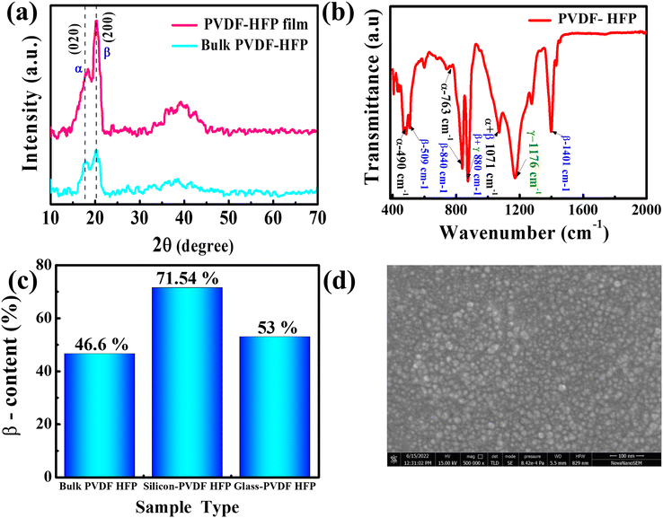 |
| | Fig. 2 Structural and phase analysis of spin-coated PVDF-HFP thin film: (a) XRD spectra, (b) FTIR spectra, (c) β-phase content, and (d) SEM image. | |
The amount of β-phase content of the PVDF-HFP thin film was measured with an attenuated total reflection Fourier transform infrared spectrometer. The following formula was used to determine the phase separation of the β-phase content (F(β)) in the film.54
| |  | (1) |
Kα and
Kβ are the absorption coefficients of the corresponding peaks, with values of 6.1 × 10
4 and 7.7 × 10
4 cm
2 mol
−1, respectively, and
Aα and
Aβ are the absorbances of the α and β phases at wavenumbers of 763 and 840 cm
−1, respectively.
Scanning electron microscopy (SEM) was used to investigate the surface morphology and microstructure of the PVDF-HFP thin film (Fig. 2(d)). In this investigation, the SEM images of the spin-coated PVDF-HFP thin film showed no discernible α-spherulitic structures (α-phase).48 This also provides additional evidence of the contribution of the electroactive β-phase in the PVDF-HFP thin film.
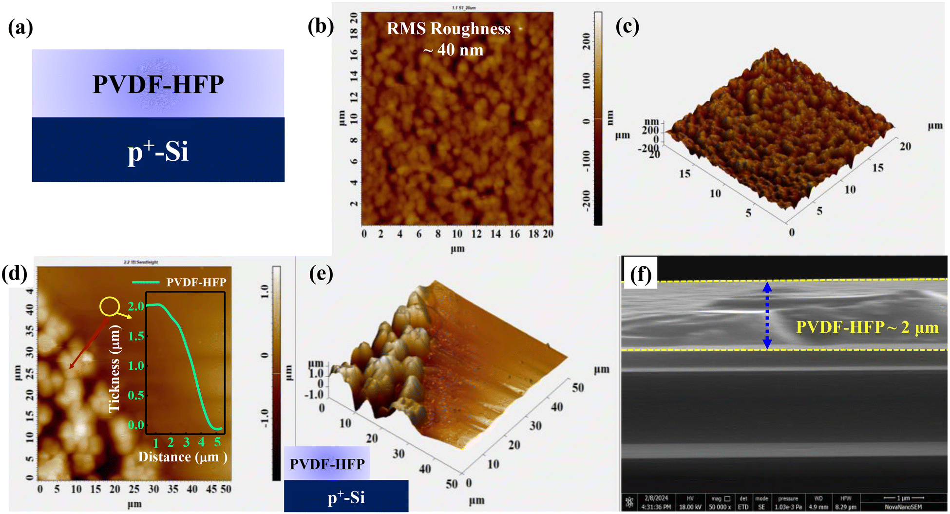
3.2. Surface morphology and thickness study of the PVDF-HFP film
The surface morphology of the PVDF-HFP thin film was examined using atomic force microscopy (AFM), and its 2D and 3D images are shown in Fig. 3(b) and (c), respectively, indicating its root mean square roughness (RRMS) of ∼40 nm, which is significantly low. This data reveals the compact nature of the PVDF-HFP thin film. Besides, its granular features arise due to the crystalline β-phase, which is discussed in the earlier sections. Moreover, the AFM study was performed on a scratched PVDF-HFP thin film to determine the PVDF-HFP film thickness. The 2D and 3D micrographs for this measurement are shown in Fig. 3(d) and (e), respectively, indicating its thickness is ∼2 μm. Besides, a cross-sectional SEM study also identified the thickness of the PVDF-HFP thin film, which is ∼2 μm (Fig. 3f).
 |
| | Fig. 3 (a) Schematic of the PVDF-HFP thin film deposited on the p+-Si substrate; (b) 2-D and (c) 3-D AFM images of the PVDF-HFP thin film surface; (d) 2-D and (e) 3-D height profile micrographs, and (f) cross-sectional FESEM image of the PVDF-HFP thin film. | |
3.3. Mechanical properties of the PVDF-HFP film on the p+-Si substrate
A nanoindentation test was performed on the PVDF-HFP thin film to measure its Young's modulus, which is strongly dependent on the substrate, processing conditions, and film thickness. The primary method of this measurement required a very small probe or indenter, which allowed it to interact with the thin film by penetrating its tip into the film to determine properties such as Young's modulus and hardness. A nanoindenter (Hysitron TI 950 TriboIndenter, Hysitron, Minneapolis, Minnesota) with a Berkovich tip and a radius of about 100 nm was used for the depth-sensing indentation experiments. The half angle between the pyramid's axis and its three faces is set at 65.35°. The tip is made of diamond, which has a Young's modulus of 1140 GPa and Poisson's ratio of 0.07. For these measurements, a load of 500 μN was employed at 50 μN s−1 with loading, holding and unloading times of 10, 20 and 10 s, respectively. The measured values of the nano hardness (h) and Young's modulus of this PVDF-HFP thin film are 74 ± 11 MPa and 1.4 ± 0.5 GPa, respectively. The typical indentation curve is shown in Fig. 4.
 |
| | Fig. 4 Load-displacement plot for PVDF-HFP/p+-Si obtained from nanoindentation. | |
3.4. Cross-sectional study of the asymmetric electrode
A cross-sectional SEM analysis was performed to determine the thickness of both the interface layers and the complete electrode, as depicted in Fig. 5. In this investigation, the LiF/Al and MoO3/Ag electrodes were prepared on a p+-Si substrate, as described in the device fabrication part. The calculated thickness of the MoO3 layer in the MoO3/Ag electrode is approximately 5 nm, and the overall thickness of the MoO3/Ag electrode is around 70 nm, with 65 nm of Al, as illustrated in Fig. 5(a). Furthermore, the overall thickness of LiF/Al is approximately 70 nm, comprising 5 nm of LiF and 65 nm of Al, as shown in Fig. 5(b).
 |
| | Fig. 5 Cross-sectional SEM images of (a) MoO3/Ag and (b) LiF/Al electrodes on the p+-Si substrate. | |
3.5. Work function analysis of electrode materials through ultraviolet photoelectron spectroscopy (UPS)
The work function of a material refers to the energy required to remove an electron from its surface. Essentially, it represents the electrostatic potential difference between electrons at the Fermi level (EF) and the maximum potential, i.e., the vacuum level. Beyond its fundamental association with the Fermi energy, the work function holds practical significance in electron emission, contact potentials, chemical reactivity, and catalysis.
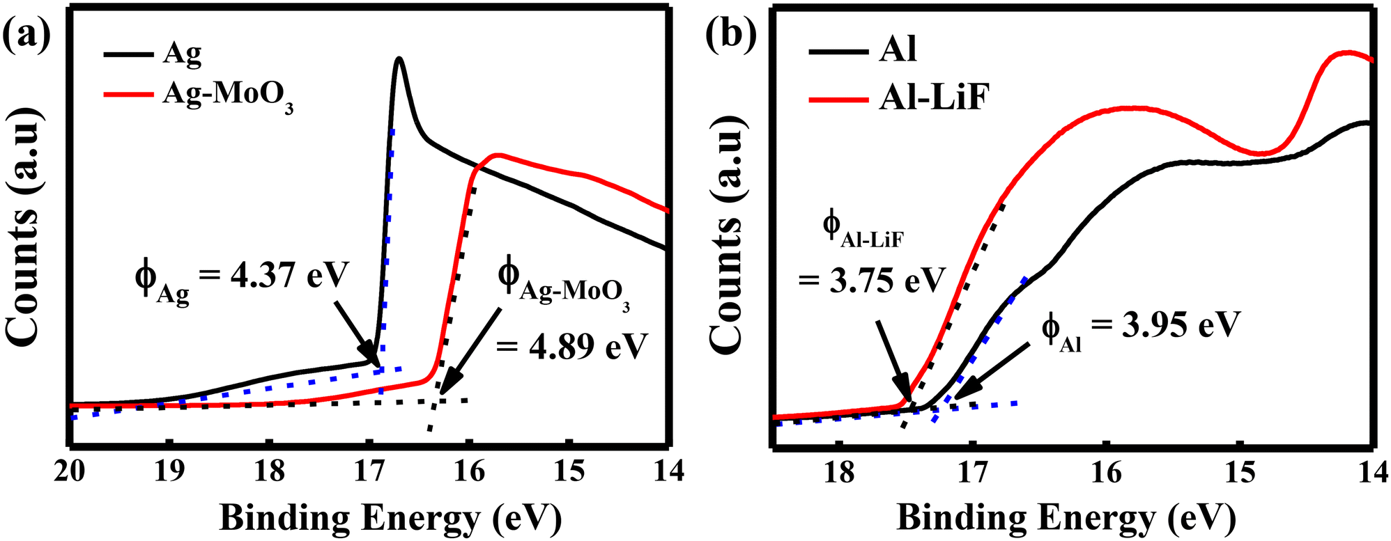
In this work, ultraviolet photoelectron spectroscopy (UPS) was used to determine the work functions of the Ag/MoO3 and LiF/Al electrodes, as shown in Fig. 6(a) and (b), respectively. For the work function study of the Ag/MoO3 electrode, the measurement was performed through a reference, cleaned Ag and Ag/MoO3 electrodes. Similarly, for the Al/LiF electrode, UPS measurements were performed on a clean Al and an Al/LiF electrode. In both cases, the photon source used was a He I discharge lamp with a photon energy of 21.22 eV. The energy scale is initially set by grounding the sample to define the kinetic energy of the Fermi edge electrons as the maximum available energy, i.e., 21.22 eV. Under these conditions, the measurement was performed, and the magnitude of the work function was calculated using the following equations.55
 |
| | Fig. 6 Secondary photoemission cutoff acquired through UPS (He I ∼ 21.22 eV), measuring the work function of the modified Ag and Al electrodes. (a) Ag and Ag–MoO3 and (b) Al and Al–LiF. | |
Fig. 6a shows the UPS spectra of Ag and Ag/MoO3, and the extracted value of the work function of Ag and Ag/MoO3 are −4.37 eV and −4.89 eV, respectively. This is in agreement with the work function of Ag and provides an indication of work function enhancement of ∼0.55 eV in the Ag/MoO3 electrode at the optimal thickness of the MoO3 layer in the Ag electrode.56 The UPS spectra of Al and Al/LiF are shown in Fig. 6b, and the work functions of Al and Al/LiF are −3.99 eV and −3.73 eV, respectively. This result suggests a decrement in the work function of the Al/LiF electrode by 0.26 eV compared to the Al electrode. This decrement in the resultant work function of Al/LiF is due to the LiF layer before the Al electrode.57,58 Therefore, the UPS-measured work function difference between MoO3/Ag and LiF/Al is −1.16 eV. However, in practical devices, the measured potential difference using the digital multimeter (KEITHLEY DMM6500 6 1/2) between the source and the drain is −0.55 V, which is still high enough to drive carriers from the channel.
3.6. Electrical characterization of the piezopotential gated self-biased transistor
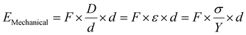
The transient current response of the device under the application of the periodic pressure is shown in Fig. 7. This measurement has been performed under zero external biasing (Vapp = 0 V) with an applied cyclic pressure of 4 bar at intervals of 5 s successively. Here, it is observed that under self-biasing (Vapp = 0 V) conditions and in the absence of applied pressure (P = 0 bar), the current level of the device is minimal (<10−9 A), but as soon as the pressure was applied on the PVDF-HFP film, the current instantly jumped to the μA level (∼10−6 A), which is more than three orders greater than initial current. This high current remains almost at the same level for that entire 5 s period of time. Such characteristics in the device have been observed due to the piezo-potential generated in the PVDF-HFP thin film under mechanical pressure, which works as a gate biasing in the device, resulting in mobile hole accumulation in the p+-Si/PVDF-HFP interface; meanwhile, the asymmetric work function of the source–drain electrodes provides negative drain biasing in the device due to their work function difference (∼−1.16 eV). The mobile charge accumulation, in combination with the potential difference of the source–drain electrodes under pressure, enhances the current level between the two electrodes. Thus, the device converts the applied mechanical energy to electrical energy under self-biasing conditions. This pattern was repeated with the applied cycle pressure, as shown in Fig. 7(a), whereas Fig. 7(b) shows the single-cycle current response under pressure off (blue region) and on conditions (red region). Furthermore, the transient response of the device featuring aluminum electrodes (symmetric electrode) was investigated, both under biasing (Vapp = 0.5 V) and self-biasing conditions (Vapp = 0 V) with 4 bar cyclic pressure, as illustrated in Fig. ESI 3(a) and (b),† respectively. Notably, the device with symmetric electrodes exhibits a 100-fold increase in current under pressure when the external bias is 0.5 V, whereas the current level remains negligible under self-biasing conditions. This observation confirms that the asymmetric work function electrode configuration of MoO3/Ag and LiF/Al, which generates ∼−0.55 V bias across the electrodes, is the primary factor in converting mechanical energy to electrical energy under self-biasing conditions. However, this mechanical-to-electrical power generation is not a continuous process. Instead, it depends on the duration of work done on the PVDF-HFP film, which is utilized to align the electric dipoles of the ferroelectric PVDF-HFP film defined by the following equation.| | | Work (W) = Force (F) × Displacement (D) | (4) |
 |
| | Fig. 7 Transient response of the device in self-biasing (V = 0 V) condition under 4 bar cyclic pressure for (a) multiple cycles and (b) single cycle. Maximum power transfer analysis (c) I–t at different resistance values (1 kΩ–10 kΩ) and (d) power vs. resistance plot of the device. | |
When D becomes zero, the applied mechanical energy will also turn to zero. However, current conduction continues for a while due to the dipole relaxation time. As a consequence, hole accumulation decreased from its peak value to zero, resulting in a steady reduction of current over time, as observed from the long-term current (I) vs. time (t) measurement (Fig. SI 5a†). For this reason, external pressure needs to be applied periodically to convert mechanical energy to electrical energy with this device. The efficiency of the device was calculated by the ratio of the input mechanical energy to the output stored electrical energy. The individual mechanical and electrical energies are calculated using eqn (5) and (6), respectively. Moreover, eqn (7) gives the conversion efficiency of the device.
| |  | (5) |
| | | EElectrical = I2 × R × Δt | (6) |
| |  | (7) |
where
F and
ε are the applied mechanical force and strain (
σ/
Y) generated in the film (
σ is the applied stress (force/area) and
Y is the Young's modulus) and
d is the thickness of the film. Moreover,
I,
R, and Δ
t are the generated current, internal resistance of the device, and time of the applied force, respectively. Apart from this, the (
EElecrical)
on and (
EElecrical)
off are the electrical energy of the device under on and off conditions, and their difference gives the stored electrical energy.
Since the device can store mechanical energy and convert it into electrical energy, the measurement was performed to extract the maximum power from the device under external load. For this purpose, variable loads are added in series to the device, ranging from 1 kΩ to 10 kΩ, and the I–t plot at different resistances is shown in Fig. 7(c). Then, the power was calculated using the formula (P = i2R), and the power vs. resistance plot is shown in Fig. 7(d). From this plot, it can be observed that the device can extract maximum power across the 4 kΩ load under such operating conditions.
Additionally, the device's repeatability was examined over an extended duration under 4 bar cyclic pressure, with 5 second intervals under self-biasing conditions. The device maintains stability for over 400 seconds (equivalent to 80 cycles), as depicted in Fig. SI 4(a) and 4(b).† The optimization of the pressure application was conducted across a range of pressures, from 1 bar to 4 bar, as illustrated in Fig. SI 5(b).† This ensures that the device yields its highest response at 4 bar. Moreover, the I–t measurement was performed under constant pressure for an extended period of time, showing exponential decay of the current, as shown in Fig. SI 5(a).† This study also indicates the current level decays to half after ∼3.5 min, implying its prolonged current generation ability.
3.7. Transistor characteristics of the device
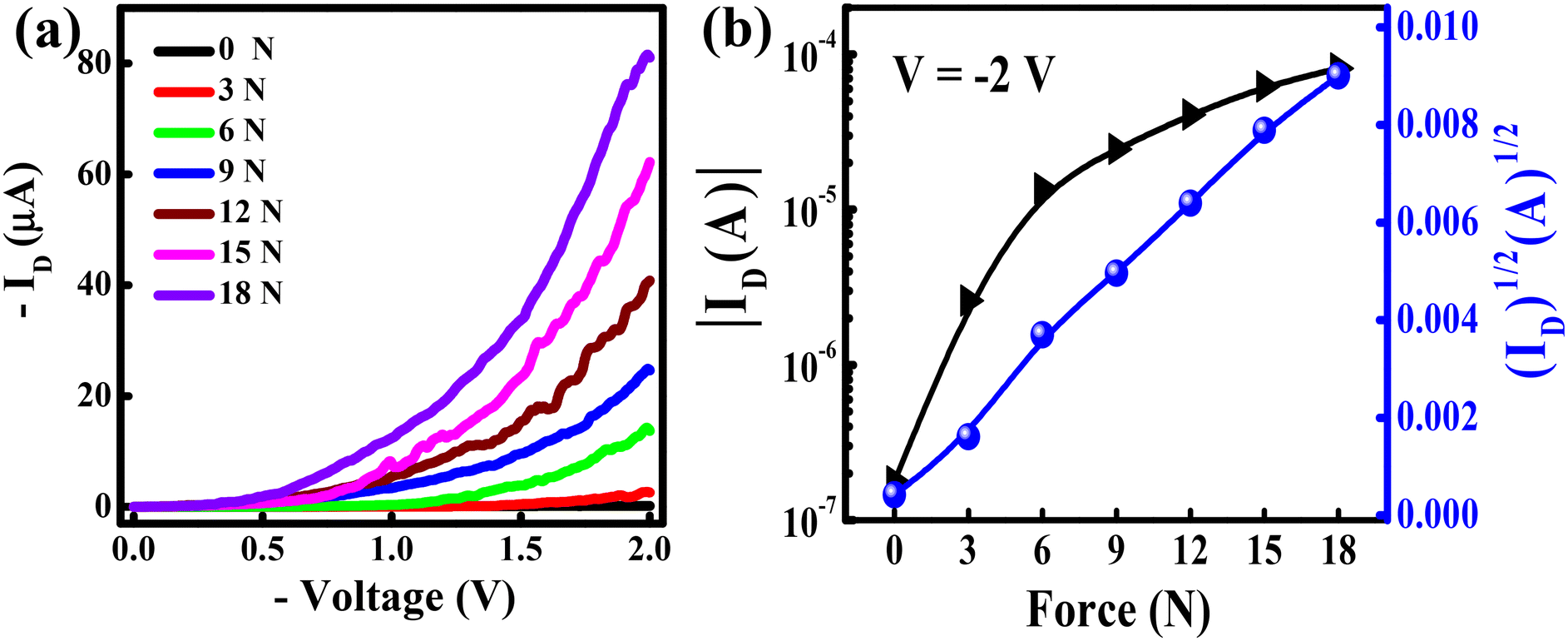
The current–voltage (I–V) measurement of the device was performed under a −2 V external bias between the electrodes under different applied forces ranging from 0 N to 18 N, with a step size of 3 N. It is observed that the magnitude of the current increases with the applied force on the device under −2 V operating voltages. The obtained characteristics under these conditions resemble the output characteristics of a p-channel transistor, as shown in Fig. 8(a), where a constant force applied to the PVDF-HFP thin film is equivalent to a constant gate bias. With these characteristics, the applied voltage between the electrodes can be considered as a drain–source voltage (VDS), while the piezo-potential is generated due to the applied force as gate voltage (VGS). The piezo-potential increases with the applied force, as the piezoelectric properties of the PVDF-HFP film facilitate the conversion of mechanical stress into an electrical potential. This piezo-potential acts as the gate potential, modulating the accumulation channel within the device. As a result, an increase in the piezo-potential enhances the drain current, reflecting the force-dependent operation of the device.
 |
| | Fig. 8
I–V characteristics of the device (a) output and (b) transfer characteristics. | |
In the same device, when the currents (I) were measured under different applied forces (0–18 N) and a constant external bias between electrodes (−2 V), the characteristics appeared similar to the transfer characteristics (ID–VG) of the p-channel transistor, as shown in Fig. 8(b). Therefore, the external force acted as a substitute for gate bias, and this device can be considered a force-induced piezopotential gated transistor. From this consideration, all the transistor parameters of the device were extracted from the transfer characteristics. The Subthreshold swing (SS) of the device was calculated using eqn (8) by extracting the slope of the log(ID) vs. VG (force) plot.59 The obtained parameters, threshold force, on–off ratio, and subthreshold swing (SS), are 0.5 N, 4.56 × 10², and 3.16 N A−1, respectively, as summarized in Table 1.
| |  | (8) |
Table 1 Summary of the transistor parameters of the device
| Device |
Threshold force (N) |
On–off ratio |
Subthreshold swing (N A−1) |
| Silicon transistor |
0.5 |
4.56 × 10² |
3.16 |
3.8. Working mechanism of the piezo-potential gated transistor
The working mechanism of the piezo-potential gated transistor is presented schematically in Fig. 9. The band diagram of the band bending due to the work function difference between LiF/Al and MoO3/Ag with respect to p+-Si is represented in Fig. SI 6.† Initially, the potential difference between the source–drain electrodes originated from the work function difference between the LiF/Al and MoO3/Ag electrodes, but the accumulated holes in the p+-Si are negligible due to the absence of any gate polarization, as schematically shown in Fig. 9(a). Under such conditions, negligibly small current flows in the device (off-state current in Fig. 7). However, as soon as external pressure is applied from the top, the piezoelectric PVDF-HFP thin film is compressed, and subsequently, a piezo-potential is generated across the PVDF-HFP film, as shown in Fig. 9(b). Since there is no significant stretching occurring along 1 or 2 directions in the device (as shown in Fig. 9), the piezoelectricity in PVDF-HFP due to d31 and d32 modes is negligible. However, due to the external force, a significant stretching occurs in the direction of 3. Therefore, the PVDF-HFP film's d33 coefficient predominates over d31 and d32, indicating that the d33 coefficient is primarily responsible for the piezo-potential.60,61 Since the PVDF-HFP layer is laminated on top of the p-type silicon (p+-Si), dipoles in the PVDF-HFP under compression are aligned in such a way that creates a negative potential at the bottom layer of the PVDF-HFP, i.e., at the interface of PVDF-HFP/p+-Si as reported earlier.52,62 This negative piezo potential in PVDF-HFP facilitates the accumulation of holes in the top layer of p+-Si, which results in the formation of a conducting channel. The associated energy band and charge accumulation, both without and with pressure, are shown schematically in Fig. SI 6(a) and (b),† respectively. Thus, a conducting channel of holes was created. These mobile holes can move through the channel under the driving potential generated due to the work function difference between the LiF/Al and MoO3/Ag electrodes.63–65 Hence, a significant enhancement in the current was obtained in the I–t plot even without any external voltage. When the pressure was removed from the piezoelectric layer, the polarized dipoles try to regain their initial state. However, this reorientation of dipoles takes a relatively longer time. After removing the pressure from the PVDF-HFP film, the dipoles reorient in opposite polarity for a short time, with a much smaller magnitude, before attaining the relaxed state, as shown in Fig. 9(c).
 |
| | Fig. 9 Working mechanism of the piezo-potential self-biased transistor under (a) normal state, (b) stressed state and (c) relaxed state. | |
Therefore, it creates a strong depletion region at the PVDF-HFP/p-Si+ interface, resulting in a quick turn-off of channel conduction. This process is repeated in consecutive cycles of applied pressure in a similar manner, as realized in the I–t plot (Fig. 7). As the applied force on the device is raised from 0 N to 18 N, the piezo potential increases proportionally, which acts as the gate bias of the device, leading to a proportional augmentation in the magnitude of the drain current, as shown in Fig. 8(b), which is equivalent to the transfer characteristics of a transistor.
4. Conclusion
In conclusion, a piezo-potential self-biased transistor was fabricated on a heavily doped silicon (p+-Si) (111) substrate and used as a mechanical energy harvesting device, which efficiently converts mechanical energy to electrical energy. The self-bias nature of this top-gated transistor was achieved by developing two voltage sources in its device design. For developing the drain bias, asymmetric work function electrodes were used in the source and drain. Specifically, LiF/Al and MoO3/Ag are used as the source and drain electrodes, respectively, with a work function difference of ∼−1.16 V (measured by UPS), which serves as the driving voltage of the channel. In addition, a piezoelectric PVDF-HFP layer was used as a gate dielectric on which external pressure was applied. Under pressure, the PVDF-HFP layer deforms and generates a polarization that works as a gate bias of the device. Due to gate polarization, holes accumulate on the top layer of p+-Si, conducting between the source and drain electrodes due to the work function difference between the source and drain. The maximum power conversion efficiency of this device depends on the external pressure, and it reaches ∼75% under 4 bar external pressure. To the best of our knowledge, this is one of the highest reported efficiencies for a mechanical energy harvesting device, which is made possible by its unique design and working principle. Besides, this device shows electrical characteristics equivalent to a transistor where the gate bias is replaced by external forces. By considering this device as a force-induced piezopotential gated transistor, the extracted device parameters, including the threshold force, on–off ratio, and subthreshold swing (SS) are 0.5 N, 4.56 × 10², and 3.16 N A−1, respectively.
Data availability
Data is available in the following link in OBJ format. https://drive.google.com/drive/folders/19UkuzWvr3NR9SOJc82wMJHD5Rdiyvp1Y?usp=drive_link.
Conflicts of interest
The authors declare no conflict of interest.
Acknowledgements
Bhola Nath Pal thanks SERB, India (CRG/2019/001826) and DST, India (DST/INT/SWD/VR/P-12/2019) for financial support. The authors are also grateful to the Central Instrument Facility Centre, IIT (BHU) for providing instrument support for AFM, UPS, and FESEM. The authors acknowledge DST-FIST (SR/FST/ET-II/2018/277(C)) for providing GIXRD/XRD instrument facility. Utkarsh Pandey, Nila Pal, Sandeep Dhaiya, and Sobhan Hazra appreciate IIT (BHU) for sponsoring the SRF scholarship. The authors further thank Prof. Pijush Ghosh (Department of Applied Mechanics, Indian Institute of Technology Madras) for providing the Nanoindentation facility.
References
- T. W. Brown, T. Bischof-Niemz, K. Blok, C. Breyer, H. Lund and B. V. Mathiesen, Renewable Sustainable Energy Rev., 2018, 92, 834–847 CrossRef.
- M. Z. Jacobson, M. A. Delucchi, Z. A. Bauer, S. C. Goodman, W. E. Chapman, M. A. Cameron, C. Bozonnat, L. Chobadi, H. A. Clonts and P. Enevoldsen, Joule, 2017, 1, 108–121 Search PubMed.
- C. Kumar, A. Gaur, S. K. Rai and P. Maiti, Nano-Struct. Nano-Objects, 2017, 12, 174–181 CAS.
- T. Li and P. S. Lee, Small Struct., 2022, 3, 2100128 CAS.
- Z. Yang, S. Zhou, J. Zu and D. Inman, Joule, 2018, 2, 642–697 CrossRef CAS.
- N. Sezer and M. Koç, Nano Energy, 2021, 80, 105567 CrossRef CAS.
-
K. Uchino, Advanced piezoelectric materials: Science and technology, Woodhead Publishing, 2017 Search PubMed.
- F. Narita and M. Fox, Adv. Eng. Mater., 2018, 20, 1700743 CrossRef.
- S. R. Anton and H. A. Sodano, Smart Mater. Struct., 2007, 16, R1 CrossRef CAS.
- Y. Zhang, M. Xie, J. Roscow, Y. Bao, K. Zhou, D. Zhang and C. R. Bowen, J. Mater. Chem. A, 2017, 5, 6569–6580 RSC.
- H. Park, C. Ha and J.-H. Lee, J. Mater. Chem. A, 2020, 8, 24353–24367 RSC.
- D. Lin, W. Zhang, H. Yin, H. Hu, Y. Li, H. Zhang, L. Wang, X. Xie, H. Hu and Y. Yan, Research, 2022, 2022, 9820585 CAS.
- X. Wan, H. Cong, G. Jiang, X. Liang, L. Liu and H. He, ACS Appl. Nano Mater., 2023, 6, 1522–1540 CrossRef CAS.
- S. Sukumaran, S. Chatbouri, D. Rouxel, E. Tisserand, F. Thiebaud and T. Ben Zineb, J. Intell. Mater. Syst. Struct., 2021, 32, 746–780 Search PubMed.
- C. Wan and C. R. Bowen, J. Mater. Chem. A, 2017, 5, 3091–3128 RSC.
- C. R. Bowen, J. Taylor, E. LeBoulbar, D. Zabek, A. Chauhan and R. Vaish, Energy Environ. Sci., 2014, 7, 3836–3856 RSC.
- C.-C. Hong, S.-Y. Huang, J. Shieh and S.-H. Chen, Macromolecules, 2012, 45, 1580–1586 CrossRef CAS.
- M. Li, H. J. Wondergem, M.-J. Spijkman, K. Asadi, I. Katsouras, P. W. Blom and D. M. De Leeuw, Nat. Mater., 2013, 12, 433–438 CrossRef CAS PubMed.
- Y. Wu, Y. Ma, H. Zheng and S. Ramakrishna, Mater. Des., 2021, 211, 110164 CrossRef CAS.
- P. Saxena and P. Shukla, Adv. Compos. Hybrid Mater., 2021, 4, 8–26 CrossRef CAS.
- R. S. Kumar, T. Sarathi, K. Venkataraman and A. Bhattacharyya, Mater. Lett., 2019, 255, 126515 CrossRef.
- B. Chai, K. Shi, Y. Wang, Y. Liu, F. Liu, P. Jiang, G. Sheng, S. Wang, P. Xu and X. Xu, Nano Lett., 2023, 23, 1810–1819 CrossRef CAS PubMed.
- C. Chang, V. H. Tran, J. Wang, Y.-K. Fuh and L. Lin, Nano Lett., 2010, 10, 726–731 CrossRef CAS PubMed.
- V. Singh, D. Meena, H. Sharma, A. Trivedi and B. Singh, Energy, 2022, 239, 122125 CAS.
- S. K. Karan, D. Mandal and B. B. Khatua, Nanoscale, 2015, 7, 10655–10666 CAS.
- D. Bhattacharya, S. Bayan, R. K. Mitra and S. K. Ray, Nanoscale, 2021, 13, 15819–15829 CAS.
- Q. Zhu, X. Song, X. Chen, D. Li, X. Tang, J. Chen and Q. Yuan, Nano Energy, 2024, 127, 109741 CAS.
- Y. He, H. Wang, Z. Sha, C. Boyer, C.-H. Wang and J. Zhang, Nano Energy, 2022, 98, 107343 CAS.
- H. Liu, J. Zhong, C. Lee, S.-W. Lee and L. Lin, Appl. Phys. Rev., 2018, 5, 041306 Search PubMed.
- X. Yuan, X. Gao, J. Yang, X. Shen, Z. Li, S. You, Z. Wang and S. Dong, Energy Environ. Sci., 2020, 13, 152–161 CAS.
- A. Toprak and O. Tigli, Appl. Phys. Rev., 2014, 1, 031104 Search PubMed.
- J. Xu, X. Wang, C. Wang, L. Yuan, W. Chen, J. Bao, Q. Su, Z. Xu, C. Wang and Z. Wang, Adv. Mater., 2021, 33, 2000893 CAS.
- S.-G. Kim, S. Priya and I. Kanno, MRS Bull., 2012, 37, 1039–1050 CAS.
- J. Chen, Y. Huang, N. Zhang, H. Zou, R. Liu, C. Tao, X. Fan and Z. L. Wang, Nat. Energy, 2016, 1, 1–8 CAS.
- E. Jiaqiang, B. Luo, D. Han, J. Chen, G. Liao, F. Zhang and J. Ding, Energy, 2022, 239, 122509 Search PubMed.
- R. Bogue, Sens. Rev., 2013, 33, 300–304 Search PubMed.
- F. Ejeian, S. Azadi, A. Razmjou, Y. Orooji, A. Kottapalli, M. E. Warkiani and M. Asadnia, Sens. Actuators, A, 2019, 295, 483–502 CAS.
-
M. Gardos, Advantages and Limitations of Silicon as a Bearing Material for MEMS Applications, 1998, pp. 341–365.
- D. K. Kashyap, A. K. Srivastava and M. K. Gupta, ACS Appl. Electron. Mater., 2024, 6, 862–874 CrossRef CAS.
- E. J. Lee, T. Y. Kim, S.-W. Kim, S. Jeong, Y. Choi and S. Y. Lee, Energy Environ. Sci., 2018, 11, 1425–1430 RSC.
- N. Soin, T. H. Shah, S. C. Anand, J. Geng, W. Pornwannachai, P. Mandal, D. Reid, S. Sharma, R. L. Hadimani, D. V. Bayramol and E. Siores, Energy Environ. Sci., 2014, 7, 1670–1679 RSC.
- M. Morita, T. Ohmi, E. Hasegawa, M. Kawakami and M. Ohwada, J. Appl. Phys., 1990, 68, 1272–1281 CrossRef CAS.
- U. Pandey, N. K. Chourasia, N. Pal, S. Biring and B. N. Pal, IEEE Trans. Electron Devices, 2022, 69, 1077–1082 CAS.
- U. Pandey, A. K. Yadav, N. Pal, P. K. Aich and B. N. Pal, J. Mater. Chem. C, 2023, 11, 15276–15287 RSC.
- K. Muhieddine, M. Ullah, B. N. Pal, P. Burn and E. B. Namdas, Adv. Mater., 2014, 26, 6410–6415 CrossRef CAS PubMed.
- M. Kundu, D. Mondal, N. Bose, R. Basu and S. Das, ACS Appl. Nano Mater., 2024, 7, 1804–1814 CrossRef CAS.
- S. Ghosh, D. Mondal, S. Roy, J. Roy, S. Bardhan, A. Mazumder, N. Bag, R. Basu and S. Das, J. Mater. Chem. C, 2023, 11, 13418–13428 RSC.
- R. Mishra, S. K. Singh, H. Gupta, R. K. Tiwari, D. Meghnani, A. Patel, A. Tiwari, V. K. Tiwari and R. K. Singh, Energy Fuels, 2021, 35, 15153–15165 CrossRef CAS.
- H. Shaik, S. Rachith, K. Rudresh, A. S. Sheik, K. Thulasi Raman, P. Kondaiah and G. Mohan Rao, J. Polym. Res., 2017, 24, 1–6 CrossRef CAS.
- S. Ramasundaram, S. Yoon, K. J. Kim and J. S. Lee, Macromol. Chem. Phys., 2008, 209, 2516–2526 CrossRef CAS.
- B. Mahale, D. Bodas and S. Gangal, Bull. Mater. Sci., 2017, 40, 569–575 CrossRef CAS.
- I. Y. Abdullah, M. Yahaya, M. H. H. Jumali and H. M. Shanshool, Surf. Rev. Lett., 2016, 23, 1650005 CrossRef.
- U. Pandey, N. Pal, V. Acharya, P. K. Aich, A. K. Yadav and B. N. Pal, IEEE Sens. J., 2023, 23, 11482–11489 CAS.
- S. Wang, W. Tong, Y. Li, P. Zhang, Y. Liu, Y. Chen and Y. Zhang, Nano Energy, 2023, 105, 108026 CrossRef CAS.
- J. W. Kim, A. Kim, H. U. Hwang, J. H. Kim, S. Choi, N. Koch, D. Shin, Z. Zhao, F. Liu and M. Choi, J. Vac. Sci. Technol., A, 2023, 41, 053211 CrossRef CAS.
- W. Sun, J. K. Jha, N. D. Shepherd and J. Du, Comput. Mater. Sci., 2018, 141, 162–169 CrossRef CAS.
- T. Brown, R. Friend, I. Millard, D. Lacey, J. Burroughes and F. Cacialli, Appl. Phys. Lett., 2000, 77, 3096–3098 CrossRef CAS.
- C. J. Brabec, S. E. Shaheen, C. Winder, N. S. Sariciftci and P. Denk, Appl. Phys. Lett., 2002, 80, 1288–1290 CrossRef CAS.
- H. H. Choi, K. Cho, C. D. Frisbie, H. Sirringhaus and V. Podzorov, Nat. Mater., 2018, 17, 2–7 CrossRef CAS PubMed.
-
C. Baur, D. J. Apo, D. Maurya, S. Priya and W. Voit, in Polymer composites for energy harvesting, conversion, and storage, ACS Publications, 2014, pp. 1–27 Search PubMed.
- H. Guo, J. Wan, H. Wu, H. Wang, L. Miao, Y. Song, H. Chen, M. Han and H. Zhang, ACS Appl. Mater. Interfaces, 2020, 12, 22357–22364 CrossRef CAS PubMed.
- S. Roy, P. Thakur, N. A. Hoque, B. Bagchi and S. Das, RSC Adv., 2016, 6, 21881–21894 RSC.
- P. K. Aich, Z. Genene, U. Pandey, A. K. Yadav, E. Wang and B. N. Pal, ACS Photonics, 2024, 11, 3704–3712 CrossRef CAS.
- S. Dahiya, U. Pandey, S. Hazra, R. Chakraborty, S. Pramanik, P. P. Maurya and B. N. Pal, Adv. Mater. Technol., 2024, 2401532 Search PubMed.
- S. Dahiya, S. Hazra, U. Pandey, S. Pramanik, P. Dahiya, S. V. Singh, N. Kumari and B. N. Pal, Opt. Mater., 2024, 157, 116182 CrossRef CAS.
|
| This journal is © The Royal Society of Chemistry 2025 |
Click here to see how this site uses Cookies. View our privacy policy here. 
 Open Access Article
 This Open Access Article is licensed under a Creative Commons Attribution-Non Commercial 3.0 Unported Licence
 ,
Nila
Pal
,
Sandeep
Dahiya
,
Nila
Pal
,
Sandeep
Dahiya