
 Open Access Article
 This Open Access Article is licensed under a
 Creative Commons Attribution 3.0 Unported Licence
Magnetoelastic anisotropy drives localized magnetization reversal in 3D nanowire networks†
Laura G.
Vivas
 *a,
Alejandra
Ruiz-Clavijo
a,
Olga
Caballero-Calero
a,
David
Navas
b,
Amanda A.
Ordoñez-Cencerrado
c,
Cristina V.
Manzano
a,
Ruy
Sanz
c and
Marisol
Martín-González
*a
*a,
Alejandra
Ruiz-Clavijo
a,
Olga
Caballero-Calero
a,
David
Navas
b,
Amanda A.
Ordoñez-Cencerrado
c,
Cristina V.
Manzano
a,
Ruy
Sanz
c and
Marisol
Martín-González
*a
aInstituto de Micro y Nanotecnología, IMN-CNM, CSIC (CEI UAM+CSIC) Isaac Newton, 8, Tres Cantos, Madrid E-28760, Spain. E-mail: laura.g.vivas@csic.es; Marisol.martin@csic.es
bInstituto de Ciencia de Materiales de Madrid, CSIC, Cantoblanco, 28049 Madrid, Spain
cNational Institute for Aerospace Technology (INTA), Space Payloads Department, Torrejón de Ardoz, Madrid 28850, Spain
First published on 14th January 2025
Abstract
Three-dimensional magnetic nanowire networks (3DNNs) have shown promise for applications beyond those of their linear counterparts. However, understanding the underlying magnetization reversal mechanisms has been limited. In this study, we present a combined experimental and computational investigation on simplified 3DNNs to address this gap. Our findings reveal a previously unidentified in-plane magnetoelastic anisotropy, validated through comparisons between experimental and simulated magnetic data. Notably, we discovered that magnetization reversal in 3DNNs is driven by highly localized magnetic states, arising from the interplay of exchange and dipolar interactions, magnetoelastic anisotropy, and nanowire microstructure. This discovery challenges the prevailing understanding of magnetization reversal in nickel nanowires. Our work provides critical insights into the magnetic behavior of 3DNNs, opening doors for their tailored design and optimization.
Introduction
The emergence of three-dimensional (3D) metamaterials from their linear electromagnetic counterparts two decades ago,1 ignited a revolution in material science. Since then, research has unveiled a diverse range of systems exhibiting properties exceeding the sum of their individual components. These systems encompass a broad spectrum of functionalities, including magnetic,2 optical,3,4 thermoelectric efficiency,5,6 mechanical,7 plasmonics8 and acoustic properties.9 Magnetic 3D metamaterials offer multiple scenarios to explore fundamental phenomena.10,11 Their ability to sustain long-range magnetic order throughout the structure facilitates the emergence of complex spin textures, opening exciting avenues for the development of multifunctional technologies in nanoelectronics,12,13 sensing14 and medicine.15 Further, the precise control of their magnetic features offers immense potential in various fields such as magnetic recording,16,17 microwave devices18,19 and space technology.20,21Magnetic three-dimensional nanowire networks (3DNNs) stand out as a promising class of material for crafting intricate 3D nanoarchitectures, enabling the creation of more complex and functional nanoscale structures with tailored functionalities. The interconnected nature of these networks, formed by individual nanowires (NWs), allows them to simultaneously accommodate domain walls for compact information storage and spin waves for energy-efficient communication. Furthermore, 3DNNs are actively explored for their potential in energy storage22 and brain-inspired computing, where they mimic neurons, with the constrictions between NWs functioning as neural synapses.23 These diverse applications hinge on a critical factor: the interplay between various magnetic anisotropies inherent to these 3D nanostructures.24 Magnetic anisotropy has been demonstrated to be key for the stabilization of magnetic textures,25 the fundamental building blocks of information storage and logic devices.26,27 This principle underpins a wide range of magnetic applications, extending to power generation and hybrid electric vehicles.28
A significant breakthrough in obtaining 3D nanostructures has been achieved by the demonstration of versatile, easy to scale and controlled fabrication of interconnected NWs networks by electrodeposition in self-assembled 3D nanoporous templates.29–31 Indeed, polycarbonate etched ion-track17,18 and anodic aluminium oxide (AAO) templates have been actively used for the fabrication of interconnected or cross-connected 3D magnetic nanostructures.32,33 While polycarbonate templates result in random networks of interconnected nanowires at varying angles, AAO templates offer superior control, producing parallel nanowires arranged in a well-defined hexagonal pattern with interconnections produced by orthogonal nanowires connecting each nanowire to each six closer neighbors. And the inter-distance between those transversal connecting nanowires can be modulated as desired, as so their shape.34 Due to their higher controlled ordering, these latter patterns are more promising for technological applications. Previous works on 3DNNs have demonstrated that the addition of transversal nanowires (TNWs) strongly modify the symmetry of the global magnetic response in comparison to non-interconnected NWs.18,32,35 In particular, experiments on nickel (Ni), cobalt (Co) and NiCo alloys have suggested that a low density of TNWs barely affects the effective global anisotropy, whereas a high density promotes a rotation from the out-of-plane to in-plane, opening the door to tailoring magnetic anisotropy at will.32,35 However, precise understanding of the key parameters determining this anisotropy reorientation by the addition of TNWs has been hampered by computational limitations17,36 since these previous works have studied 3DNNs with nanowires of tens of micrometers, with tens of equally spaced TNWs.
In this work, we address the current limitations in understanding the magnetic behavior of 3DNNs by conducting a combined experimental and computational study on simplified Ni 3DNNs featuring a single interconnection. Our approach enables us to uncover the microscopic origin of the observed anisotropy reorientation and, crucially, reveal an in-plane magnetoelastic anisotropy that plays a pivotal role in the magnetization reversal process. Our findings reveal the emergence of a magnetoelastic anisotropy at the nanograin level within the nanostructure, whose orientation shifts from out-of-plane to in-plane due to the incorporation of TNWs. As a consequence, the predicted magnetization reversal pathway occurs through highly localized magnetic states arising from the interplay between exchange interaction, magnetoelastic random anisotropy, and nanowire microstructure, specifically crystallite size. This challenges the conventional understanding of magnetization reversal in nickel nanowires based on delocalized modes.37
Results and discussion
Fig. 1(a) shows a scanning electron microscope (SEM) image of the cross-section of the investigated nickel 3DNNs composed of parallel cylindrical nanowires of 1250 ± 20 nm length, 55 ± 5 nm radius with an inter-wire distance of 65 nm and with a single transverse connection located at 770 ± 20 nm from the bottom [see Methods for a detailed description]. For comparison, we also investigate nickel nanowires without TNWs. Fig. 1(b) shows the X-Ray diffraction (XRD) spectra of both systems, with and without transverse nanowires. One can observe that the addition of transverse nanowires adds a crystallographic texture in the polycrystalline nickel along the [220] orientation (Fig. 1(b) top) which is absent in the NWs (Fig. 1(b) bottom). The magnetic characterization is performed using both a vibrating sample magnetometer (VSM) for angle-dependent hysteresis loops and a SQUID for temperature-dependent hysteresis loops [see Methods for a detailed description]. Fig. 2(a) shows the virgin or first magnetization curves after a demagnetization process and recorded by applying the external field at four different angles, including perpendicular (in-plane, IP, in reference to the surface of the whole sample) and parallel (out-of-plane, OOP) to the axis of the longitudinal nickel nanowires.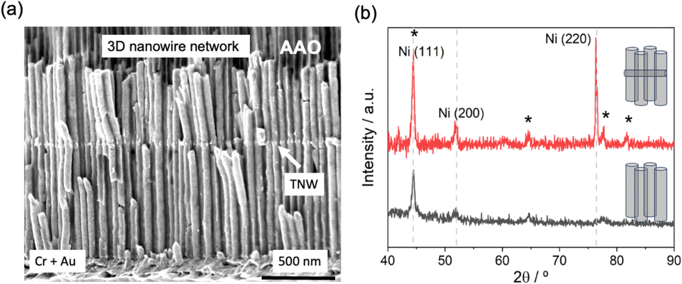 | ||
| Fig. 1 (a) Scanning electron microscope (SEM) image of the cross-section of the nickel 3D nanowire network (3DNN). These networks comprise parallel nanowires with an average length of 1250 ± 20 nm and a single transverse nanowire positioned 770 ± 20 nm from the bottom. For comparison, we also studied nickel nanowire networks without transverse nanowires. (b) Top XRD pattern corresponds to the nickel 3DNN in AAO template in (a), while the bottom XRD pattern corresponds to Ni nanowires without transverse nanowires fabricated under similar conditions. | ||
 | ||
| Fig. 2 First magnetization curves for nickel 3D nanowire networks for four different angles, longitudinal to the nanowire axis 90° (or OOP), at 30° and 60°, and perpendicular to the nanowire axis 0° (or IP) for (a) measured and (b) gained from micromagnetic simulations. | ||
In a first step, information about the effective global anisotropy energy Keff that defines the magnetic energy landscape can be determined as the difference between the magnetic energies needed to saturate the sample measured along the hard and easy directions of magnetization. By defining, mIP and mOOP as the normalized initial magnetization curves, perpendicular and parallel to the axial direction, respectively, then38
 | (1) |
First, the standard bulk value of the magnetocrystalline cubic anisotropy for Ni, Kc = −4.85 × 10³ J m−3,39 is lower than the observed effective anisotropy. Moreover, due to the polycrystalline character of the nanowires it is common to assume that the directions of the anisotropy axes vary randomly for each crystalline grain (20 nm average size from XRD cf. Fig. 1(b)). Hence, in such polycrystalline nickel samples, the contribution of the magnetocrystalline anisotropy to the total effective anisotropy tends to average out to zero.
For a single, homogeneously magnetized nanowire, the shape anisotropy Ksh = πMs2 = 7.5 × 10⁴ J m−3. This value corresponds to a uniaxial anisotropy along the nanowire axis favouring magnetization along the OOP direction. This contribution has opposite orientation compared to the observed effective anisotropy. Determining the contribution of dipolar interactions between closely packed magnetic nanowires with a simple expression is highly challenging. The literature proposes various expressions for this contribution, such as Kms ∼ −πMs23P,40 where P represents for the sample's porosity or filling factor. We can determine the nominal value of the filling factor in our samples, P ≈ 0.65, using the relation  ,41 where d = 55 nm is the pore's diameter and dcc = 65 nm the center-to-center distance of neighbouring pores. By using this estimation, the dipolar interaction-related anisotropy for our sample would be Kms = −1.5 × 10⁵ J m−3, one order of magnitude larger than the observed effective anisotropy (Keff = −1.76 × 10⁴ J m−3). This discrepancy could be attributed to several causes, including partially filled pores, the variation of the geometrical parameters, or the presence of highly non-uniform magnetic states.39
However, to truly determine the origin of the effective anisotropy of the Ni 3DNNs one needs to go beyond macroscopic approximations and resort to micromagnetic models that accurately account for the interplay between energy contributions, including anisotropies and dipolar interactions.42–44 We achieve this with a systematic computational investigation using a realistic micromagnetic model that considers the geometric structure and microstructural composition, and explores the optimal magnetic parameters that characterize the magnetic response of the 3DNNs [see Methods for a detailed description].
In the first step, we verify that micromagnetic simulations of angle-dependent first magnetization curves, using a model that includes magnetocrystalline, shape, and dipolar interactions, do not accurately reproduce the experimental observations [see section S1 of ESI†]. This model has been used previously for the modelling of the magnetic hysteresis of magnetic 3DNNs.32,35 However, in nickel NWs one needs to account for the magnetostriction, which leads to a significant magnetoelastic (ME) contribution to the effective anisotropy along the nanowire axis in quasi-crystal nanowires (Kme = 1.9–8.2 × 10⁴ J m−3)38 and perpendicular to it (Kme = −1 × 10⁴ J m−3)45 for polycrystalline nanowires. Magnetoelastic anisotropy appears in the nickel nanowires due to the mechanical interaction between substrate, the alumina template and the nanowires, arising from internal thermal stresses and the large magnetostriction of nickel.46–49 Upon cooling, such as after electrodeposition, the nanowires experience lateral compressive stress due to the significant mismatch in the thermal expansion coefficients of alumina, the substrate, and nickel. Previous studies have interpreted this effect, based on micromagnetic models, as a reduction in the effective anisotropy along the nanowire's longitudinal axis, equivalent to a hard-axis anisotropy along the nanowire. However, this approach overlooks the randomness of ME anisotropy at the crystallite level (with an average size of 20 nm, Fig. 1(b)). Moreover, these models often oversimplify the actual geometry and structural characteristics of nanowires, as well as the complexities involved in realistic magnetostatic energy calculations.
In this work, we move beyond these limitations by conducting micromagnetic simulations that incorporate a random ME anisotropy term, Kme, at the crystallite level. By systematically exploring the simulation parameter space [refer to section S2 and S3 of ESI†], we achieve optimal agreement between the model and experimental observations. This agreement occurs with a ME anisotropy value of Kme = 7 × 10⁴ J m−3, where each crystallite has a randomly oriented in-plane (IP) anisotropy. We note that the ME anisotropy value is taken as positive, which is not in contradiction with the convention of using negative values for hard-axis (or easy-plane) anisotropy. This is because we have considered an easy-axis ME anisotropy acting at each crystallite, rather than a hard-axis anisotropy. The randomness of the ME anisotropy direction averages to zero, implying no preferred in-plane orientation, but it penalizes out-of-plane orientations. Fig. 2(b) shows the micromagnetic calculations of the first magnetization curves for four different magnetic field angles, demonstrating excellent agreement with the experimental results (Fig. 2(a)).
Fig. 3 shows both the experimentally measured and the micromagnetically calculated angle-dependent hysteresis loops for the same four angle orientations. The remarkable agreement between experimental data (Fig. 3(a)) and micromagnetic modelling (Fig. 3(b)) across all angles underscores the validity of our approach. Interestingly, the contribution of dipolar interactions between nanowires to the overall anisotropy can be estimated by subtracting the in-plane ME and shape anisotropies from the experimentally measured effective global anisotropy (refer to eqn (1) and Fig. 2). This analysis reveals that the dipolar interactions contribute with an effective in-plane anisotropy of Kms ≈ −2.25 × 10⁴ J m−3. The experimentally obtained value is smaller than the theoretical expectation. In the literature, this reduction is attributed to local anisotropies caused by defects and finite dimensions, which result in a multidomain structure and, consequently, localized reversal.50,51 Unlike previous studies, we demonstrate that the localized multidomain structure is driven by random magnetoelastic anisotropy at the crystallite level. The formation of such a structure reduces the saturation magnetization, Ms, and, as a result, lowers the dipolar interaction anisotropy constant.52
 | ||
| Fig. 3 Hysteresis loops of nickel 3D nano-networks for four different angles, perpendicular to the nanowire axis 0° (IP), at 30° and 60°, and longitudinal to the nanowire axis 90° (OOP). (a) Measured hysteresis loops and (b) from micromagnetic simulations. | ||
Magnetization reversal occurs through highly localized magnetic states
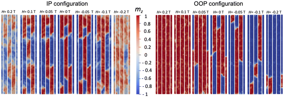
Fig. 4 reveals a striking feature of the magnetization reversal in 3DNNs: it proceeds through highly localized magnetic states, a phenomenon not previously observed in nickel nanowire networks. This localized reversal, arising from the interplay of exchange interaction, magnetoelastic random anisotropy, and nanowire microstructure, challenges the prevailing understanding of reversal mechanisms based on delocalized modes. | ||
| Fig. 4 Magnetic configurations during reversal for the OOP configuration with a magnetic external field along the axial direction of a slice of the central nanowires in our micromagnetic model at various magnetic field strengths around remanence. (Top panel) Micromagnetic configurations of the mz component. (Bottom panel) Micromagnetic configurations of the mx component. | ||
Fig. 4 provides the micromagnetic configurations at different stages of the reversal pathway in a slice of the central nanowires of the 3DNNs for the OOP configuration (see Fig. 3). The magnetization component along the nanowire axis (mz) initiates reversal through localized nucleation of magnetic domains along the nanowire length. Established theories and micromagnetic simulations suggest that, in nickel nanowires, there are three primary reversal mechanisms: coherent rotation, transverse domain wall, and vortex domain wall modes. These are classified as delocalized modes because they extend throughout the nanowires.37 Typically, the magnetization reversal process occurs through the nucleation of domain walls or vortex states at the ends of a nanowire, followed by depinning and propagation along its length. This reversal occurs wire-by-wire rather than cooperatively, aligning with interpretations used in previous studies of magnetic 3DNNs.32,35 Therefore, our observations of highly localized magnetization during reversal challenge the established understanding that magnetization reversal in nickel nanowires occurs through delocalized modes.35,37
To elucidate the origin of our results, we employ a phenomenological magnetic localization theory for reversal in transition-metal nanowires based on a random-anisotropy model.53 This theory shows that even a small amount of disorder can lead to localization, with the degree of localization strongly dependent on the nanowire's nanostructure. The localization length can be determined as R* ∼δ40/R30, where R0 = 20 nm is the crystallite size and  the wall-width parameter, where Kgrain stands for grain's average anisotropy and Aex the exchange stiffness constant [see Methods for value].
Estimating the average anisotropy within each crystallite is challenging because the lack of simple analytical expressions for such non-homogeneous magnetic states. Similar to the case of Kms, its value is lower than that for the homogeneous case. Using the effective anisotropy determined from the analysis of the first magnetization curves, Keff = Kme + Kms + Ksh = −1.76 × 10⁴ J m−3, the theory estimates the localization length to be approximately R* ∼5 nm. Notably, theory predicts a three-dimensional non-cooperative regime when δ0/R0 < 1 and R/R0 > 1, where R = 27.5 nm is the nanowires radius. In this regime, localized magnetization regions reverse incoherently, aligning with our micromagnetic simulations (cf.Fig. 4).
Similarly, Fig. 5 illustrates the localized magnetic states in a slice of the central nanowires for the in-plane (IP) configuration. In this case, reversal iniciates at lower fields compared to the out-of-plane (OOP) configuration (see Fig. 3) due to the in-plane anisotropic contributions from dipolar interactions and magnetoelastic anisotropy. The top panel of Fig. 5 displays the spatial evolution of the mz component for the IP configuration. The color code indicates that the switching pathways are primarily confined to the x- and y-components of the magnetization, due to the strong energy penalty from in-plane magnetoelastic anisotropy.
 | ||
| Fig. 5 Magnetic configurations during reversal for the IP configuration with a magnetic external field perpendicular to the axial direction of a slice of the central nanowires in our micromagnetic model at various magnetic field strengths around remanence. (Top panel) Micromagnetic configurations of the mz component. (Bottom panel) Micromagnetic configurations of the mx component. | ||
In both IP and OOP configurations, we observe pronounced magnetic localization during the reversal process. However, direct experimental observations of such highly localized magnetic reversal pathways remains elusive. According to the phenomenological random-anisotropy theory presented, this localization arises from the interplay between nanowire radius, crystallite size, and magnetoelastic random anisotropy orientations-factors often overlooked in micromagnetic simulations used to model experimental results.
To further validate our findings, we compare the results of our model with the magnetic response of 3DNNs without TNWs, elucidating the role of TNWs in inducing ME anisotropy. Importantly, in the absence of transverse nanowires, magnetization reversal is delocalized, making the localized reversal unique to 3DNNs. Additionally, our model successfully reproduces the temperature-dependent hysteresis loops, further confirming its accuracy.
3D nanowire networks without transverse interconnections
To determine the role of the transverse nanowires in the observed anisotropy reorientation in 3DNNs, we measured the hysteresis loops of NWs without transverse nanowires of the same length for two different orientations of the external magnetic field: perpendicular to the nanowire axis (0° or IP) and longitudinal to the nanowire axis (90° or OOP). Fig. 6(a) shows experimental data and Fig. 6(b) micromagnetic simulations. | ||
| Fig. 6 Hysteresis loops of 3DNNs without transverse nanowires for two different angles: perpendicular to the nanowire axis (0° or IP) and longitudinal to the nanowire axis (90° or OOP). (a) Corresponding to experimental data, and (b) to micromagnetic simulations. | ||
The main difference between experimental hysteresis loops of nanowire networks with (cf.Fig. 3) and without TNWs (cf.Fig. 6) is the enhanced ease of magnetization in the OOP configuration for those without TNWs. This observation suggests the presence of an out-of-plane anisotropy component. Our micromagnetic model corroborates this finding by accurately reproducing the experimental data for TNW-free NWs using identical magnetic parameters, including the ME anisotropy contribution. To achieve optimal agreement, we adjusted the ME anisotropy orientation to be random across all spatial directions, with a twofold emphasis along the z-axis. This contrasts with the 3DNNs case, where the ME anisotropy directions are restricted to the xy-plane.
Our findings suggest that while the presence of TNWs does not fundamentally alter the origin of ME anisotropy, it significantly affects its orientation, leading to the observed in-plane anisotropy in 3DNNs. This TNW-induced anisotropy reorientation is a key factor driving the localized magnetization reversal observed in these networks. The exact mechanism behind this reorientation remains an open question. However, we note that the inclusion of TNWs induces a crystal texture along the [220] direction, which is absent in similarly grown nanowire networks without TNWs (see Fig. 1(b)). As demonstrated in ref. 38, this texture likely triggers the emergence of the z-component in the ME anisotropy orientation, subsequently altering the hysteresis loop shape (compare Fig. 3 and 6), and consequently the magnetization reversal pathway. Fig. 7 shows the magnetic configurations during reversal for both the IP and OOP configurations. Differently to the 3DNNs with transverse wires, the reversal is delocalized, and proceeds through the nucleation of domains walls and subsequent propagation, in line with the prevailing understanding for magnetization reversal in nickel nanowires.
 | ||
| Fig. 7 Magnetic configurations during reversal of nickel NWs without TNWs, shown for a central slice obtained from our micromagnetic model at various magnetic field strengths around remanence. (Left panel) Micromagnetic configurations of the mz component for the IP configuration. (Right panel) Micromagnetic configurations of the mz component for the OOP configuration. | ||
Temperature-dependent hysteresis loops
To validate our model, we investigated temperature-dependent hysteresis loops for both in-plane (IP) and out-of-plane (OOP) configurations. Fig. 8(a) shows the hysteresis loops for the IP configuration over a temperature range from T = 5 K to T = 350 K. As the temperature decreases, the hysteresis loop broadens, suggesting an increase in the value of the in-plane anisotropy. While the OOP configuration exhibited minimal temperature dependence (refer to section 7 of ESI†), suggesting a relatively constant axial value, this supports our proposed ME easy-plane random anisotropy at the crystallite in the 3DNNs. We conduct micromagnetic simulations of the temperature-dependent hysteresis loops for the IP configuration. As the temperature varies, the anisotropy value also changes, which depends on the symmetry of the lattice24 as well as the temperature-dependent strain exercised by the alumina on the Ni 3DNNs. In both cases, upon cooling the anisotropy value increases. Fig. 8(b) shows micromagnetic simulations results for a range of ME anisotropy values, varying from Kme(0) = 1.4 × 10⁵ J m−3 (low temperature and refer to section 6 of ESI† for magnetic configurations during reversal) down to 0.3 K(0) (high temperature). Note that Kme(300 K) = 7 × 10⁴ J m−3 correspond to the value used for the previous figures. Direct comparison with experimental data in Fig. 8(a) demonstrates the accuracy of the micromagnetic model in capturing the magnetic response of the experimental system as the anisotropy varies due to thermal fluctuations. These results validate the existence of an in-plane, random ME anisotropy and confirm our findings. | ||
| Fig. 8 Hysteresis loops as a function of temperature for the IP configuration. (a) Experimental data, with temperatures ranging from T = 5 K to 350 K. (b) Micromagnetic simulations with anisotropy values scaled relative to Kme(T = 0), mimicking the effect of temperature. | ||
Conclusions
In conclusion, our work presents two key contributions that advance the understanding of magnetization reversal in 3D nanowire networks: the identification of in-plane magnetoelastic anisotropy and the observation of highly localized magnetization reversal. These findings, supported by rigorous experimental and computational analyses, challenge existing paradigms and highlight the intricate interplay of various factors shaping the magnetic behavior of novel 3DNN-based devices with tailored magnetic properties and functionalities.Methods
Sample preparation
The synthesis of the 3D nano-networks follows the same methodology as that described in ref. 29 and 35via template-assisted electro-chemical deposition. The templates are prepared from aluminum foils of 99.999% purity from Advent Research Materials, which are cleaned in four steps of 4 min of sonication with acetone, water, 2-propanol, and ethanol, respectively, and then electropolished in ethanol and perchloric acid (3![[thin space (1/6-em)]](https://www.rsc.org/images/entities/char_2009.gif) :1) for 4 min at 20 V. After that, the aluminum foils are anodized in a 0.3 M H2SO4 sulfuric acid solution for 24 h at 0 °C with an applied voltage of 25 V. After this first anodization step, the formed alumina layer is removed by chemical etching (phosphoric acid 6 wt%, chromic oxide 1.8 wt%, and deionized water). The second anodization step starts with continuous anodization of 590 s, carried out in the same solution and at the same temperature as the first step. Then, a single pulse of hard anodization for 2 s at 32 V (which will later give rise to the transversal channel) is applied, followed by a further mild anodization at 25 V. Once the second anodization process finishes, a chemical etching of the anodic aluminium oxide (AAO) template is performed using a H3PO4 acid solution (5 wt% at 30 °C for 7 minutes) to open the transversal pore created with the hard anodization pulse of 32 V. The final structure consists of nanopores of around 50–55 nm in diameter with an inter-wire distance of 65 nm, interconnected with their first neighbors by perpendicular nanopores of around 30 nm in diameter at a distance of 480 nm from the upper template's surface. Once this nanoporous template is fabricated, this 3D hollow nanostructure is used for the electrodepositon of nickel. For this, a 5 nm thick Cr layer and a 150 nm thick Au layer are evaporated on the top side of the 3D-AAOs, and this is used as the working electrode for a three-electrode electrochemical deposition cell, where Ag/AgCl (saturated KCl) is the reference electrode and a platinum mesh is the counter electrode. The electrochemical bath used for Nickel deposition is 0.75 M NiSO4·6H2O, 0.02 M NiCl2·6H2O, and 0.4 M H3BO3. The electrodepositions are carried out in pulsed mode with an on-time of 1 s, with an applied voltage of −0.9 V vs. Ag/AgCl, and an off-time of 0.1 seconds with zero current applied to the system. This study employed pulsed electrodeposition to facilitate a uniform growth front on a substrate and achieve high filling ratios. Some key parameters to accomplish this were the selection of appropriate on-time and off-time periods during the pulsed deposition process. The electrodeposition was carried out at a temperature of 45 °C, and the total deposition time was 10 minutes, resulting in a growth front of 1.3 microns. Maintaining the deposition temperature at 45 °C was crucial to improve the solubility of the Watts bath and prevent the precipitation of boric acid, as the solution was reused throughout the process. Boric acid played a critical role in the electrodeposition by acting as a pH buffer. It helped to reduce the hydrogen evolution rate during the process and maintained the pH between 4 and 4.5. This pH range was essential, as lower pH levels could potentially etch the alumina membrane used as the substrate. AAOs templates of the same pore diameter but without the hard anodization peak were also prepared to fabricate Ni with an analogous electrochemical deposition process to obtain nanowire arrays without the transversal interconnection for comparison.
:1) for 4 min at 20 V. After that, the aluminum foils are anodized in a 0.3 M H2SO4 sulfuric acid solution for 24 h at 0 °C with an applied voltage of 25 V. After this first anodization step, the formed alumina layer is removed by chemical etching (phosphoric acid 6 wt%, chromic oxide 1.8 wt%, and deionized water). The second anodization step starts with continuous anodization of 590 s, carried out in the same solution and at the same temperature as the first step. Then, a single pulse of hard anodization for 2 s at 32 V (which will later give rise to the transversal channel) is applied, followed by a further mild anodization at 25 V. Once the second anodization process finishes, a chemical etching of the anodic aluminium oxide (AAO) template is performed using a H3PO4 acid solution (5 wt% at 30 °C for 7 minutes) to open the transversal pore created with the hard anodization pulse of 32 V. The final structure consists of nanopores of around 50–55 nm in diameter with an inter-wire distance of 65 nm, interconnected with their first neighbors by perpendicular nanopores of around 30 nm in diameter at a distance of 480 nm from the upper template's surface. Once this nanoporous template is fabricated, this 3D hollow nanostructure is used for the electrodepositon of nickel. For this, a 5 nm thick Cr layer and a 150 nm thick Au layer are evaporated on the top side of the 3D-AAOs, and this is used as the working electrode for a three-electrode electrochemical deposition cell, where Ag/AgCl (saturated KCl) is the reference electrode and a platinum mesh is the counter electrode. The electrochemical bath used for Nickel deposition is 0.75 M NiSO4·6H2O, 0.02 M NiCl2·6H2O, and 0.4 M H3BO3. The electrodepositions are carried out in pulsed mode with an on-time of 1 s, with an applied voltage of −0.9 V vs. Ag/AgCl, and an off-time of 0.1 seconds with zero current applied to the system. This study employed pulsed electrodeposition to facilitate a uniform growth front on a substrate and achieve high filling ratios. Some key parameters to accomplish this were the selection of appropriate on-time and off-time periods during the pulsed deposition process. The electrodeposition was carried out at a temperature of 45 °C, and the total deposition time was 10 minutes, resulting in a growth front of 1.3 microns. Maintaining the deposition temperature at 45 °C was crucial to improve the solubility of the Watts bath and prevent the precipitation of boric acid, as the solution was reused throughout the process. Boric acid played a critical role in the electrodeposition by acting as a pH buffer. It helped to reduce the hydrogen evolution rate during the process and maintained the pH between 4 and 4.5. This pH range was essential, as lower pH levels could potentially etch the alumina membrane used as the substrate. AAOs templates of the same pore diameter but without the hard anodization peak were also prepared to fabricate Ni with an analogous electrochemical deposition process to obtain nanowire arrays without the transversal interconnection for comparison.
Morphological characterization
Morphological characterization of the 3D nanowire networks was performed by high-resolution scanning electron microscope (HRSEM, FEI Verios 460) with a 2 kV of accelerated voltage. SEM images confirmed that Ni has successfully filled the parallel porous structure and the single level of transversal nanochannels, resulting in a 3D interconnected nanoarray. Cylindrical NWs grow parallel to each other and perpendicular to the alumina template surface (see Fig. 1(a)), in a dense hexagonal lattice. From the SEM images, we estimate an average diameter of 55 ± 5 nm and an inter-wire distance of 65 nm. SEM imaging also confirms that TNWs are distributed along the nanowires with a diameter of 28 ± 3 nm. The relative position from the top and bottom surfaces are 480 ± 10 nm and 770 ± 20 respectively, for a total length of the NWs of L = 1250 ± 20 nm. The crystalline orientation was measured with the Ni nanowires still embedded in the alumina membrane, using an X-Ray diffractometer Philips X'Pert PANalytical four circles diffractometer, with a Cu Kα wavelength of 0.15418 nm. The X-ray diffraction (XRD) pattern presented in Fig. 1(b) indicates that for the Ni nanostructures the crystal structure is face-centered cubic (fcc) with a dominant [220] peak, accompanied by minor contributions through the (111) and (200) planes. The calculated mean crystallite size is 20 ± 3 nm. To extract the mean crystallite size, the Scherrer equation was employed, with a K constant of 0.93, associated to spherical crystals exhibiting cubic symmetry. We have also conducted transmission electron backscattered diffraction that confirms the mean crystallite size [refer to section S1 of ESI†].Magnetic characterization
The magnetic characterization is performed by using a vibrating sample magnetometer (VSM) for angle-dependent hysteresis loops and SQUID magnetometer (Quantum Design MPMS-3) for temperature-dependent hysteresis loops. We measured first magnetization curves and the hysteresis loops as a function of both temperature (from T = 5 K to T = 350 K) and magnetic field angle (0°, 30°, 60° and 90°). Magnetic hysteresis loops were performed with a maximum applied field of 2 T, reaching magnetic saturation in all cases. These loops were modified from the originals, by subtracting a linear contribution arising from the substrate and the diamagnetic contributions from the aluminum template.Micromagnetic simulations
Micromagnetic modelling of the 3D nanowire networks has been carried out using a finite difference discretization scheme implemented in the graphical processing unit (GPU) accelerated public code Mumax3 (mumax3, version 3.10, open-source software for micromagnetic simulation; DyNaMat group, Ghent University, Belgium).54 Based on the morphological characterization of the 3DNNs; our model considers cylindrical nanowires D = 55 nm diameter, L = 1250 nm length, and distributed in a hexagonal configuration with a center-to-center NW distance of dc = 65 nm. A single TNW level at 480 nm from the top surface (770 nm from the bottom). Nanowires have a textured granular structure with cristallite size ca. 20 nm corresponding to that obtained from the XRD analysis. The easy axes of each grain are distributed randomly around the nanowire axis. The following parameters were used: saturation magnetization of Ms = 4.9 × 10⁵ A m−1, exchange stiffness constant of Aex = 3.4 × 10⁻¹² J m−1, and cubic anisotropy constant Kc = −4.85 × 10³ J m−3. The value of the uniaxial magnetoelastic anisotropy is let as a fitting parameter as discussed in the main text. The exchange stiffness constant between grains is reduced by 10%, while the anisotropy value of each grain randomly varies up to 10% its mean value. As the Ni exchange length is lex ≈ 4.8 nm, we use a computational cell size of (2.5 × 2.5 × 2.5) nm3. We use periodic boundary conditions (PBC) in the plane perpendicular to the NW axis. Micromagnetic simulations are limited to small system sizes compared to experimental scales, potentially causing size effects. To minimize this, we calculated hysteresis loops for 7, 13, 19, and 23 nanowires. We found that results converged at 23 nanowires, so this number was used for further simulations [refer to section S6 of ESI†].Author contributions
Laura G. Vivas: formal analysis (lead); writing – original draft (lead); conceptualization (equal); investigation (equal). Alejandra Ruiz-Clavijo: investigation (equal); writing – review and editing (equal). Olga Caballero-Calero: writing – review and editing (equal). David Navas: writing – review and editing (equal). Amanda Ordoñez-Cencerrado: investigation (equal) Cristina V. Manzano: investigation (equal) and writing – review and editing (equal). Ruy Sanz: methodology (lead); investigation (lead); writing – review and editing (equal). Marisol Martín-González: conceptualization (lead); management and coordination (lead); writing – review and editing (equal).Data availability
The code for micromagnetic simulations can be found at https://mumax.github.io. The version of the code employed for this study is version 3.A detailed description of the parameters used in the simulations is given in the Methods section of the main text.
Conflicts of interest
There are no conflicts to declare.Acknowledgements
This project has received funding from the European Union's Horizon 2020 research and innovation programme under the Marie Skłodowska-Curie Postdoctoral Fellowship (MIDAS) grant agreement no. 101107507. R. S. acknowledges financial support from grant PID2020-115325GB-C31 funded by MCIN/AEI/10.13039/501100011033. D. N. acknowledges the financial support from the project CNS2022-135949 funded by the Spanish Ministry of Science and Innovation, MCIN/10.13039/501100011033, and by “ESF Investing in your future”. We acknowledge the service from the MiNa Laboratory at IMN, and funding from CM (project SpaceTec, S2013/ICE2822), MINECO (project CSIC13-4E-1794) and EU (FEDER, FSE). We acknowledge support of the publication fee by the CSIC Open Access Publication Support Initiative through its Unit of Information Resources for Research (URICI). We acknowledge Nadia Pastor Jimenez for technical support. We thank Xavier Maeder from EMPA for conducting transmission electron backscattered diffraction on Ni nanowires shown in the ESI.†References
- A. Sihvola, in Electromagnetic Emergence in Metamaterials, ed. S. Zouhdi, A. Sihvola and M. Arsalane, Springer Netherlands, Dordrecht, 2002, pp. 3–17 Search PubMed.
- A. Fernández-Pacheco, R. Streubel, O. Fruchart, R. Hertel, P. Fischer and R. P. Cowburn, Nat. Commun., 2017, 8, 15756 CrossRef PubMed.
- B. Teckan, B. van Kasteren, S. V. Grayli, D. Shen, M. C. Tam, D. Ban, Z. Wasilewski, A. W. Tsen and M. E. Reimer, Sci. Rep., 2022, 12, 9663 CrossRef PubMed.
- Z. Chen, N. Boyajian, Z. Lin, R. T. Yin, S. N. Obaid, J. Tian, J. A. Brennan, S. W. Chen, A. N. Miniovich, L. Lin, Y. Qi, X. Liu, I. R. Efimov and L. Lu, Adv. Mater. Technol., 2021, 6, 2100225 CrossRef CAS.
- A. Ruiz-Clavijo, O. Caballero-Calero, C. V. Manzano, X. Maeder, A. Beardo, X. Cartoixà, F. X. Álvarez and M. Martín-González, ACS Appl. Energy Mater., 2021, 4, 13556–13566 CrossRef CAS PubMed.
- F. Abreu Araujo, T. da Câmara Santa Clara Gomes and L. Piraux, Adv. Electron. Mater., 2019, 5, 1800819 CrossRef.
- X. Cao, S. Xuan, S. Sun, Z. Xu, J. Li and X. Gong, ACS Appl. Mater. Interfaces, 2021, 13, 30127–30136 CrossRef CAS PubMed.
- S. Kasani, K. Curtin and N. Wu, Nanophotonics, 2019, 8, 2065–2089 CrossRef CAS.
- M. Kadic, G. W. Milton, M. van Hecke and M. Wegener, Nat. Rev. Phys., 2019, 1, 198–210 CrossRef.
- O. M. Volkov, O. V. Pylypovskyi, F. Porrati, F. Kronast, J. A. Fernandez-Roldan, A. Kákay, A. Kuprava, S. Barth, F. N. Rybakov, O. Eriksson, S. Lamb-Camarena, P. Makushko, M.-A. Mawass, S. Shakeel, O. V. Dobrovolskiy, M. Huth and D. Makarov, Nat. Commun., 2024, 15, 2193 CrossRef CAS PubMed.
- D. Sanz-Hernández, L. Skoric, M. A. Cascales-Sandoval and A. Fernández-Pacheco, J. Appl. Phys., 2023, 133, 043901 CrossRef.
- J. G. Gibbs, A. G. Mark, T.-C. Lee, S. Eslami, D. Schamel and P. Fischer, Nanoscale, 2014, 6, 9457–9466 RSC.
- A. G. Mark, J. G. Gibbs, T.-C. Lee and P. Fischer, Nat. Mater., 2013, 12, 802 CrossRef CAS PubMed.
- J. Ge, X. Wang, M. Drack, O. Volkov, M. Liang, G. S. Cañón Bermúdez, R. Illing, C. Wang, S. Zhou, J. Fassbender, M. Kaltenbrunner and D. Makarov, Nat. Commun., 2019, 10, 4405 CrossRef PubMed.
- H. Xu, M. Medina-Sánchez, V. Magdanz, L. Schwarz, F. Hebenstreit and O. G. Schmidt, ACS Nano, 2018, 12, 327 CrossRef CAS PubMed.
- S. Ladak, A. Fernández-Pacheco and P. Fischer, APL Mater., 2022, 10, 120401 CrossRef CAS.
- E. C. Burks, D. A. Gilbert, P. D. Murray, C. Flores, T. E. Felter, S. Charnvanichborikarn, S. O. Kucheyev, J. D. Colvin, G. Yin and K. Liu, Nano Lett., 2021, 21, 716 CrossRef CAS PubMed.
- E. Araujo, A. Encinas, Y. Velázquez-Galván, J. M. Martínez-Huerta, G. Hamoir, E. Ferain and L. Piraux, Nanoscale, 2015, 7, 1485–1490 RSC.
- B. Gao, L. Qiao, J. Wang, Q. Liu, F. Li, J. Feng and D. Xue, J. Phys. D: Appl. Phys., 2008, 41, 235005 CrossRef.
- R. K. Mishra, M. G. Thomas, J. Abraham, K. Joseph and S. Thomas, in Advanced Materials for Electromagnetic Shielding, John Wiley Sons, Ltd, 2018, ch. 15, pp. 327–365 Search PubMed.
- M. Zhu, X. Yan, X. Li, L. Dai, J. Guo, Y. Lei, Y. Xu and H. Xu, ACS Appl. Mater. Interfaces, 2022, 14, 45697 CrossRef CAS PubMed.
- L. Galdun, V. Vega, Z. Vargová, E. D. Barriga-Castro, C. Luna, R. Varga and V. M. Prida, ACS Appl. Nano Mater., 2018, 1, 7066–7074 CrossRef CAS.
- G. Milano, M. Luebben, Z. Ma, R. Dunin-Borkowski, L. Boarino, C. F. Pirri, R. Waser, C. Ricciardi and I. Valov, Nat. Commun., 2018, 9, 5151 CrossRef PubMed.
- R. F. L. Evans, L. Rózsa, S. Jenkins and U. Atxitia, Phys. Rev. B, 2020, 102, 020412 CrossRef CAS.
- A. Chacon, L. Heinen, M. Halder, A. Bauer, W. Simeth, S. Mühlbauer, H. Berger, M. Garst, A. Rosch and C. Pfleiderer, Nat. Phys., 2018, 14, 936–941 Search PubMed.
- S. Parkin and S.-H. Yang, Nat. Nanotechnol., 2015, 10, 195–198 CrossRef CAS PubMed.
- A. Fert, N. Reyren and V. Cros, Nat. Rev. Mater., 2017, 2, 17031 CrossRef CAS.
- C. de Julián Fernández, C. Sangregorio, J. de la Figuera, B. Belec, D. Makovec and A. Quesada, J. Phys. D: Appl. Phys., 2021, 54, 153001 Search PubMed.
- J. Martín, M. Martín-González, J. F. Fernández and O. Caballero-Calero, Nat. Commun., 2014, 5, 5130 CrossRef PubMed.
- A. Ruiz-Clavijo, O. Caballero-Calero and M. Martín-González, Nanoscale, 2021, 13, 2227–2265 RSC.
- M. Rauber, I. Alber, S. Müller, R. Neumann, O. Picht, C. Roth, A. Schökel, M. E. Toimil-Molares and W. Ensinger, Nano Lett., 2011, 11, 2304 CrossRef CAS PubMed.
- A. Ruiz-Clavijo, S. Ruiz-Gomez, O. Caballero-Calero, L. Perez and M. Martín-González, Phys. Status Solidi RRL, 2019, 13, 1900263 CrossRef CAS.
- T. da Câmara Santa Clara Gomes, J. De La Torre Medina, M. Lemaitre and L. Piraux, Nanoscale Res. Lett., 2016, 11, 466 CrossRef PubMed.
- C. V. Manzano, J. Rodríguez-Acevedo, O. Caballero-Calero and M. Martín-González, J. Mater. Chem. C, 2022, 10, 1787–1797 RSC.
- A. Ruiz-Clavijo, O. Caballero-Calero, D. Navas, A. A. Ordoñez-Cencerrado, J. Blanco-Portals, F. Peiró, R. Sanz and M. Martín-González, Adv. Electron. Mater., 2022, 8, 2200342 CrossRef CAS.
- A. Pereira, G. Sáez, E. Saavedra and J. Escrig, Nanomaterials, 2023, 13, 1971 CrossRef CAS PubMed.
- Y. P. Ivanov, M. Vázquez and O. Chubykalo-Fesenko, J. Phys. D: Appl. Phys., 2013, 46, 485001 CrossRef.
- J. D. L. T. Medina, G. Hamoir, Y. Velázquez-Galván, S. Pouget, H. Okuno, L. Vila, A. Encinas and L. Piraux, Nanotechnology, 2016, 27, 145702 CrossRef PubMed.
- J. A. Fernandez-Roldan, D. Chrischon, L. S. Dorneles, O. Chubykalo-Fesenko, M. Vazquez and C. Bran, Nanomaterials, 2018, 8, 692 CrossRef PubMed.
- A. Encinas-Oropesa, M. Demand, L. Piraux, I. Huynen and U. Ebels, Phys. Rev. B:Condens. Matter Mater. Phys., 2001, 63, 104415 CrossRef.
- K. Nielsch, F. Müller, A.-P. Li and U. Gösele, Adv. Mater., 2000, 12, 582–586 CrossRef CAS.
- J. Escrig, D. Altbir, M. Jaafar, D. Navas, A. Asenjo and M. Vázquez, Phys. Rev. B:Condens. Matter Mater. Phys., 2007, 75, 184429 CrossRef.
- L. G. Vivas, Y. P. Ivanov, D. G. Trabada, M. P. Proenca, O. Chubykalo-Fesenko and M. Vázquez, Nanotechnology, 2013, 24, 105703 CrossRef CAS PubMed.
- L. G. Vivas, R. Yanes, O. Chubykalo-Fesenko and M. Vázquez, Appl. Phys. Lett., 2011, 98, 232507 CrossRef.
- F. Meneses, S. E. Urreta, J. Escrig and P. G. Bercoff, Curr. Appl. Phys., 2018, 18, 1240–1247 CrossRef.
- S. Dubois, J. Colin, J. L. Duvail and L. Piraux, Phys. Rev. B:Condens. Matter Mater. Phys., 2000, 61, 14315–14318 CrossRef CAS.
- D. Navas, K. R. Pirota, P. M. Zelis, D. Velazquez, C. A. Ross and M. Vazquez, J. Appl. Phys., 2008, 103, 07D523 CrossRef.
- A. Kumar, S. Fähler, H. Schlörb, K. Leistner and L. Schultz, Phys. Rev. B:Condens. Matter Mater. Phys., 2006, 73, 64421 CrossRef.
- L. Piraux, G. Hamoir, A. Encinas, J. De La Torre Medina and F. Abreu Araujo, J. Appl. Phys., 2013, 114, 123907 CrossRef.
- D. C. Leitao, C. T. Sousa, J. Ventura, K. R. Pirota, M. Vazquez, J. B. Sousa and J. P. Araujo, J. Magn. Magn. Mater., 2010, 322, 1319–1322 CrossRef CAS.
- D. C. Leitao, J. Ventura, C. T. Sousa, A. M. Pereira, J. B. Sousa, M. Vazquez and J. P. Araujo, Phys. Rev. B:Condens. Matter Mater. Phys., 2011, 84, 14410 CrossRef.
- J. A. Fernandez-Roldan, D. Chrischon, L. S. Dorneles, O. Chubykalo-Fesenko, M. Vazquez and C. Bran, Nanomaterials, 2018, 8, 692 CrossRef PubMed.
- R. Skomski, H. Zeng, M. Zheng and D. J. Sellmyer, Phys. Rev. B:Condens. Matter Mater. Phys., 2000, 62, 3900–3904 CrossRef CAS.
- A. Vansteenkiste, J. Leliaert, M. Dvornik, M. Helsen, F. Garcia-Sanchez and B. Van Waeyenberge, AIP Adv., 2014, 4, 107133 Search PubMed.
Footnote |
| † Electronic supplementary information (ESI) available. See DOI: https://doi.org/10.1039/d4nr04078c |
| This journal is © The Royal Society of Chemistry 2025 |