
 Open Access Article
 This Open Access Article is licensed under a Creative Commons Attribution-Non Commercial 3.0 Unported Licence
Manipulation of trions to enhance the excitonic emission in monolayer p-MoS2 and its hetero-bilayer by reverse charge injection†
Rashed H.
Lone‡
 *ab,
Shreya
Gaonkar‡
a,
B. Manoj
Kumar
a and
E. S.
Kannan
a
*ab,
Shreya
Gaonkar‡
a,
B. Manoj
Kumar
a and
E. S.
Kannan
a
aDepartment of Physics, BITS-Pilani K. K. Birla Goa Campus, Zuarinagar, Goa-403726, India. E-mail: rashedlone55@gmail.com
bFunctional Materials and Microsystems Research Group and the Micro Nano Research Facility, RMIT University, Melbourne, Victoria 3000, Australia
First published on 25th November 2024
Abstract
Monolayer 2D transition metal dichalcogenides (TMDs) are known for their direct bandgaps and pronounced excitonic effects, which facilitate efficient light absorption and high photoluminescence (PL). In this study, we report a significant enhancement in PL emission from monolayers of p-type molybdenum disulfide (p-MoS2), fabricated on conductive substrates—such as indium tin oxide (ITO) and gold (Au). We attribute this behaviour to the reverse injection of charge carriers from substrates to p-MoS2 and the subsequent localization of electrons and holes in the substrate and p-MoS2, respectively. Such injection of charge carriers was suppressed when few-layer graphene (FLG) was used as a barrier layer. Further investigation of the PL emission characteristics from a vertically stacked hetero-bilayer (the p–n interface) of p-MoS2 and n-MoSe2 revealed a single resonant high-emission PL peak at 1.64 eV with the PL emission from this heterostructure significantly higher than that from free-standing monolayers. This finding contrasts sharply with the PL quenching often seen in hetero-bilayers with an n–n interface. These findings offer valuable insights into the fundamental optical and electronic properties of 2D TMDs and their heterostructures, which are essential for optimizing these materials for optoelectronic applications.
Introduction
Two-dimensional (2D) transition metal dichalcogenides (TMDs), characterized by their atomically thin layered structures, strong spin–orbit coupling, and broken inversion symmetry, have gained prominence as a promising class of materials for both fundamental research and technological applications.1–3 The isolation of individual monolayers in these structures is easier as the layers are held together by weak van der Waals forces.4 Upon photoexcitation, these monolayers generate tightly bound excitons (electron–hole pairs), resulting in exceptionally strong light–matter interactions. This unique property of excitonic emission makes monolayer TMDs highly promising for optoelectronic applications, including photodetectors, light-emitting diodes, and photovoltaic devices.5,6 However, the performance (such as excitonic emission) of these devices is often limited by the presence of a large number of intrinsic defects in TMDs, such as chalcogen vacancies, which initiate non-radiative decay processes occurring on the sub-picosecond timescale [0.1 ps]. Consequently, the radiative decay process, which is typically slower [100 ps to 1 ns], contributes to less than 1% of the overall recombination, leading to a very low PL quantum yield and reduced device efficiency.To overcome these challenges, various methods have been employed to tune the excitonic emission in 2D van der Waals materials, including chemical functionalization and surface passivation (defect engineering, doping, and chemical treatment),7–13 light–matter interactions (optical cavity coupling and plasmonic enhancement),14–16 structural manipulation (layer number control and twist angle engineering),17–20 and interface engineering (metal–semiconductor interfacing and van der Waals heterostructures)21–29. Although being effective, chemical functionalization and surface passivation methods can introduce defects, alter excitonic behavior, and compromise long-term stability, ultimately reducing PL enhancement. These approaches also add complexity, increase costs, and create scalability challenges in device fabrication. Additionally, solution-based post-treatment processes may negatively impact the material's structure and properties due to solvent interactions. Plasmonic-mediated light–matter interactions involve complex synthesis and device fabrication processes, which are often not feasible for practical applications, and the PL quantum yield tends to be low. Structural manipulation, such as controlling the number of layers (often achieved through laser treatment), can lead to defect formation. Moreover, prolonged treatment may result in etching of the material layers, which alters both the electronic and optical properties of the material.17 Although twist angle engineering holds promise for achieving a high PL quantum yield, precisely controlling the twist angle remains a challenging task.30 Interface engineering is one of the most widely adopted methods to control the neutral and charged exciton populations in material systems, due to its straightforward synthesis process and ease of device fabrication.21–25,27
In interface engineering, upon growing n-type TMDs directly on a conductive substrate such as gold and copper, charge transfer from the semiconductor to the metal was found to yield more positively charged excitons (A+) than a neutral exciton (A0) which leads to quenching in PL emission. Similarly, it is expected that a metal interfaced with a p-type semiconductor will create more A0 than charged excitons. In both these cases, one type of exciton gets enhanced at the expense of the other leading to a moderate increment in the PL intensity. Another widely used technique to tune the PL emission is by stacking monolayers of different van der Waals materials with a similar charge phenotype (i.e. the n–n interface). This combination will create a type II band alignment, where electrons and holes reach their minimum energy in adjacent layers. Upon excitation, photo-generated electrons and holes are driven by the band offset and they drift towards the neighboring layers. Theoretically, this spatial separation in heterostructures is expected to produce indirect excitons with large binding energies, leading to enhanced PL emission. However, experimental results and first-principles calculations contradict this expectation, revealing that PL is quenched in this type of bilayer.22,24 To address this challenge and to mitigate charge localization effects caused by built-in electric fields, it is essential to introduce carrier relaxation sites within the interlocking layers. These sites can be readily achieved in hetero-bilayers composed of p- and n-type TMDs, where both acceptor and donor levels are present. In such a configuration, electrons in the p-type semiconductor can efficiently relax to the acceptor level, releasing energy as they return to their ground state.31 Conversely, holes in the n-type semiconductor undergo radiative transition by recombining with the excess electrons. Studies have shown that carrier relaxation in p-type TMDs often occurs at the acceptor level rather than at the spin-split valence band.32 This preferential relaxation pathway significantly increases the likelihood of exciton recombination and enhances the PL intensity by suppressing the carrier localization typically observed in n–n type hetero-bilayers.
Despite the promising potential of p–n type hetero-bilayers, no experimental or theoretical studies have been conducted to explore their PL emission characteristics. We speculate that this is primarily due to the challenges associated with synthesizing high-quality, highly crystalline p-type monolayers via chemical vapor deposition (CVD) using substitutional doping techniques. Although intrinsic p-type TMDs, such as WSe2, have been successfully realized through mechanical exfoliation,33,34 there have been scarcely any reports on high-quality monolayers of doped p-type TMDs (e.g., niobium-doped p-MoS2) achieved with this method. In this work, we fabricated monolayers of doped p-MoS2, n-MoS2, and n-MoSe2 and a hetero-bilayer consisting of monolayers p-MoS2 and n-MoSe2 using a two-step exfoliation process, combining mechanical exfoliation with photo-exfoliation.35 A significant enhancement in PL emission was observed in monolayers of p-MoS2 fabricated on ITO and Au substrates and strong resonant PL emission was observed at the heterojunction of p-MoS2 and n-MoSe2 compared to free-standing monolayers. These findings not only offer deeper insights into exciton dynamics in hetero-bilayers but also open new avenues for research and applications in optoelectronics.
Methods
Materials and methods
Thin flakes (∼50 nm) of p-MoS2 (niobium doped) and n-MoSe2 were mechanically exfoliated from bulk crystals (purchased from HQ Graphene) using Nitto tape. These flakes were then transferred to a polydimethylsiloxane (PDMS) stamp. Using a 2D transfer stage, the flakes on the PDMS stamp were transferred onto a conductive thin film (gold and indium tin oxide (ITO)) coated glass substrate [Fig. 1]. A control study was also conducted using flakes with few-layer graphene (FLG) as a buffer layer. FLG not only acts as a barrier between the conductive thin film and the flakes but also provides a defect-free interface. To convert the thin flakes of p-MoS2, n-MoS2, and n-MoSe2 into monolayers, a photo-exfoliation technique was employed.35 In this process, deionized (DI) water was drop-cast onto the area covered by the flakes using a micropipette. Light from a halogen lamp was then directed onto the sample area via a mirror, while a 5 V bias was applied through the conducting thin film for 5 minutes. The positive bias drives photo-generated electrons toward the conducting layer, leaving excess holes in the TMD flakes. These holes interact with oxygen in water to form oxide layers which dissolve in water, reducing the flake thickness. This light-induced exfoliation is self-limiting, halting once the flakes reach monolayer thickness. This occurs because monolayer TMDs have a direct bandgap with strong exciton binding energy, unlike multilayers in which the binding energy is weaker. The photo-generated electrons and holes which are strongly bound to each other can no longer be separated by the applied field which prevents the formation of oxide layers. Additionally, strong interlayer interactions between the monolayers and the substrate provide extra stability. It is important to note that a conducting substrate is essential for the photo-exfoliation technique. Following a similar two-step exfoliation process, monolayers of n-type MoS2 and MoSe2 were prepared. Optical images are shown in Fig. S1 (ESI†). | ||
| Fig. 1 Process of mechanical exfoliation to obtain thin flakes from the bulk crystals using a PDMS stamp, followed by dry transfer onto desired substrates. The flakes are then subjected to photo-induced exfoliation, where a 5 V voltage bias is applied through the conductive substrate for 5 minutes in the presence of light from a halogen lamp. DI water is drop-cast onto the area covered by the flakes using a micropipette to facilitate monolayer production. | ||
In this work, we first demonstrate the realization of mono-layers of p-type MoS2 on different substrates and investigate their optical characteristics. To fabricate the p–n hetero-bilayer, thin flakes of p-MoS2 and n-MoSe2 were sequentially stacked, and the photo-exfoliation process was carried out to reduce their thickness. The formation of monolayers was confirmed through Raman spectroscopy and atomic force microscopy (AFM) measurements. For field effect measurements (to electrically establish electron-dominated conduction in intrinsic MoSe2 and hole-dominated conduction in niobium-doped MoS2), hexagonal-boron nitride (h-BN) is used as a gate dielectric and FLG as a back gate electrode. The source and the drain contacts are made with Au. The channel length between the source and drain is around 10 μm, and the thickness of h-BN is around 100 nm. The whole device is fabricated on a silicon substrate with a 300 nm silicon dioxide layer. The presence of niobium in p-MoS2 is confirmed through an electron dispersive spectrum [Fig. S2, ESI†].
Results and discussion
Initially, we studied p-MoS2 and n-MoSe2 electrical transfer characteristics via field-effect measurements. This study aimed to electrically establish electron-dominated conduction in intrinsic MoSe2 and hole-dominated conduction in niobium-doped MoS2. The transfer characteristic of n-MoS2 was not shown here for brevity. Fig. 2a–c shows the schematics and optical micrograph of the field-effect devices fabricated using these materials respectively. The resistance of p-type MoS2 is found to be three orders of magnitude lower than that of intrinsic MoSe2, indicating a significantly higher hole concentration in p-MoS2. As a result, tuning the carrier density in p-MoS2 requires a larger electric field compared to its intrinsic counterparts, as evidenced by the high gate voltage (Vg) needed to modulate the channel current [Fig. 2d]. The channel resistance of p-MoS2 decreases as Vg shifts from 10 to −10 V, confirming holes as the majority carriers. Conversely, for electron-rich n-MoSe2, the channel resistance increases for negative Vg, [Fig. 2e]. Our study clearly establishes the p-type and n-type nature of niobium-doped MoS2 and intrinsic MoSe2, respectively. | ||
| Fig. 2 (a) Schematic representation of the FET device designed to establish electron-dominated conduction in intrinsic MoSe2 and hole-dominated conduction in niobium-doped MoS2. h-BN (~100 nm thick) serves as the gate dielectric, while FLG acts as the back gate electrode. Source and drain contacts are made with gold (Au). The channel length between the source and drain is approximately 10 μm. The device is fabricated on a silicon substrate with a 300 nm silicon dioxide layer. Optical images of FET devices: (b) p-MoS2 and (c) n-MoSe2. Idsvs. Vds characteristics of (d) p-MoS2 and (e) n-MoSe2 based FET devices. | ||
Fig. 3a–c shows the optical microscopy images of p-MoS2 on three different substrates (ITO, Au, and FLG passivated ITO) before and after the photo-exfoliation process. The comparative images clearly demonstrate that the p-MoS2 flakes became highly transparent after photoexfoliation. Atomic force microscopy (AFM) measurements had shown the flake thickness after exfoliation to be 0.64 nm on ITO, 0.74 nm on Au and 0.76 nm on FLG (Fig. 3d–f). To further verify the formation of monolayers after photo-exfoliation, Raman spectroscopy was carried out and the Raman spectra are provided in Fig. 3g–i. Intrinsically, multilayer MoS2 (both n-type and p-type) exhibits two vibrational peaks in its Raman spectra: the E2g (in-plane vibration) peak at 380 cm−1 and the A1g (out-of-plane vibration) peak at 406 cm−1.36–38 As the thickness of the multilayer MoS2 is reduced, interlayer interactions decrease, causing the E2g peak to blue-shift, while the A1g peak undergoes a red shift. Consequently, the Raman peak difference (ΔRaman) between the E2g and A1g modes was approximately 26 cm−1 before photo-exfoliation and reduced to 19 cm−1 afterward. This shift is consistent with previous studies.36 For n-MoSe2, AFM measurements had shown the flake thickness after photoexfoliation to be 0.77 nm and a ΔRaman of 4 cm−1 was observed from 242 cm−1 to 238 cm−1 (characteristic peak value for monolayers) after the photoexfoliation process [Fig. S3, ESI†]. All the exfoliated flakes exhibited Raman signals that were consistent with the previous reports, which indicates that the photoexfoliation process did not induce any structural alterations in MoS2 (both n-and p-type) and MoSe2. For the control study on a non-conductive substrate, the intrinsic Raman spectra of MoS2 (both n-type and p-type) on a SiO2/Si substrate are provided in Fig. S4a and b [ESI†], which is consistent with previous studies.36–38 Further evidence of monolayer formation is provided by the PL spectrum. No PL emission from p-MoS2 was detected on any of the three substrates prior to exfoliation. However, after photo-exfoliation, a strong PL peak at 742 nm (A peak) confirms the material's transition to a direct bandgap semiconductor [Fig. 4a–c]. Multiple shoulder peaks between 690 nm and 740 nm are observed on all three substrates originating from the glass substrate [Fig. S5, ESI†]. For the control study on a non-conductive substrate, temperature dependent intrinsic PL spectra of MoS2 (both n-type and p-type) on a SiO2/Si substrate are provided in Fig. S4b [ESI†], which is consistent with previous studies.7,23–25,31
 | ||
| Fig. 3 Optical images of p-MoS2 before and after photo-exfoliation on (a) ITO, (b) Au and (c) FLG. AFM images of monolayer p-MoS2 obtained from the regions highlighted by red square boxes in the optical images (a, b and c) and height profiles of the monolayer of p-MoS2 on (d) ITO, (e) Au and (f) FLG. Raman spectra of p-MoS2 before and after photo-exfoliation on (g) ITO, (h) Au and (i) FLG. Both AFM measurements and Raman spectroscopy confirm the successful production of monolayers via photo-induced exfoliation. | ||
 | ||
| Fig. 4 PL emission spectra of p-MoS2 before (solid black) and after (solid red) photo-exfoliation on (a) ITO, (b) Au and (c) FLG illustrating the transition of the material from an indirect to a direct bandgap, further confirming the successful production of monolayers. A Comparison of the PL emission spectra of monolayers of n-MoS2 and p-MoS2 on ITO at (d) RT and (e) LNT shows a significant enhancement in PL emission in p-MoS2 relative to n-MoS2. | ||
The origin of PL emission in the monolayer p-MoS2 can be understood by comparing its PL spectrum with that of the monolayer n-type MoS2, both fabricated on the ITO coated glass substrate. In n-MoS2, the PL peaks (A and B) arise from electron transitions between the spin-split valence band and the conduction band (see schematics given in Fig. 5a).39 However, the B peak emission is either weak or falls in the broad range of peaks emerging from the glass substrate. The A peak consists of charged excitons (A−) and neutral excitons (A0). In p-MoS2, the A and B peaks are significantly red-shifted, such that the A peak shifts by 180 meV while the B peak shifts by 130 meV, and the energy separation between the A and B peaks is larger by 72 meV compared to n-MoS2 [Fig. 4d]. This suggests that the A peak in p-MoS2 originates from an energy level above the valence band maximum, likely an acceptor level.
 | ||
| Fig. 5 (a) Schematic of spin splitting of the valence band of p-MoS2 causing the excitation of electrons from two different energy levels in the valence band to the conduction band. (b) Schematic of charge transfer across the metal–semiconductor interface due to work-function differences between the two materials, causing variations in the spectral weights of neutral excitons and charged excitons (trions). Charge transfer is hindered when FLG is used as a passivating layer between two ITO and p-MoS2. | ||
The significantly enhanced PL emission observed from p-MoS2 on the conductive ITO substrate compared to n-MoS2 is attributed to charge transfer from ITO to p-MoS2. This charge transfer is facilitated by the work function difference between the two materials which causes the electrons to flow from the substrate into the semiconductor (see schematics given in Fig. 5b). In p-MoS2, the excess hole concentration favours the formation of positive trions (A+) over neutral excitons (A0), resulting in a higher spectral weight for A+ in the PL emission compared to A0. As trion formation requires more energy than neutral excitons, the overall PL intensity is typically lower. However, by fabricating a monolayer of p-MoS2 on a low work function metal substrate, such as ITO, spectral weights of A+ and A0 can be tuned. Here, charge transfer from the ITO substrate causes variations in spectral weights, with an increase in the A0 concentration and a decrease in the A+ concentration, as the transferred electrons neutralize the excess holes typically involved in the three-particle bound system of A+, consequently resulting in enhanced PL emission [Fig. 4d]. The higher intensity of the A peak in p-MoS2 compared to n-MoS2 can also be attributed to more favourable electron transitions from the conduction band minimum to the acceptor level above the valence band than those to the valence band states (as in n-MoS2). In n-MoS2, charge transfer from ITO to n-MoS2 is largely inhibited due to the similarity in their work functions. Consequently, the formation of A− excitons is favoured, resulting in reduced PL emission. Repeating the study at LNT to minimize substrate and phonon effects and enhance spectral resolution40,41 produced a similar PL spectrum to that at room temperature (RT), with a red shift (10 nm) in the A peak in both p-MoS2 and n-MoS2 [Fig. 4e]. This redshift observed at LNT is attributed to the coupling of free electrons from the substrate with neutral excitons, leading to the formation of more A− species with lower recombination energy. This reduction in the recombination energy is due to the binding energy cost associated with the additional electrons involved in trion formation. The degree of this shift depends on both the temperature and the work function difference between the monolayer and the substrate. At low temperatures, a significant increase in the PL peak intensities is observed due to the suppression of phonon-assisted non-radiative transitions, reduced screening effects, and stronger Coulomb interactions.
To demonstrate the effects of charge transfer in modulating the PL emission, the PL behaviour of p-MoS2 on an Au substrate was studied. Since Au has a higher work function than ITO, the reversible charge transfer from the Au substrate to p-MoS2 is less pronounced compared to ITO, which causes lower PL emission compared to that on ITO [Fig. 6a, solid red]. At LNT, the PL emission is enhanced compared to RT due to the suppression of phonon-induced non-radiative transitions, with no observable peak shift [Fig. 6b, solid red]. To further confirm the role of reversible charge injection in controlling the spectral weights of A0 and A+, a passivating layer of FLG was placed between ITO and p-MoS2. Since FLG and p-MoS2 have similar work functions, no charge accumulates at the interface and FLG will act solely as a barrier layer. Its role is to inhibit charge transfer from ITO to p-MoS2, thereby favoring A+ formation. As a result, the PL intensity decreases, which was confirmed experimentally. At RT, increased screening effects, thermal excitation, weakened Coulomb interactions, and enhanced non-radiative recombination paths for A+ result in reduced PL intensity [Fig. 6a, solid black].
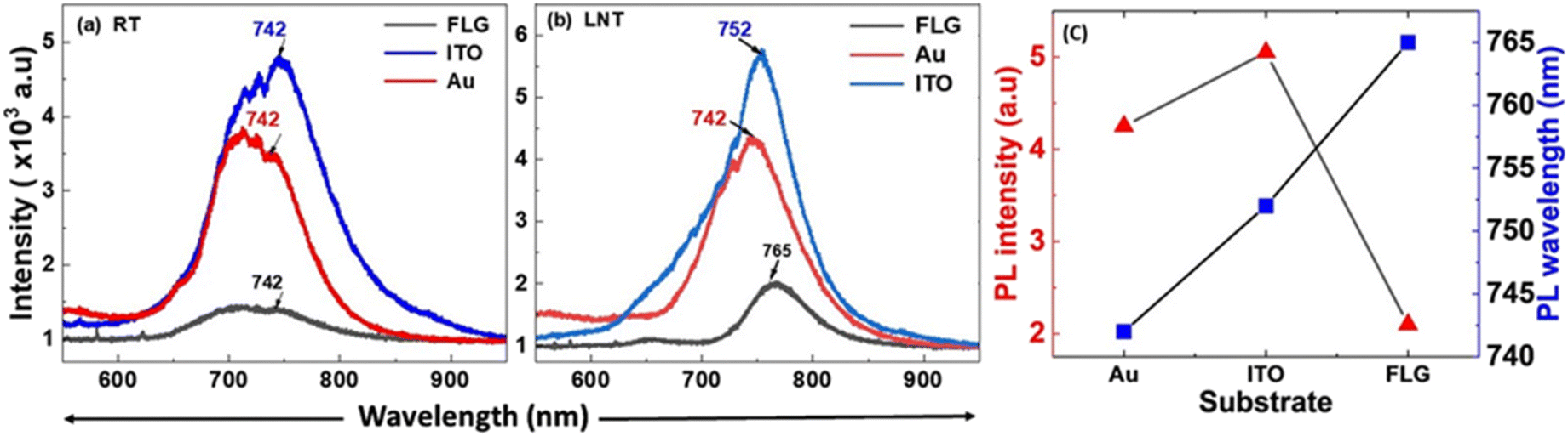 | ||
| Fig. 6 Comparison of PL spectra of p-MoS2 on substrates ITO (solid blue), Au (solid red) and FLG (solid black) at (a) RT and (b) LNT, illustrating a significant enhancement in PL emission on conductive substrates due to charge transfer from the substrates to p-MoS2, induced by work function differences between the substrates and p-MoS2. (c) PL peak intensity and PL peak wavelength distribution of monolayer p-MoS2 on three different substrates at LNT. | ||
However, at LNT, an enhanced, red-shifted PL peak is observed at 765 nm. This redshift observed at LNT is attributed to the same cause as that for the ITO substrate. However, the shift observed on FLG differs from that on ITO due to the difference in the work function between the two materials, as clearly shown in Fig. 6b (solid black). Therefore, ITO and Au substrates significantly enhance the PL emission of p-MoS2, far exceeding the emission observed on FLG at both RT and LNT, with comparable proportions of enhancement. Fig. 6c illustrates the variation in the PL intensity and wavelength in relation to different substrates at LNT. The temperature-dependent PL spectra of p-MoS2 are depicted in Fig. 7 for three different substrates, wherein the PL intensity increases monotonically with decreasing temperature on all substrates, which is attributed to a reduction in carrier scattering and suppression of non-radiative recombination processes. Similarly, the temperature-dependent PL spectra of n-MoSe2 are presented in Fig. S6 [ESI†]. Fig. 8 presents PL mapping images of monolayer p-MoS2 on various substrates. The images demonstrate consistent emission intensity and wavelength, indicating a uniform, high-quality monolayer flakes.
 | ||
| Fig. 7 Temperature-dependent PL spectra of p-MoS2 on (a) ITO, (b) Au and (c) FLG. As the temperature decreases from 0 °C to –175 °C, the PL intensity increases monotonically on all substrates, attributed to a reduction in carrier scattering and suppression of non-radiative recombination processes. | ||
 | ||
| Fig. 8 PL mapping images of monolayers of p-MoS2, obtained from the regions highlighted by red square boxes in the optical images, on (a) ITO, (b) Au and (c) FLG. The images illustrate consistent emission intensity and wavelength, indicating a uniform, high-quality monolayer flakes. | ||
The ratio of the spectral weights of A0 and A+ for different substrates can be extracted by deconvoluting the PL peaks. Fig. 8 presents the deconvoluted PL emission spectra of p-MoS2 on different substrates at LNT, providing insights into the spectral weight distribution between A0 and A+. It is evident that the spectral intensity ratio of A0 to A+ is higher on ITO compared to Au, confirming our earlier hypothesis that reversible charge transfer is more pronounced on ITO than on Au, resulting in enhanced PL emission on ITO compared to that on Au [Fig. 9a and b]. In contrast, in the FLG-passivated ITO substrate, the spectral weight of A+ exceeds that of A0, resulting in weaker PL emission [Fig. 9c]. The B peak, arising from band-to-band transitions, is better resolved in the FLG-passivated sample due to the complete suppression of substrate peaks. However, in the case of ITO and Au, the substrate peaks are not completely suppressed, which prevents the B peak from being resolved. This study clearly demonstrates that substrate choice plays a crucial role in modulating the PL emission properties of 2D TMDs and fabricating mono-layers of p-type TMDs on conducting substrates is an effective way to enhance their PL emission properties. This is due to the fact that the carrier concentration in p-type TMDCs is much larger than that in the n-type TMDs resulting in more number of charge transfers across the metal–semiconductor junction. Consequently, p-type MoS2 has more A0 than the n-type, thereby exhibiting strong PL emission, highlighting its importance in device optimization. This strong emission characteristic can be passed onto the n-type TMD if it is integrated with p-type TMD. The greater work function difference coupled with the higher gradient in the carrier concentration will drive more charge carriers across the p–n bilayers leading to a greater increase in A0 excitons.
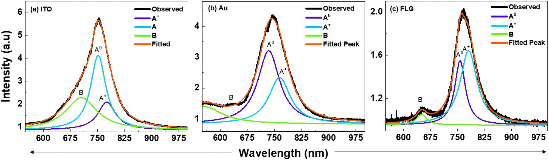 | ||
| Fig. 9 Deconvoluted PL spectra of monolayers of p-MoS2 at LNT on substrates (a) ITO, (b) Au and (c) FLG illustrating the spectral weight distribution of charged excitons (A+) and neutral excitons (A0). The Solid black line represents the observed PL peak, while the solid red line is the fit to the Lorentzian peaks (A+, A0, and B). | ||
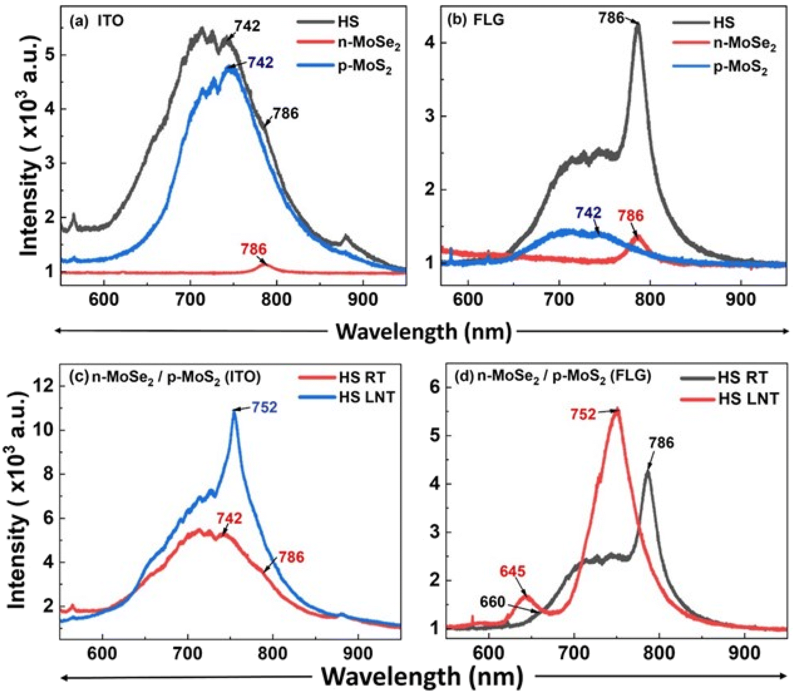
Therefore, a hetero-bilayer comprising monolayers of p-MoS2 and n-MoSe2 was fabricated on ITO and FLG-passivated ITO substrates with the objective of increasing the PL intensity [Fig. 10a and b]. The presence of both the monolayers is confirmed by Raman spectra [Fig. 10c]. n-MoSe2 was chosen instead of n-MoS2 because the lower work function of n-MoSe2 ensures a larger carrier injection from n-MoSe2 to p-MoS2. Also, it is observed that the PL peak of n-MoSe2 blue shifts to 752 nm from 785 nm at LNT [Fig. 11], which brings an advantage to enhance PL emission at HJ significantly, as PL emission of p-MoS2 is found to be at 752 nm at LNT. At the HJ, the PL spectra displayed enhanced peaks for both p-MoS2 and n-MoSe2 compared to those from free-standing monolayers, on both the substrates [Fig. 12a and b]. This enhancement is attributed to the charge transfer within the HJ and across the heterostructure–substrate interface, driven by the differential work functions of the materials. Charge transfer occurs from MoSe2 and ITO to MoS2. In contrast, in the FLG-passivated ITO substrate, charge transfer occurs only from MoSe2 to MoS2. It is to be noted that in n-MoSe2, the presence of excess electrons will favour the formation of negative trions (A−) compared to A0 on an insulating substrate.
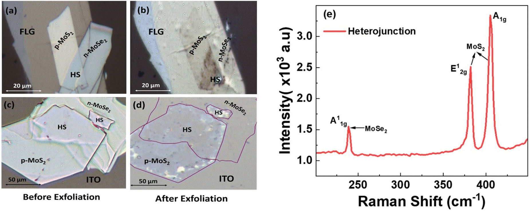 | ||
| Fig. 10 Optical images of the heterostructures of p-MoS2 and n-MoSe2 before and after photo-exfoliation on (a and b) FLG and (c and d) ITO. (e) Raman spectra of the heterostructure depicting the corresponding Raman peaks of p-MoS2 and n-MoSe2. | ||
 | ||
| Fig. 11 PL spectra of monolayers of n-MoSe2 at RT and LNT on substrates (a) ITO and (b) FLG. AT LNT, the PL peak shifts from 786 nm to 752 nm on both substrates compared to the RT measurements. | ||
 | ||
| Fig. 12 Comparison plots illustrating the enhancement of PL emission in the heterostructure relative to free-standing monolayers on (a) ITO and (b) FLG. Comparison plots illustrating enhancement of PL emission in the heterostructure at LNT compared to RT on (c) ITO and (d) FLG. | ||
An enhancement of 192% in the PL emission of MoSe2 was observed compared to the PL peaks of free-standing MoSe2 monolayers on the FLG substrate. This significant increase is attributed to the charge transfer from MoSe2 to MoS2 and to the FLG substrate, which reduces the concentration of A− (by increasing the A0 concentration) in MoSe2. However, a 118% increase in PL emission was observed on the ITO substrate, where charge transfer was limited to interactions between n-MoSe2 and p-MoS2. For p-MoS2, an 85% increase in the PL intensity was observed on the FLG substrate, facilitated by charge transfer due to the differential work function of the materials, and a 17% increase in the PL intensity was noted on the ITO substrate.
At liquid nitrogen temperature (LNT), highly enhanced PL emission at 752 nm was recorded for both the heterostructures, attributed to a blue shift of 33 nm in the PL peak of n-MoSe2, from 785 nm (RT) to 752 nm (LNT), and a red shift of 10 nm in the A peak of p-MoS2, from 742 nm (RT) to 752 nm (LNT). The convergence of these peaks at the same emission energy of 1.64 eV at LNT results in a single, strong, and resonant emission peak. The blue shift in n-MoSe2 is due to the increase in the bandgap at low temperatures, consistent with previous studies.29 In p-MoS2, the red shift is caused by the coupling of free electrons with neutral excitons, leading to the formation of A− with lower recombination energy. LNT measurements of the heterostructure reveal a significant enhancement in PL emission, attributed to increased radiative recombinations [Fig. 12c and d]. This unique behavior, characterized by a resonant strong PL emission (A-peak) at the heterojunction on both substrates underscores the significant advantage in enhancing PL emission in p–n hetero-bilayers of TMDs. These findings indicate that p-type 2D TMDs hold substantial potential for optoelectronic applications. When integrated with other 2D TMDs, they could offer considerable advantages for practical nano-electronic device applications.
Conclusion
In this study, we demonstrated reverse charge injection-induced enhancement of excitonic emission in photo-exfoliated monolayers of p-MoS2, attributed to the differential work function between p-MoS2 and substrates. ITO and Au serve as source charge injectors to p-MoS2, enhancing its PL emission, while FLG acts as a barrier layer between ITO and p-MoS2, preventing charge transfer and leading to a sharp decrease in PL emission. The PL emission of p-MoS2 is further amplified at low temperatures, owing to increased radiative recombinations. To capitalize on the enhanced PL emission of p-MoS2, we fabricated a hetero-bilayer on substrates (ITO and FLG) using the photo-exfoliation technique, consisting of monolayers of p-MoS2 and n-MoSe2. At the HJ, PL emission in both p-MoS2 and n-MoSe2 was significantly enhanced compared to free-standing monolayers on both the substrates. When cooled to LNT, a single, resonant, and highly intense PL peak was observed at the HJ at 1.64 eV, resulting from a blue shift of the n-MoSe2 peak and a red shift of the p-MoS2 peak. This enhanced PL emission, observed from both p-MoS2 and n-MoSe2 at the same energy at the HJ, along with the increased PL emission in p-MoS2 on low work-function substrates, provides valuable insights into the role of stacking 2D-TMDs and substrate selection. This understanding is crucial for advancing the development of next-generation optoelectronic devices.Author contributions
Rashed H. Lone: experimental conceptualization, investigation, device fabrication, data curation, formal analysis, and writing – original draft, and writing – review and editing. Shreya Gaonkar: investigation, performing experiments, formal analysis, data curation, device fabrication and writing – original draft, and writing – review and editing. B. Manoj Kumar: performing experiments and data curation. E. S. Kannan: funding acquisition, validation and supervision.Data availability
The data that support the findings of this study are available from the corresponding author upon reasonable request.Conflicts of interest
The authors have no conflicts to disclose.Acknowledgements
The work was supported by the CDRF grant instituted by BITS-Pilani University. The authors would like to thank the Central Sophisticated Instrumental Facility (CSIF) at BITS-Pilani K. K. Birla Goa Campus for providing access to the experimental facility. The authors would also like to thank C Malavika from TIFR Hyderabad for providing the AFM measurements.References
- K. S. Novoselov, A. K. Geim, S. V. Morozov, D. Jiang, Y. Zhang, S. V. Dubonos, I. V. Grigorieva and A. A. Firsov, Science, 2004, 306, 666–669 CrossRef CAS PubMed.
- M. Chhowalla, H. S. Shin, G. Eda, L.-J. Li, K. P. Loh and H. Zhang, Nat. Chem., 2013, 5, 263–275 CrossRef PubMed.
- D. Xiao, G.-B. Liu, W. Feng, X. Xu and W. Yao, Phys. Rev. Lett., 2012, 108, 196802 CrossRef PubMed.
- K. F. Mak, C. Lee, J. Hone, J. Shan and T. F. Heinz, Phys. Rev. Lett., 2010, 105, 136805 CrossRef PubMed.
- R. S. Sundaram, M. Engel, A. Lombardo, R. Krupke, A. C. Ferrari, P. Avouris and M. Steiner, Nano Lett., 2013, 13, 1416–1421 CrossRef CAS PubMed.
- Q. H. Wang, K. Kalantar-zadeh, A. Kis, J. Coleman and M. Strano, Nat. Nanotechnol., 2012, 7, 699–712 CrossRef CAS PubMed.
- H. Nan, Z. Wang, W. Wang, Z. Liang, Y. Lu, Q. Chen, D. He, P. Tan, F. Miao, X. Wang, J. Wang and Z. Ni, ACS Nano, 2014, 8, 5738–5745 CrossRef CAS PubMed.
- S. V. Sivaram, A. T. Hanbicki, M. R. Rosenberger, G. G. Jernigan, H.-J. Chuang, K. M. McCreary and B. T. Jonker, ACS Appl. Mater. Interfaces, 2019, 11, 16147–16155 CrossRef CAS PubMed.
- H. Ardekani, R. Younts, Y. Yu, L. Cao and K. Gundogdu, ACS Appl. Mater. Interfaces, 2019, 11, 38240–38246 CrossRef CAS PubMed.
- L. Fang, L. Su, H. Guan, Z. Liu, Y. Yu, D. Cao, X. Chen and H. Shu, ACS Appl. Nano Mater., 2024, 7, 5063–5073 CrossRef CAS.
- S. Tongay, J. Suh, C. Ataca, W. Fan, A. Luce, J. S. Kang, J. Liu, C. Ko, R. Raghunathanan, J. Zhou, F. Ogletree, J. Li, J. C. Grossman and J. Wu, Sci. Rep., 2013, 3, 2657 CrossRef PubMed.
- W. Wang, H. Shu, J. Wang, Y. Cheng, P. Liang and X. Chen, ACS Appl. Mater. Interfaces, 2020, 12, 9563–9571 CrossRef CAS PubMed.
- Z. Lin, B. R. Carvalho, E. Kahn, R. Lv, R. Rao, H. Terrones, M. A. Pimenta and M. Terrones, 2D Mater., 2016, 3, 022002 CrossRef.
- W. Li, M. Xin, W. Lan, Q. Bai, S. Du, G. Wang, B. Liu and C. Gu, Laser Photonics Rev., 2022, 16, 2200008 CrossRef CAS.
- I. Irfan, S. Golovynskyi, M. Bosi, L. Seravalli, O. A. Yeshchenko, B. Xue, D. Dong, Y. Lin, R. Qiu, B. Li and J. Qu, J. Phys. Chem. C, 2021, 125, 4119–4132 CrossRef CAS.
- R. Pan, J. Kang, Y. Li, Z. Zhang, R. Li and Y. Yang, ACS Appl. Mater. Interfaces, 2022, 14, 12495–12503 CrossRef CAS PubMed.
- H.-J. Kim, Y. J. Yun, S. N. Yi, S. K. Chang and D. H. Ha, ACS Omega, 2020, 5, 7903–7909 CrossRef CAS PubMed.
- H. Y. Lee, M. M. Al Ezzi, N. Raghuvanshi, J. Y. Chung, K. Watanabe, T. Taniguchi, S. Garaj, S. Adam and S. Gradečak, Nano Lett., 2021, 21, 2832–2839 CrossRef CAS PubMed.
- Y. Liu, C. Zeng, J. Yu, J. Zhong, B. Li, Z. Zhang, Z. Liu, Z. M. Wang, A. Pan and X. Duan, Chem. Soc. Rev., 2021, 50, 6401–6422 RSC.
- H. Zheng, B. Wu, S. Li, J. Ding, J. He, Z. Liu, C.-T. Wang, J.-T. Wang, A. Pan and Y. Liu, Light: Sci. Appl., 2023, 12, 117 CrossRef CAS PubMed.
- H. Fang, C. Battaglia, C. Carraro, S. Nemsak, B. Ozdol, J. S. Kang, H. A. Bechtel, S. B. Desai, F. Kronast, A. A. Unal, G. Conti, C. Conlon, G. K. Palsson, M. C. Martin, A. M. Minor, C. S. Fadley, E. Yablonovitch, R. Maboudian and A. Javey, Proc. Natl. Acad. Sci. U. S. A., 2014, 111, 6198–6202 CrossRef CAS PubMed.
- X. Hong, J. Kim, S.-F. Shi, Y. Zhang, C. Jin, Y. Sun, S. Tongay, J. Wu, Y. Zhang and F. Wang, Nat. Nanotechnol., 2014, 9, 682–686 CrossRef CAS PubMed.
- S. Luo, X. Qi, J. Li, L. Ren, G. Guo, Q. Peng, J. Li and J. Zhong, J. Phys. Chem. Solids, 2019, 128, 337–342 CrossRef CAS.
- J. Yuan, S. Najmaei, Z. Zhang, J. Zhang, S. Lei, P. M. Ajayan, B. I. Yakobson and J. Lou, ACS Nano, 2015, 9, 555–563 CrossRef CAS PubMed.
- M. Ramos, F. Marques-Moros, D. L. Esteras, S. Mañas-Valero, E. Henríquez-Guerra, M. Gadea, J. J. Baldoví, J. Canet-Ferrer, E. Coronado and M. R. Calvo, ACS Appl. Mater. Interfaces, 2022, 14, 33482–33490 CrossRef CAS PubMed.
- Y. Hwang, T. Kim and N. Shin, ACS Appl. Nano Mater., 2021, 4, 12034–12042 CrossRef CAS.
- V. Carozo, K. Fujisawa, R. Rao, E. Kahn, J. R. Cunha, T. Zhang, D. Rubin, M. F. Salazar, A. De Luna Bugallo, S. Kar and M. Terrones, 2D Mater., 2018, 5, 031016 CrossRef.
- J. Duan, P. Chava, M. Ghorbani-Asl, D. Erb, L. Hu, A. V. Krasheninnikov, H. Schneider, L. Rebohle, A. Erbe, M. Helm, Y.-J. Zeng, S. Zhou and S. Prucnal, Adv. Funct. Mater., 2021, 31, 2104960 CrossRef CAS.
- B. Wu, H. Zheng, S. Li, J. Ding, J. He, Z. Liu and Y. Liu, Nano Res., 2022, 15, 5640–5645 CrossRef CAS.
- X. Wang, Y. Zhao, X. Kong, Q. Zhang, H. K. Ng, S. X. Lim, Y. Zheng, X. Wu, K. Watanabe, Q.-H. Xu, T. Taniguchi, G. Eda, K. E. J. Goh, S. Jin, K. P. Loh, F. Ding, W. Sun and C. H. Sow, ACS Nano, 2022, 16, 8172–8180 CrossRef CAS PubMed.
- M. Gao, L. Yu, Q. Lv, F. Kang, Z.-H. Huang and R. Lv, J. Materiomics, 2023, 9, 768–786 CrossRef.
- J. Suh, T. L. Tan, W. Zhao, J. Park, D.-Y. Lin, T.-E. Park, J. Kim, C. Jin, N. Saigal, S. Ghosh, Z. M. Wong, Y. Chen, F. Wang, W. Walukiewicz, G. Eda and J. Wu, Nat. Commun., 2018, 9, 199 CrossRef PubMed.
- H. Fang, S. Chuang, T. C. Chang, K. Takei, T. Takahashi and A. Javey, Nano Lett., 2012, 12, 3788–3792 CrossRef CAS PubMed.
- S. Wang, W. Zhao, F. Giustiniano and G. Eda, Phys. Chem. Chem. Phys., 2016, 18, 4304–4309 RSC.
- C. Malavika, B. Manoj Kumar and E. S. Kannan, Appl. Phys. Lett., 2022, 120, 143503 CrossRef CAS.
- C. Lee, H. Yan, L. E. Brus, T. F. Heinz, J. Hone and S. Ryu, ACS Nano, 2010, 4, 2695–2700 CrossRef CAS PubMed.
- H. Li, Q. Zhang, C. C. R. Yap, B. K. Tay, T. H. T. Edwin, A. Olivier and D. Baillargeat, Adv. Funct. Mater., 2012, 22, 1385–1390 CrossRef CAS.
- Y. Wang, C. Cong, C. Qiu and T. Yu, Small, 2013, 9, 2857–2861 CrossRef CAS PubMed.
- A. Splendiani, L. Sun, Y. Zhang, T. Li, J. Kim, C.-Y. Chim, G. Galli and F. Wang, Nano Lett., 2010, 10, 1271–1275 CrossRef CAS PubMed.
- H. Li and X. H. Zhang, Opt. Mater., 2020, 107, 110150 CrossRef CAS.
- J. W. Christopher, B. B. Goldberg and A. K. Swan, Sci. Rep., 2017, 7, 14062 CrossRef PubMed.
Footnotes |
| † Electronic supplementary information (ESI) available. See DOI: https://doi.org/10.1039/d4nr04009k |
| ‡ These authors contributed equally to this work. |
| This journal is © The Royal Society of Chemistry 2025 |