
 Open Access Article
 This Open Access Article is licensed under a Creative Commons Attribution-Non Commercial 3.0 Unported Licence
Self-patterning of liquid Field's metal for enhanced performance of two-dimensional semiconductors†
Kwanghee Han‡
 ab,
Heeyeon Lee‡a,
Minseong Kwonac,
Vinod Menonb,
Chaun Jangc and
Young Duck Kim*ad
ab,
Heeyeon Lee‡a,
Minseong Kwonac,
Vinod Menonb,
Chaun Jangc and
Young Duck Kim*ad
aDepartment of Physics, Kyung Hee University, Seoul, 02447, Republic of Korea. E-mail: ydk@khu.ac.kr
bDepartment of Physics, City College of New York, New York, NY 10031, USA
cCenter for Spintronics, Korea Institute of Science and Technology, Seoul, 02792, Republic of Korea
dDepartment of Information Display, Kyung Hee University, Seoul, 02447, Republic of Korea
First published on 27th May 2025
Abstract
Two-dimensional (2D) van der Waals semiconductors show promise for atomically thin, flexible, and transparent optoelectronic devices in future technologies. However, developing high-performance field-effect transistors (FETs) based on 2D materials is impeded by two key challenges, namely, the high contact resistance at the 2D semiconductor–metal interface and limited effective doping strategies. Here, we present a novel approach to overcome these challenges using self-propagating liquid Field's metal, a eutectic alloy with a low melting point of approximately 62 °C. By modifying pre-patterned electrodes on WSe2 FETs through the deposition of Field's metal onto contact pad edges followed by vacuum annealing, we create new semimetal electrodes that seamlessly incorporate the liquid metal into 2D semiconductors. This integration preserves the original electrode architecture while transforming to semimetal compositions of Field's metal, such as Bi, In, and Sn, modifies the work functions to 2D semiconductors, resulting in reduced contact resistance without inducing Fermi-level pinning, and improves charge carrier mobilities. Our method enhances the electrical performance of 2D devices and opens new avenues for designing high-resolution liquid metal circuits suitable for stretchable, flexible, and wearable 2D semiconductor applications.
1. Introduction
One of the breakthroughs for future electrical devices is developing integrated circuits based on the 2-dimensional (2D) semiconductor. However, creating a reliable contact between the metal electrodes and 2D transition metal dichalcogenides (TMD) has been challenging. Due to metal-induced gap states (MIGS),1–5 Schottky barriers lead to increased contact resistance and reduced on-current density.6,7 Meanwhile, recent work has demonstrated breakthroughs for low contact resistance in 2D TMD devices using bismuth (Bi),8 indium (In),9 and their alloys as electrodes.10,11 Here, we propose a new strategy to reduce the contact resistance of 2D semiconductors by using self-propagation of Field's metal. Previously, Field's metal has been used to make ohmic contact with graphene devices using the micro-soldering method.12 In addition, it has been used to investigate van Hove singularities in the local density of states for magic-angle-twisted bilayer graphene.13 This work demonstrated extremely precise electrodes using liquid Field's metals on pre-patterned structures. Since the Field's metal alloy contains Bi, In, and Sn,14,15 our strategy can be utilized to enhance the performance of 2D semiconductor-based electronics.2. Results
2.1. Self-propagation of liquid Field's metal by vacuum annealing
Metals or conductors that become liquid near room temperature offer several advantages. First, they can be utilized in stretchable, soft electrical devices,16 which have great potential for clothing, medical implants, or wearable materials for key applications.17 Second, liquid-metal patterning is a significantly simpler process compared to physical vapor deposition (PVD) techniques, which require high temperatures and vacuum conditions to melt metals (T > 1000 °C).18 Finally, liquid metals are highly reconfigurable, allowing precise control of their shape and position once heated to their melting point (T < 100 °C).19–23 Consequently, various approaches have been developed to print liquid metal circuits, including techniques such as direct writing24,25 and the voltage-induced self-healing effect.26Despite the great potential of liquid metal for flexible electronic applications, conventional fabrication methods for liquid metal electrodes face several challenges. Liquid metal electrode fabrication methods are constrained by limited fabrication resolution,18 with reported resolutions of ∼2 μm for imprint techniques,19 ∼10 μm for injection methods,18 and ∼100 μm for direct wire methods.25,27 Another challenge is reduced electrical contact with semiconductors due to formation of native oxide layers. For instance, liquid gallium forms a gallium oxide layer when exposed to ambient conditions,28 and such native oxide layers make it more difficult to use liquid metals in fabricating semiconductor devices with low-contact resistance.18
Recent studies have shown that precise liquid metal electrodes can be made using intermetallic bond-assisted patterning.29–32 Since liquid metal alloys are mixed with other metals, the liquid metal can be deposited on the pre-patterned substrate and spread by jetting or rolling. In addition, etching solutions are used to remove surface oxide and liquid metal residues, resulting in liquid metal electrodes with resolution larger than 50 μm.32 A further issue is the use of mechanical force to remove metal alloys from the mold and placing the assembly in chemical solutions for cleaning, which could damage the patterned electrodes. In our work, however, self-propagation of the liquid metal along the pre-patterned electrodes does not require any mechanical or chemical post-processing, and our method offers significantly higher resolution (∼200 nm) than conventional liquid metal fabrication techniques.
Self-propagation is a new physical property of liquid metals which can facilitate formation of new alloys with metal surfaces via heating. It is a different technique from other methods used in previous research such as rolling29 and applying voltage.23,33 Furthermore, unlike these previous techniques, self-propagation occurs even under ambient pressure conditions, indicating that the processing of the Field's metal is driven by intrinsic material properties rather than external pressure differences (ESI Note 3†).
As shown in Fig. 1a, the liquid Field's metal self-propagates along the pre-patterned electrodes during vacuum annealing above the melting point (T > 62 °C) and accurately forms the semimetal electrode composite (including Bi, In, and Sn) with the same shape as the original pre-patterned electrodes (Au/Cr). To investigate this process, we prepared pre-patterned electrodes separated by two electrode gaps of 0.2–5 μm distance (Fig. 1b and c). After vacuum thermal annealing (T ∼ 300 °C, 2 h), we observed the self-propagation of liquid Field's metal through the pre-patterned electrodes without significant spread of the metal through the SiO2 substrate and it's hopping of the 200 nm gap as shown in the optical images (Fig. 1d and e) and the scanning electron microscopy (SEM) images (Fig. 1f and g). Thus, our electrode formation techniques using self-propagating liquid Field's metal show a higher resolution than conventional methods when fabricating precise nanoscale liquid metal electrodes.18,19,25,27 According to resolution tests for this method, we could realize Field's metal electrodes with ∼200 nm width (ESI Note 4†). In addition, the accuracy of self-patterned liquid Field's metal electrodes is the same as the resolution of electrodes obtained from e-beam lithography.
 | ||
| Fig. 1 Self-propagation of Field's metal by vacuum annealing. (a) Schematic diagram of the self-propagation effect of liquid metal. (b and c) Optical images of pre-patterned Au/Cr electrodes after placing Field's metal on top of the surface. (d and e) Optical images after vacuum annealing. The Field's metal propagated through the electrodes. (f and g) SEM images of Field's metal electrodes. Accurate electrodes with dimensions of a few hundred nanometers can be produced by this method. | ||
By applying the self-propagation liquid metal technique, devices that feature 2D semiconductor FETs can be readily fabricated with Field's metal electrodes. Fig. 2a is a schematic illustration of a multilayer WSe2 device assembled via the self-propagation of liquid Field's metal. After placing Field's metal on the edge of each gold electrode and subjecting it to vacuum annealing, the electrodes can be reformed with the same design as pre-patterned electrodes using the semimetal alloys of the Field's metal. To determine the contact resistance value of the WSe2 device, we use the transfer-length method (TLM). The pre-patterned Cr/Au electrodes are fabricated using multilayer WSe2 flake (61 nm) with different values of channel length (LCH = 1 μm, 2 μm, 3 μm, 4 μm) but having the same metal contact length (Lc) of 1 μm. All channels have width (W) values of 7 μm. As shown in the optical images of Fig. 2b and c, we can confirm that Field's metal electrodes successfully reform after self-propagation under vacuum annealing.
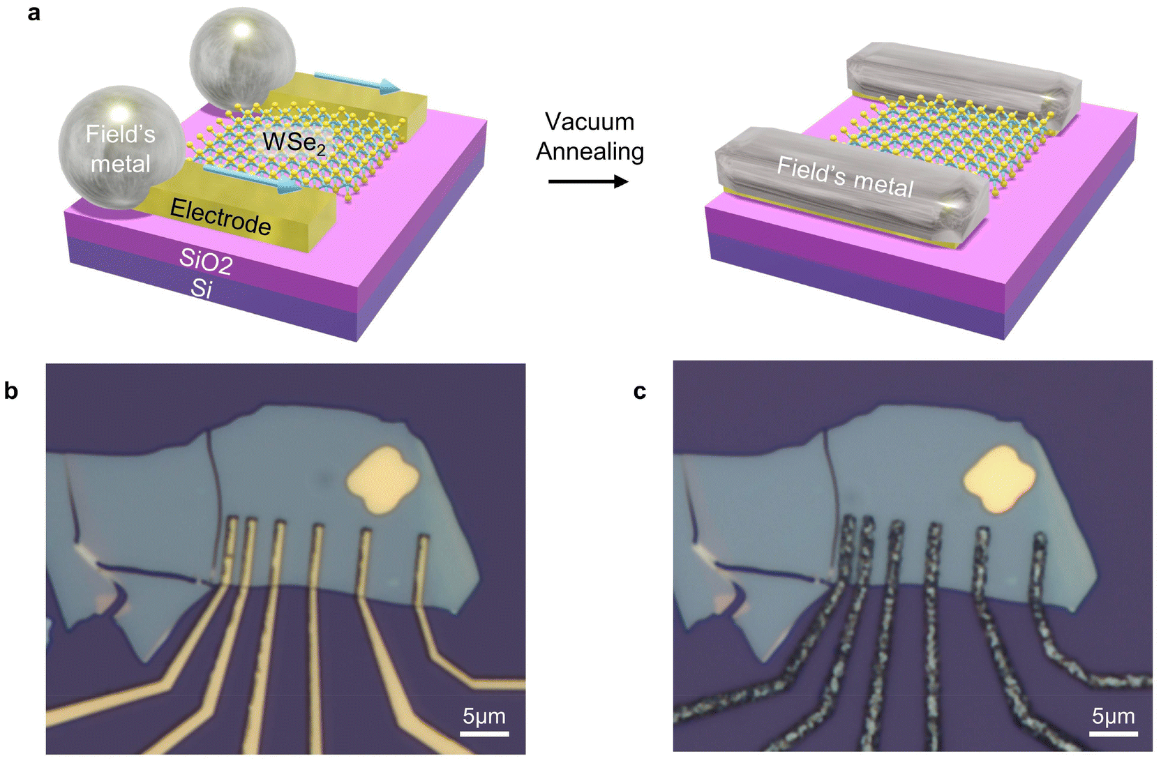 | ||
| Fig. 2 A WSe2 FET device with Field's metal electrodes obtained using self-propagation. (a) Schematic illustration of the assembly of a WSe2 field-effect transistor by using the self-propagation method. (b) Optical image of the device before annealing. (c) Optical image of the device after annealing. The Field's metal was formed accurately with the same structure as the Au/Cr electrodes. | ||
2.2. Electrical properties of a WSe2 FET device with Field's metal electrodes
To compare the pre-patterned (Au/Cr) and liquid Field's metal alloy composite (Bi/In/Sn) electrical contacts with the WSe2, we measured their transfer characteristics (IDS–VG) under constant VSD = 1 V at room temperature. As shown in Fig. 3a, the on-current at a high gate voltage (VG = 60 V) increased from 1.18 μA to 6.12 μA (∼5.2 times) after forming the Field's metal electrodes. Furthermore, the output characteristics (IDS–VDS) show a significant increase in current flow up to ∼14.6 times under a lower gate voltage (VG = 40 V) and higher saturation currents after the self-propagation process, as shown in Fig. 3d and e. This is attributed to the reformation of pre-patterned electrodes by liquid Field's semimetal alloy composites (Bi, In, Sn), significantly lowering the contact resistance between 2D semiconductors and metal electrodes. | ||
| Fig. 3 Comparison between electrical characteristics of contact of Au/Cr and Field's metal electrodes with WSe2. (a) Room-temperature transfer characteristics (IDS–VG) before and after self-propagation of Field's metal. The on-current is increased by ∼5.2 times after the process. (b) The band structures of metal–semiconductor contact showing a Schottky barrier by metal-induced gap states (MIGS). (c) The band structures of semimetal–semiconductor interaction that exhibits ohmic contact by preventing gap-state pinning. (d and e) Output characteristics (IDS–VDS) at room temperature of the WSe2 FET device before and after forming Field's metal electrodes. | ||
Au/Cr is a common material used to make electrodes in 2D material-based devices, but its Schottky barrier results in high contact resistance. For instance, a recent report indicated that WSe2 with Cr contacts exhibits a mobility of 1.838 cm2 V−1 s−1 and a contact resistance of 496 kΩ μm−1.34 Also, Cr (∼4.5 eV) and Au (∼5.1 eV) do not align well with the valence band of WSe2 (∼5.3–5.4 eV), resulting in a large Schottky barrier for p-type injection.35 Furthermore, chromium can chemically react with the WSe2 surface, potentially forming defects at the interface, which may degrade device performance.36,37 However, our results show that the n-type contact can be improved by this method. Although achieving good n-type contact with WSe2 is challenging, our results demonstrate a clear improvement in contact performance.
Fig. 3b shows the band structure of the contact between metal and semiconductor, which explains the high contact resistance with gold electrodes and WSe2. Because of the energy difference between metal and semiconductor and MIGS via Fermi-level pinning, the Schottky barrier is created and this results in higher contact resistance.7 However, as Fig. 3c reveals, the contact resistance is reduced by using semimetal materials as electrodes. Because the semimetal, bismuth and indium, can facilitate ohmic contact with TMDC,8,9 the Field's metal electrodes can lower the Schottky barrier height with the same mechanism. The self-propagation of liquid Field's metal enables the modification of the work function of pre-patterned metal electrodes through the formation of semi-metallic alloys, demonstrating its potential for tuning band alignment to enhance the electrical performance of 2D semiconductor devices.
As shown in Fig. 4, we also estimated the field-effect mobility (μFE) of each channel and the contact resistance (RC) from the transfer characteristics (IDS–VG). The log-scale transfer characteristics by channel length show a significant difference in the electrical properties before (Fig. 4a) and after (Fig. 4b) self-propagation of the liquid Field's metal contact. Fig. 4c shows the relationship between the threshold voltage and the channel length of the WSe2 FET device. The threshold voltages of the fabricated WSe2 FET channels are initially around Vth = 0 V, but there is a significant negative shift of threshold voltage after the transformation of the Field's metal electrodes. This is attributed to the formation of transparent contacts with semimetal alloys and the reduction of Fermi-level pinning caused by metal-induced gap states.
 | ||
| Fig. 4 Contact resistance reduced by self-propagation of Field's metal. (a and b) Log-scale transfer characteristics (IDS–VG) as a function of the channel length (a) before and (b) after self-propagation. (c) Threshold voltage (Vth) by channel length is changed after forming the Field's metal electrode. (d) Comparison of electron mobilities from the WSe2 FET device before and after fabricating the Field's metal contact. (e) Contact resistance (RC) measured by using the transfer-length method (TLM). | ||
Fig. 4d shows that the mobility is increased by the Field's metal contact. The field effect mobilities are calculated by using the equation,  , where W is the channel width, L is the channel length, and Ci is the capacitance between the channel and back gate per unit area. Before forming the Field's metal electrodes, the electron mobility values, indicated by blue dots, range from ∼0.7684 cm2 V−1 s−1 (LCH = 1 μm) to ∼3.2814 cm2 V−1 s−1 (LCH = 4 μm). On the other hand, after the transformation process with self-propagation of liquid Field's metal, the mobility values are increased, as shown by the red dots in Fig. 4d, from ∼1.1602 cm2 V−1 s−1 (LCH = 1 μm) to ∼5.969 cm2 V−1 s−1 (LCH = 4 μm). By comparing these results, μFE has increased by about 1.51–1.82 times after formation of the Field's metal contact.
To investigate the reduction in contact resistance (Rc) by using liquid Field's metal, we measured the two-probe resistance (RT) as follows:8,38
| RT = 2Rc + Rch = 2Rc + RshLch |
3. Conclusion
In summary, we demonstrate the realization of high-resolution self-patterned liquid Field's metal to achieve transparent contact with 2D semiconductor devices. Simply placing the Field's metal on the pre-patterned electrodes and applying vacuum annealing enhances the electrical performance, as evidenced by increased mobility and reduced contact resistance. This occurs due to the transformation of Cr/Au electrodes into a semimetal alloy of Bi, In, and Sn, which reduces the Fermi level pinning effect caused by metal-induced gap states (MIGS) in WSe2.8 Additionally, liquid metals composed of materials with varying work functions can be utilized, enabling more efficient interfacial charge transfer and lower contact resistance in 2D semiconductor FETs.9 Since this technique facilitates the fabrication of high-resolution liquid metal electrodes, it paves the way to developing nano-scale liquid metal electrodes for stretchable, flexible, and highly reconfigurable 2D integrated circuits.4. Methods
4.1. Sample preparation
WSe2 flakes were mechanically exfoliated onto 285 nm-thick SiO2 using the Scotch tape technique. Pre-patterned electrical contacts were defined using electron-beam lithography (Zeiss Sigma 300 with NPGS) conducted at the Multidimensional Materials Research Center at Kyung Hee University (2021R1A6C101A437). PMMA A6 was used as the e-beam resist after spin coating at 2000 rpm for 60 s. It was baked at 180 °C for 5 min. After e-beam lithography, the samples were developed under IPA![[thin space (1/6-em)]](https://www.rsc.org/images/entities/char_2009.gif) :DI water = 3:1 for 1 min. All the electrodes were deposited using a thermal evaporator (3 nm Cr, 60 nm Au). After deposition, we placed the samples in acetone overnight for the lift-off process. To make the Field's metal electrodes, we positioned a piece of Field's metal on the electrodes and annealed it under vacuum (200–300 °C, ∼10−6 Torr) for 2 hours.
:DI water = 3:1 for 1 min. All the electrodes were deposited using a thermal evaporator (3 nm Cr, 60 nm Au). After deposition, we placed the samples in acetone overnight for the lift-off process. To make the Field's metal electrodes, we positioned a piece of Field's metal on the electrodes and annealed it under vacuum (200–300 °C, ∼10−6 Torr) for 2 hours.
4.2. Device characterization
All electrical measurements were conducted under vacuum (∼10−6 Torr) on a probe station (MS TECH) using a parameter analyzer (HP 4155A Semiconductor Parameter Analyzer). The thickness of the WSe2 samples was determined using AFM (Park Systems XE-100, Bruker Multimode 8). SEM images were obtained with a field emission scanning electron microscope (Zeiss Sigma 300, FEI Helios Nanolab 660).Author contributions
K. H. and Y. D. K. designed the research project and supervised the experiment. K. H. fabricated the Field's metal samples. K. H. and H. L. performed the electrical measurements. K. H. and H. L. obtained the SEM images. M. K. and K. H. used an e-beam evaporator for making the Au/Cr electrodes. The fabrication process was supervised by C. J. and V. M. K. H. and Y. D. K. analysed the data and wrote the paper. All authors contributed to the scientific planning and discussions and commented on the manuscript.Data availability
The data that support the findings of this study are available from the authors upon reasonable request.Conflicts of interest
There are no conflicts to declare.Acknowledgements
This research was supported by the National Research Foundation of Korea (NRF) grant funded by the Korea government (MSIT) (2021R1A2C2093155, 2021M3H4A1A03054856, 2022M3H4A1A04096396, RS-2023-00254055). This work was supported by a grant from Kyung Hee University in 2019 (KHU-20192441). K. H. was supported by Creation of the Quantum Information Science R&D Ecosystem (2022M3H3A1063074) through NRF Funded by MSIT. K.H., H. L. were supported by the MSIT under the ITRC (Information Technology Research Center) support program (IITP-2024-2710007945) supervised by the IITP (Institute for Information & Communications Technology Planning & Evaluation).References
- S. G. Louie and M. L. Cohen, Electronic structure of a metal-semiconductor interface, Phys. Rev. B, 1976, 13, 2461–2469 CrossRef CAS.
- T. Nishimura, K. Kita and A. Toriumi, Evidence for strong Fermi-level pinning due to metal-induced gap states at metal/germanium interface, Appl. Phys. Lett., 2007, 91, 123123 CrossRef.
- M. Kobayashi, A. Kinoshita, K. Saraswat, H.-S. P. Wong and Y. Nishi, Fermi level depinning in metal/Ge Schottky junction for metal source/drain Ge metal-oxide-semiconductor field-effect-transistor application, J. Appl. Phys., 2009, 105, 023702 CrossRef.
- K. Sotthewes, et al., Universal Fermi-Level Pinning in Transition-Metal Dichalcogenides, J. Phys. Chem. C, 2019, 123, 5411–5420 CrossRef CAS PubMed.
- C. Kim, et al., Fermi Level Pinning at Electrical Metal Contacts of Monolayer Molybdenum Dichalcogenides, ACS Nano, 2017, 11, 1588–1596 CrossRef CAS PubMed.
- A. Allain, J. Kang, K. Banerjee and A. Kis, Electrical contacts to two-dimensional semiconductors, Nat. Mater., 2015, 14, 1195–1205 CrossRef CAS.
- R. T. Tung, The physics and chemistry of the Schottky barrier height, Appl. Phys. Rev., 2014, 1, 011304 Search PubMed.
- P.-C. Shen, et al., Ultralow contact resistance between semimetal and monolayer semiconductors, Nature, 2021, 593, 211–217 CrossRef CAS PubMed.
- B.-K. Kim, et al., Origins of genuine Ohmic van der Waals contact between indium and MoS2, npj 2D Mater. Appl., 2021, 5, 1–10 CrossRef.
- C. S. Lau, et al., Quantum Transport in Two-Dimensional WS2 with High-Efficiency Carrier Injection through Indium Alloy Contacts, ACS Nano, 2020, 14, 13700–13708 CrossRef CAS PubMed.
- Y. Wang, et al., van der Waals contacts between three-dimensional metals and two-dimensional semiconductors, Nature, 2019, 568, 70–74 CrossRef CAS PubMed.
- Ç. Ö. Girit and A. Zettl, Soldering to a single atomic layer, Appl. Phys. Lett., 2007, 91, 193512 CrossRef.
- A. Kerelsky, et al., Maximized electron interactions at the magic angle in twisted bilayer graphene, Nature, 2019, 572, 95–100 CrossRef CAS PubMed.
- M. R. J. Scherer, Double-Gyroid-Structured Functional Materials: Synthesis and Applications, Springer Science & Business Media, 2013 Search PubMed.
- S. A. Idrus-Saidi, et al., Liquid metal core–shell structures functionalised via mechanical agitation: the example of Field's metal, J. Mater. Chem. A, 2019, 7, 17876–17887 RSC.
- M. D. Dickey, Emerging Applications of Liquid Metals Featuring Surface Oxides, ACS Appl. Mater. Interfaces, 2014, 6, 18369–18379 CrossRef CAS PubMed.
- S. Cheng and Z. Wu, Microfluidic electronics, Lab Chip, 2012, 12, 2782–2791 RSC.
- I. D. Joshipura, H. R. Ayers, C. Majidi and M. D. Dickey, Methods to pattern liquid metals, J. Mater. Chem. C, 2015, 3, 3834–3841 RSC.
- B. A. Gozen, A. Tabatabai, O. B. Ozdoganlar and C. Majidi, High-Density Soft-Matter Electronics with Micron-Scale Line Width, Adv. Mater., 2014, 26, 5211–5216 CrossRef CAS PubMed.
- M. Rashed Khan, G. J. Hayes, J.-H. So, G. Lazzi and M. D. Dickey, A frequency shifting liquid metal antenna with pressure responsiveness, Appl. Phys. Lett., 2011, 99, 013501 Search PubMed.
- E. A. Allen and J. P. Swensen, Directional Stiffness Control Through Geometric Patterning and Localized Heating of Field's Metal Lattice Embedded in Silicone, Actuators, 2018, 7, 80 CrossRef.
- Y. D. Kim and J. Hone, Screen printing of 2D semiconductors, Nature, 2017, 544, 167–168 CrossRef CAS PubMed.
- J. Wissman, M. D. Dickey and C. Majidi, Field-Controlled Electrical Switch with Liquid Metal, Adv. Sci., 2017, 4, 1700169 CrossRef.
- Y. Gao, H. Li and J. Liu, Direct Writing of Flexible Electronics through Room Temperature Liquid Metal Ink, PLoS One, 2012, 7, e45485 CrossRef CAS PubMed.
- J. W. Boley, E. L. White, G. T.-C. Chiu and R. K. Kramer, Direct Writing of Gallium-Indium Alloy for Stretchable Electronics, Adv. Funct. Mater., 2014, 24, 3501–3507 CrossRef CAS.
- Y. Liu, M. Gao, S. Mei, Y. Han and J. Liu, Ultra-compliant liquid metal electrodes with in-plane self-healing capability for dielectric elastomer actuators, Appl. Phys. Lett., 2013, 103, 064101 CrossRef.
- C. Ladd, J.-H. So, J. Muth and M. D. Dickey, 3D Printing of Free Standing Liquid Metal Microstructures, Adv. Mater., 2013, 25, 5081–5085 Search PubMed.
- J.-H. Kim, S. Kim, M. D. Dickey, J.-H. So and H.-J. Koo, Interface of gallium-based liquid metals: oxide skin, wetting, and applications, Nanoscale Horiz., 2024, 9, 1099–1119 Search PubMed.
- M. Tavakoli, et al., EGaIn-Assisted Room-Temperature Sintering of Silver Nanoparticles for Stretchable, Inkjet-Printed, Thin-Film Electronics, Adv. Mater., 2018, 30, 1801852 Search PubMed.
- Z. Liu, et al., Interfacial Engineering for Highly Stable and Stretchable Electrodes Enabled by Printing/Writing Surface-Embedded Silver and Its Selective Alloying with Liquid Metals, Adv. Mater. Interfaces, 2022, 9, 2102121 CrossRef CAS.
- K. B. Ozutemiz, J. Wissman, O. B. Ozdoganlar and C. Majidi, EGaIn–Metal Interfacing for Liquid Metal Circuitry and Microelectronics Integration, Adv. Mater. Interfaces, 2018, 5, 1701596 CrossRef.
- S. Wang, et al., Intrinsically stretchable electronics with ultrahigh deformability to monitor dynamically moving organs, Sci. Adv., 2022, 8, eabl5511 CrossRef CAS PubMed.
- S.-Y. Tang, Y. Lin, I. D. Joshipura, K. Khoshmanesh and M. D. Dickey, Steering liquid metal flow in microchannels using low voltages, Lab Chip, 2015, 15, 3905–3911 RSC.
- B. Liu, et al., High-Performance Contact-Doped WSe2 Transistors Using TaSe2 Electrodes, ACS Appl. Mater. Interfaces, 2024, 16, 19247–19253 CrossRef CAS PubMed.
- P. R. Pudasaini, et al., High-performance multilayer WSe2 field-effect transistors with carrier type control, Nano Res., 2018, 11, 722–730 CrossRef CAS.
- C.-H. Ho, et al., Interplay Between Cr Dopants and Vacancy Clustering in the Structural and Optical Properties of WSe2, ACS Nano, 2017, 11, 11162–11168 CrossRef CAS PubMed.
- J. Kumar and M. Shrivastava, Role of Chalcogen Defect Introducing Metal-Induced Gap States and Its Implications for Metal–TMDs’ Interface Chemistry, ACS Omega, 2023, 8, 10176–10184 CrossRef CAS PubMed.
- F. Giubileo and A. Di Bartolomeo, The, role of contact resistance in graphene field-effect devices, Prog. Surf. Sci., 2017, 92, 143–175 CrossRef CAS.
Footnotes |
| † Electronic supplementary information (ESI) available. See DOI: https://doi.org/10.1039/d4nr03845b |
| ‡ These authors equally contributed to this paper. |
| This journal is © The Royal Society of Chemistry 2025 |