
 Open Access Article
 This Open Access Article is licensed under a
 Creative Commons Attribution 3.0 Unported Licence
Comprehensive determination of highly symmetric transition metal dichalcogenide multilayers†
Jessica
Arcudia
*ab,
Filiberto
Ortíz-Chi
 c,
Jorge
Barroso
d and
Gabriel
Merino
*a
c,
Jorge
Barroso
d and
Gabriel
Merino
*a
aDepartamento de Física Aplicada, Centro de Investigación y de Estudios Avanzados, Unidad Mérida, km 6 Antigua carretera a Progreso, Apdo. Postal 73, Cordemex 97310, Mérida, Yuc., Mexico. E-mail: jessica.arcudia@cinvestav.mx; gmerino@cinvestav.mx
bDepartment of Physics, University of Texas, Dallas, 800 W. Campbell Rd, Richardson, Texas 75080, USA
cConahcyt-Departamento de Física Aplicada, Centro de Investigación y de Estudios Avanzados, Unidad Mérida, Mérida, Yucatán, México
dDepartment of Chemistry, Clemson University, Clemson, South Carolina 29634, USA
First published on 25th November 2024
Abstract
This study expands the JAM notation to systematically explore stacking configurations of transition metal dichalcogenide (TMDC) multilayers, covering both conventional and Janus structures. We extended JAM to represent four TMDC types: 1H, 1T, Janus 1H, and Janus 1T, adding characters to describe these structures. Additionally, we updated the JAM algorithm to generate stacking configurations and produce VASP-compatible POSCAR files. Using bilayer MoSSe as a model system, we analyzed stability, band gap, and interlayer interactions across all stackings. This expanded JAM approach enables detailed exploration of TMDC multilayers and supports further research into 2D materials.
Introduction
Transition metal dichalcogenides (TMDCs) are 2D materials with a honeycomb lattice structure, consisting of a transition metal layer sandwiched between two layers of chalcogen atoms,1 with MoS2 as the example par excellence. The unit cell of monolayer MoS2 can adopt two configurations: 1H and 1T. The key difference lies in the occupancy of highly symmetric sites within the unit cell, labeled 1a, 1b, and 1c. In the 1H phase, only two sites are occupied, while in the 1T phase, all three are filled (see Fig. 1). The structural variations significantly affect the material's properties, particularly its electronic behavior. For example, the 1H-MoS2 phase is a semiconductor with a direct band gap,2 while the 1T-MoS2 phase is metallic and typically metastable.3 However, stability in the 1T phase can be achieved through Re atom doping or Li atom adsorption.4,5 | ||
| Fig. 1 Lateral views, unit cells, and block diagrams of TMDCs and Janus TMDCs. (a)–(b) TMDCs in the 1H and 1T phases; (c)–(d) Janus TMDCs in the 1H and 1T phases. | ||
Janus TMDCs are a distinct type of 2D TMDCs characterized by an asymmetrical arrangement within their unit cell. Unlike conventional TMDCs, Janus TMDCs have different chalcogen atoms on opposite sides of the lattice (e.g., sulfur on one side and selenium on the other),6,7 which gives rise to single properties, such as an intrinsic vertical dipole absent in standard 2D TMDCs. Fig. 1c and d shows the unit cell of a Janus TMDC in both the 1H and 1T phases.
An example of a Janus TMDC is the MoSSe monolayer, which has attracted attention due to its exceptional properties and potential applications,8,9 including electronic, optical,10 and mechanical properties,11 as well as its suitability for applications such as water splitting,12 Li-ion batteries,13 and gas sensing.14 These attributes position Janus MoSSe as a promising candidate for optoelectronic and valleytronic devices.15
Studies on bilayer MoSSe have shown its advantages over the monolayer, particularly in photocatalytic water splitting, enhancing its potential for solar energy conversion.16 Theoretical studies suggest that bilayer MoSSe effectively suppresses carrier recombination, crucial for optoelectronic devices.17 Additionally, its shows promise as an anode material in lithium-ion batteries, highlighting its importance in energy storage technologies.18 Despite extensive research on bilayer stacking configurations, a standardized nomenclature is still lacking.
We developed a linear character string system, the Joining and Arrangement of Multilayers (JAM) notation, to represent four specific types of layered materials: planar (PL), binary planar (BPL), buckled (BU), and binary buckled (BBU), as depicted in Fig. 2. Using geometrical data, JAM can reconstruct a honeycomb lattice of layers and determine their stacking sequences.19 This approach has been useful in determining all possible layer arrangements, as shown in our recent studies of phosphorene and AsP bilayers.20,21 However, a key question arises: Can JAM's capabilities be extended to TMDC materials? For example, MoS2 shares a similar lattice structure with the materials in Fig. 2 but differs in that its monolayer unit cell contains three atoms instead of two.
 | ||
| Fig. 2 The four types of layered-structured materials represented by JAM notation. | ||
To address this, we expanded the JAM notation system to include four TMDC variants: 1H, 1T, Janus 1H, and Janus 1T. This expansion introduces new characters to represent the composition and structure of both TMDCs and Janus TMDCs. Using MoSSe as a case study, we employed JAM to identify all possible bilayer stacking arrangements, which were characterized in terms of energetic stability and electronic properties, such as bandgap. This approach lays the foundation for exploring a broader range of 2D materials, highlighting the importance of controlled layer stacking in advancing materials science and electronics.
Computational details
Density Functional Theory (DFT) computations were performed using the projector-augmented wave (PAW) method,22,23 as implemented in VASP.24,25 Ion-electron interactions were described using PAW potentials from the VASP library, with valence states expanded into plane waves with a 550 eV energy cutoff. Geometry optimizations were carried out with the meta-GGA SCAN-rVV10 functional.26 For Brillouin zone sampling, a Γ-centered k-grid of 15 × 15 × 1 k-points with 0.10 eV Gaussian smearing was used. Convergence criteria were set to 10–8 eV for the total energy and 10–3 eV Å−1 for atomic forces.Each bilayer was represented by its minimum unit cell, with each MoSSe layer consisting of three atoms in Wyckoff positions, requiring only six atoms to define the bilayer unit cell. This setup ensures periodicity in the XY-plane, with periodic boundary conditions along the Z-axis falling into two categories:27 the first involves boundary conditions invariant under Z → -Z symmetry (e.g., AA-type bilayers), and the second involves asymmetric boundary conditions (e.g., AB-type bilayers). A wide vacuum space (18 Å) along Z was used to prevent significative interactions between periodic images.
Electronic structures were calculated using the PBE functional28 with spin–orbit coupling, while phonon calculations were carried out using the small displacement method with 5 × 5 × 1 supercells via the Phonopy code.29 Note that this study does not aim to determine the global minimum structure of each stacking configuration, as such an analysis would require an extensive search across various crystalline phases and dimensionalities. Moreover, the experimental validity of multilayers is well-established.30,31
To analyze interlayer interactions, Periodic Energy Decomposition Analysis (PEDA)32–34 was performed using the meta-GGA SCAN-D3 functional with a Slater-type TZP basis set and Grimme's D3 approximation for dispersion. PEDA decomposes the interaction energy (ΔEint) into electrostatic (ΔVelstat), orbital (ΔEorb), dispersion (ΔEdisp), and Pauli repulsion (ΔEPauli) components:
| ΔEint = ΔEPauli + ΔVelstat + ΔEorb + ΔEdisp |
The electrostatic interaction is typically attractive and represents the energy between the unperturbed charge distributions of the prepared fragments. Pauli repulsion accounts for steric repulsion, consisting of destabilizing interactions between occupied orbitals of the fragments. Orbital interactions involve charge transfer and polarization effects, while the dispersion term captures van der Waals forces from medium- and long-range interactions. These calculations were performed using the BAND package.52
JAM construction
Let us begin with the 1H phase of TMDC materials, where two lattice sites are occupied: one by two chalcogen atoms and the other by the transition metal, or “central atom” (depicted in orange in Fig. 1). Since the central atom lies on the basal plane, it is represented as a colored box rather than an arrow.In JAM notation, the central atom is denoted by an asterisk, and the chalcogen atoms are enclosed in parenthesis to indicate shared site occupancy. Fig. 3a shows a TMDC bilayer in the 1H phase. The central atom eclipses the chalcogen pair at site 1a (*j, (+k − k)), while at site 1b, the chalcogen pair in the upper layer eclipses the central atom in the lower layer ((+k − k), *j), with site 1c remaining vacant. Thus, the JAM for this arrangement is *j(+k − k)/(+k − k)*j/00.
 | ||
| Fig. 3 JAM notation for a (a) 1H-TMDC, (b) 1T-TMDC, (c) 1H-Janus TMDC, and (d) 1T-Janus TMDC bilayers. | ||
Fig. 3c depicts a Janus TMDC bilayer (such as MoSSe) in the 1H phase. In this case, eclipsed atoms occupy only site 1b, where the upper chalcogen pair interacts with the lower central atom ((+k − l),*j). At site 1a, only the upper central atom is present (*j, 0), and at site 1c, only the lower chalcogen pair is positioned (0, (+k − l)). The corresponding JAM is *j0/(k − l)*j/0(k − l).
Next, consider the 1T phase, where all three high-symmetry sites are occupied, eliminating the need for “0” in the JAM notation. In other words, every site contains eclipsed atoms. Fig. 3b shows a TMDC bilayer in the 1T phase, where the eclipsed atoms from top to bottom include a central atom with the k-type atom at site 1a, downward and upward-oriented chalcogen atoms (−k, k) at site 1b, and an upward k-type atom with a central atom (+k, *j) at site 1c. The JAM for this arrangement is *j − k/−kk/k*j.
For a Janus TMDC bilayer (Fig. 3d), the eclipsed atoms include central atoms at site 1a, downward l-type atoms at site 1b, and upward k-type atoms at site 1c. The resulting JAM is *j*j/−l − l/kk.
To identify equivalent JAM sequences, we use rules similar to those for PL, BPL, BU, and BBU materials.19 This involves applying translational and reflection symmetries within the JAM algorithm to derive canonical JAMs, with the specific sequence depending on the canonicalization algorithm used. Translational symmetry in the honeycomb lattice, due to its periodicity, allows cyclic permutations at the lattice sites (1a, 1b, and 1c). Thus, if the three columns of a multilayer array (as depicted in Fig. 3) appear in the same order as those in another system's array, the stacking configurations are equivalent, regardless of order. Reflection symmetry means that when the multilayer system is mirrored across the horizontal plane, the layer order reverses. When comparing two JAMs in a matrix array (Fig. 3), the rows are flipped top-to-bottom and inverted. If the JAMs remain identical after this operation, the stacking sequences are equivalent. For detailed mathematical treatment, please refer to the original publication on JAM.19
Sign changes are irrelevant to the central atom in TMDCs and Janus TMDCs, as it lacks out-of-plane displacement. Additionally, in 1H-phase systems (where two atoms share a lattice site), the sign change associated with reflection affects both characters within the parentheses; for example, (+k − l) changes to (k + l). Table 1 lists the non-equivalent stacking sequences for these materials. For MoS2 bilayers, five canonical JAMs emerge from 36 possible combinations in both the 1H and 1T phases; for trilayers, 21; tetralayers, 120; and pentalayers, 666. In contrast, Janus MoSSe has many more: 16 for bilayers, 144 for trilayers, 1776 for tetralayers, and 20![[thin space (1/6-em)]](https://www.rsc.org/images/entities/char_2009.gif) 736 for pentalayers in both phases. This expanded JAM notation supports a broader range of 2D materials, offering a comprehensive structural representation. The updated JAM algorithm, inclusive of TMDCs and Janus TMDCs, is available on our GitHub page.35
736 for pentalayers in both phases. This expanded JAM notation supports a broader range of 2D materials, offering a comprehensive structural representation. The updated JAM algorithm, inclusive of TMDCs and Janus TMDCs, is available on our GitHub page.35
| Number of layers | ||||
|---|---|---|---|---|
| Type of material | 2 | 3 | 4 | 5 |
| 1H-TMDC | 5 (36) | 21 (216) | 120 (1296) | 666 (7776) |
| 1T-TMDC | 5 (36) | 21 (216) | 120 (1296) | 666 (7776) |
| 1H-Janus TMDC | 16 (144) | 144 (1728) | 1776 (20736) |
20736 (248832) |
| 1T-Janus TMDC | 16 (144) | 144 (1728) | 1776 (20736) |
20736 (248832) |
Janus MoSSe bilayers
Fig. 4 displays the sixteen possible stacking arrangements for bilayer 1H-MoSSe, along with their JAMs and relative SCAN-rVV10 energies (ΔE). We categorized these configurations based on three criteria: energetic stability, AB-type notation, and JAM strings. The AB-type notation, adapted from hexagonal boron nitride studies,36 identifies five stacking types: AA′ (eclipsed Mo over SSe), AB (staggered Mo over SSe), A′B (staggered Mo over Mo), AA (eclipsed with Mo over Mo and SSe over SSe), and AB′ (staggered with SSe over SSe). | ||
| Fig. 4 JAM strings of the sixteen stacking configurations of bilayer MoSSe. Relative energies (ΔE) in meV per atom computed at the SCAN-rVV10 level. Red lines indicate eclipsed atoms. | ||
All configurations share lattice constants of 3.23 Å and out-of-plane buckling of 3.22 Å. The Mo–S and Mo–Se bond lengths are 2.41 and 2.52 Å, respectively, consistent with those in the monolayer.37–39 The two lowest-energy polytypes, differing by just 0.13 meV per atom, have JAM sequences *Mo(+S–Se)/(+S–Se)*Mo/00 and Mo(S–Se)/(S–Se)0/0Mo with S–Se interlayer distances of 3.17 and 3.20 Å, respectively (Table 2). The third polytype, 0.39 meV per atom higher, has the JAM sequence *Mo(–S + Se)/(S–Se)*Mo/00, with Se–Se distances longer than 3.31 Å. In these three polytypes, at least one Mo atom aligns with a chalcogen, as indicated by the “*Mo–(S–Se)” pairing in the JAM sequence (Fig. 4). This alignment indicates lateral chalcogen–chalcogen interactions between the layers, leading to closer interlayer distances.
| d | μ | E g | ΔEint | ΔEPauli | ΔEorb | ΔVelstat | ΔEdisp | |
|---|---|---|---|---|---|---|---|---|
| 1 | 3.20 | 0.33 | 0.90 | −5.35 | 3.43 | −2.70 (30.8) | −2.70 (30.8) | −3.38 (38.5) |
| 2 | 3.17 | 0.32 | 0.92 | −5.40 | 3.82 | −2.91 (31.6) | −2.89 (31.4) | −3.41 (37.0) |
| 3 | 3.31 | 0.00 | 1.32 | −5.37 | 3.62 | −2.67 (29.7) | −2.98 (33.2) | −3.33 (37.1) |
| 4 | 3.05 | 0.02 | 0.97 | −5.35 | 3.73 | −2.89 (31.9) | −2.71 (29.9) | −3.47 (38.3) |
| 5 | 3.10 | 0.00 | 1.04 | −5.23 | 3.06 | −2.55 (30.8) | −2.34 (28.2) | −3.40 (41.0) |
| 6 | 3.21 | 0.34 | 0.87 | −5.23 | 3.43 | −2.64 (30.4) | −2.68 (30.9) | −3.36 (38.7) |
| 7 | 3.32 | 0.01 | 1.34 | −5.26 | 3.65 | −2.63 (29.5) | −2.97 (33.3) | −3.32 (37.2) |
| 8 | 3.11 | 0.00 | 1.02 | −5.02 | 3.13 | −2.49 (30.6) | −2.27 (27.9) | −3.39 (41.6) |
| 9 | 3.25 | 0.33 | 0.92 | −4.95 | 3.15 | −2.38 (29.4) | −2.40 (29.7) | −3.31 (40.9) |
| 10 | 3.44 | 0.00 | 1.41 | −4.80 | 2.52 | −1.97 (26.9) | −2.19 (29.9) | −3.16 (43.2) |
| 11 | 3.74 | 0.34 | 0.95 | −3.46 | 1.05 | −1.04 (23.1) | −0.79 (17.5) | −2.68 (59.4) |
| 12 | 3.82 | 0.00 | 1.50 | −3.59 | 1.37 | −1.05 (21.2) | −1.21 (24.4) | −2.69 (54.3) |
| 13 | 3.75 | 0.34 | 0.96 | −3.40 | 1.22 | −0.99 (21.4) | −0.96 (20.8) | −2.67 (57.8) |
| 14 | 3.85 | 0.00 | 1.45 | −3.51 | 1.22 | −0.96 (20.3) | −1.11 (23.5) | −2.66 (56.2) |
| 15 | 3.65 | 0.00 | 1.27 | −3.34 | 1.18 | −1.02 (22.6) | −0.83 (18.4) | −2.67 (59.1) |
| 16 | 3.66 | 0.00 | 1.27 | −3.28 | 1.16 | −0.97 (21.8) | −0.81 (18.2) | −2.66 (59.9) |
These three systems have been widely studied,12,13,16,37,38,40–46 particularly the first two, and our reported interlayer distances align with previous findings. Based on theoretical approaches, interlayer distances for the first, second, and third bilayers typically fall within 3.1–3.15 Å, 2.91–3.21 Å, and 3.20–3.22 Å, respectively. Few studies, however, have compared the energies of all three stacking sequences. Some indicate the third polytype as the most stable, with an energy difference under 10 meV per atom when using Grimme's DFT-D2 correction.12,13,16,17,31,32,35–38 Wei et al. applied several methods, including Grimme's D3-Zero Damping, D3-Becke–Johnson Damping, and the Tkatchenko–Scheffler method, finding that energy rankings vary by methods16 due to the minor differences between polytypes. Phonon calculations confirm the stability of the top three polytypes, with no imaginary frequencies obtained (Fig. S1†).
Polytypes 4 through 7, with relative energies from 0.81 to 1.50 meV per atom, are energetically close to the top three and share AA′ and AB stacking types, each with at least one Mo atom aligned with a chalcogen, as shown by the “*Mo(S–Se)” characters in their JAMs. In contrast, polytypes 8 through 10, with energies between 2.55 and 4.18 meV per atom, exhibit A′B stacking, where Mo atoms in both layers are eclipsed, resulting in the appearance of the “*Mo*Mo” characters in their JAM sequences. The differences among these polytypes are the type of interlayer interactions (S–S, S–Se, or Se–Se). Interestingly, while the ten most stable configurations correspond to AA′, AB, and A′B stacking, the six highest-energy configurations (over 10 meV per atom) have longer interlayer distances of 3.66–3.85 Å (Table 2) and involve direct chalcogen overlap. Their JAM sequences include characters like “(Se–Se)(S–Se)” with varying signs. It is worth noting that sequences 8, 10, and 12 for Janus MoSSe bilayers, with JAM sequences *Mo*Mo/0(S–Se)/(–SSe)0, *Mo*Mo/(S–Se)0/0(–S + Se), and *Mo0/(S–Se)(–S + Se)/0Mo, have not been reported.
Although SCAN-rVV10 calculations were chosen for their reliability with layered materials,47 we recognize that energy and interlayer distances may vary by theoretical approach. To evaluate this, we optimized all 16 stacking configurations using PBE+D348 and optB86b-vdW49 (Table S1†), finding consistent results in energy stability and interlayer distances. The three most stable configurations were consistent across methods, with energy differences within 1 meV per atom, and the six highest-energy configurations remained unchanged.
We examined the electronic properties of different stacking sequences, finding all systems to be semiconductors with band gaps between 0.90 and 1.50 eV (Table 2), lower than the direct band gap of 1.52 eV found in the monolayer (Fig. S2†). Unlike the monolayer, the two lowest-energy configurations have indirect band gaps, with the smallest values at 0.90 and 0.92 eV (Fig. 5). For polytype 2, the indirect band gap is consistent with the findings of Zhong et al.,13 although Wei et al. report it as direct.16
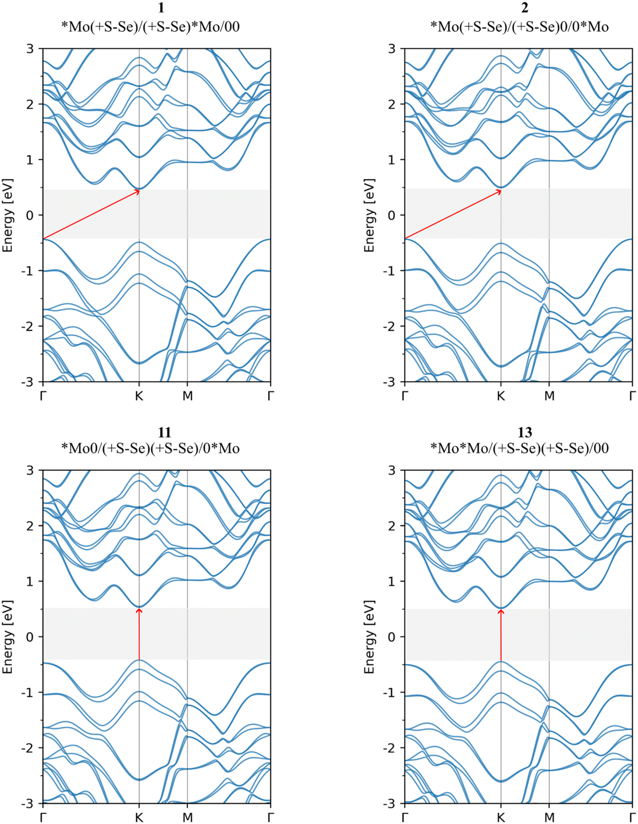 | ||
| Fig. 5 Electronic band structure of 1, 2, 11, and 13 stacking sequences of bilayer MoSSe. | ||
Only polytypes 11 and 13, with eclipsed S–Se pairs in interlayer interactions, retain a direct band gap similar to that of the monolayer, with both the conduction band minimum (CBM) and valence band maximum (VBM) at the K point. In contrast, the other configurations show indirect band gaps, with the VBM shifting to the Γ point (Fig. S3†), consistent with previous studies.12,13,16,17,37,38,40–42,44 The key distinction for polytypes 11 and 13 is their face-to-face S–Se interlayer distances, unlike those in polytype 1, where the S–Se interactions are lateral.
Interestingly, stacking arrangements with S–Se interactions and dipole moments correlate with lower bandgaps, ranging from 0.87 to 0.96 eV. The two most stable configurations, with dipole moments of 0.33 and 0.32 D, also have low bandgaps of 0.90 and 0.92 eV. Configurations with S–S interactions follow, with bandgaps from 0.97 to 1.27 eV, while those with Se–Se interactions have the highest bandgaps, from 1.32 to 1.50 eV. Electron density maps show minimal variation among the 16 bilayers (Fig. S4†), suggesting that interlayer interactions are mainly due to long-range dispersion forces.
To further explore the interlayer interactions, we performed a periodic energy decomposition analysis (PEDA).34 Although the interaction energies (ΔEint) from SCAN-D3/TZP vary modestly (−5.40 to −3.28 kcal mol−1), their ranking is consistent with that in SCAN-rVV10 predictions. An inverse relationship is found between the orbital contributions and Pauli repulsion: lower-energy configurations, with shorter interlayer distances, show higher orbital contributions (exceeding 29%, or −2.91 and −2.38 kcal mol−1) in sequences 1–9. In contrast, higher energy polytypes (with interlayer distances over 3.6 Å) have lower orbital contributions, from −1.97 to −0.96 kcal mol−1. As layers approach, Pauli repulsion increases.
On the other hand, the dispersion energy (ΔEdisp) is the main attractive force, contributing 37.0 to 59.9% of the total interaction energy (Table 2). Our analysis indicates that electrostatic and dispersion energies counterbalance each other. In higher-energy polytypes (11–16), ΔEdisp constitutes 54.3 to 59.9% of the interaction energy, reducing the electrostatic component to 17.5–24.4%. In contrast, in lower-energy polytypes (1–7), ΔEdisp contributes 37.0 to 41.0%, while the electrostatic term ranges from 28.2 to 33.2%. This pattern highlights the increasing role of van der Waals forces and the importance of medium- and long-range interactions in bilayers.
Conclusions
We extended the JAM notation—a linear string-based system—to cover four types of transition metal dichalcogenides (TMDCs): 1H, 1T, Janus 1H, and Janus 1T. This extension facilitates the reconstruction of honeycomb lattice structures and represents various stacking sequences, including those in materials with three-atom unit cells, like MoS2.Using this expanded JAM notation, we identified and characterized all possible stacking arrangements for MoSSe bilayers, a Janus TMDC. Sixteen distinct stacking configurations were evaluated for energetic stability and electronic properties, including bandgap variations. Three configurations showed competitive stability: *Mo(S–Se)/(S–Se)*Mo/00, Mo(S–Se)/(S–Se)0/0Mo, and *Mo(–S + Se)/(S–Se)*Mo/00, each with interlayer distances under 3.30 Å and indirect band gaps of 0.90, 0.92, and 1.32 eV, respectively, in contrast to the monolayer's direct gap of 1.52 eV. Our findings highlight how interlayer interactions and symmetry significantly impact the electronic nature of MoSSe bilayers, with S–Se interactions at eclipsed positions notably affecting band gap values and type.
PEDA calculations show that the lowest-energy, closest-spaced configurations have the highest orbital contributions, with dispersion energy as the dominant attractive force (37.0%–59.9% of the total interaction energy). Thus, interlayer distance is crucial for determining the stability and electronic properties, underscoring the importance of van der Waals forces and long-range interactions in 2D bilayer studies.
The expanded JAM notation is a robust tool for examining stacking sequences and advancing TMDC multilayer research. Mastering the stacking arrangements is essential for applications in optoelectronics. This work lays the foundation for future studies on diverse 2D materials, facilitating the design of novel materials with customized properties. Furthermore, the multilayer structures derived from JAM can be effectively analyzed via machine learning interatomic potentials, trained on smaller cases to predict properties for larger configurations, as demonstrated for the 2D material family.50,51
Data availability
The data supporting this article have been included as part of the ESI.†Conflicts of interest
There are no conflicts to declare.Acknowledgements
This work was funded by Conahcyt (Grant Conacyt Ciencia Básica y/o Ciencia de Frontera No. 320362, Proyecto Sinergia 1561802, and Grant #A1-S-45886). J. A. thanks Conahcyt for support through her Postdoc fellowship. Computations supporting this project were performed on High-Performance Computing systems at Cinvestav (Xiuhcoatl) and the Palmetto Cluster at Clemson University. This material is based on work supported by the National Science Foundation under Grant Nos. MRI# 2024205, MRI# 1725573, and CRI# 2010270.References
- M. Chhowalla, H. S. Shin, G. Eda, L.-J. Li, K. P. Loh and H. Zhang, Nat. Chem., 2013, 5, 263–275 CrossRef PubMed.
- E. S. Kadantsev and P. Hawrylak, Solid State Commun., 2012, 152, 909–913 CrossRef CAS.
- M. Calandra, Phys. Rev. B: Condens. Matter Mater. Phys., 2013, 88, 245428 CrossRef.
- A. N. Enyashin, L. Yadgarov, L. Houben, I. Popov, M. Weidenbach, R. Tenne, M. Bar-Sadan and G. Seifert, J. Phys. Chem. C, 2011, 115, 24586–24591 CrossRef CAS.
- H. Wang, Z. Lu, S. Xu, D. Kong, J. J. Cha, G. Zheng, P.-C. Hsu, K. Yan, D. Bradshaw, F. B. Prinz and Y. Cui, Proc. Natl. Acad. Sci. U. S. A., 2013, 110, 19701–19706 CrossRef CAS.
- L. Dong, J. Lou and V. B. Shenoy, ACS Nano, 2017, 11, 8242–8248 CrossRef CAS PubMed.
- Y. Guo, S. Zhou, Y. Bai and J. Zhao, Appl. Phys. Lett., 2017, 110, 163102 CrossRef.
- A.-Y. Lu, H. Zhu, J. Xiao, C.-P. Chuu, Y. Han, M.-H. Chiu, C.-C. Cheng, C.-W. Yang, K.-H. Wei, Y. Yang, Y. Wang, D. Sokaras, D. Nordlund, P. Yang, D. A. Muller, M.-Y. Chou, X. Zhang and L.-J. Li, Nat. Nanotechnol., 2017, 12, 744–749 CrossRef CAS.
- J. Zhang, S. Jia, I. Kholmanov, L. Dong, D. Er, W. Chen, H. Guo, Z. Jin, V. B. Shenoy, L. Shi and J. Lou, ACS Nano, 2017, 11, 8192–8198 CrossRef CAS PubMed.
- R. Li, Y. Cheng and W. Huang, Small, 2018, 14, e1802091 CrossRef.
- M. Meng, T. Li, S. Li and K. Liu, J. Phys. D: Appl. Phys., 2018, 51, 105004 CrossRef.
- Z. Guan, S. Ni and S. Hu, J. Phys. Chem. C, 2018, 122, 6209–6216 CrossRef CAS.
- L. Zhong, X. Li, Y. Pu, M. Wang, C. Zhan and X. Xiao, Phys. Chem. Chem. Phys., 2024, 26, 1030–1038 RSC.
- Q. Wu, L. Cao, Y. S. Ang and L. K. Ang, Nano Express, 2020, 1, 010042 CrossRef.
- B. Hou, Y. Zhang, H. Zhang, H. Shao, C. Ma, X. Zhang, Y. Chen, K. Xu, G. Ni and H. Zhu, J. Phys. Chem. Lett., 2020, 11, 3116–3128 CrossRef CAS PubMed.
- S. Wei, J. Li, X. Liao, H. Jin and Y. Wei, J. Phys. Chem. C, 2019, 123, 22570–22577 CrossRef CAS.
- B. Song, L. Liu and C. Yam, J. Phys. Chem. Lett., 2019, 10, 5564–5570 CrossRef CAS PubMed.
- C. Shang, X. Lei, B. Hou, M. Wu, B. Xu, G. Liu and C. Ouyang, J. Phys. Chem. C, 2018, 122, 23899–23909 CrossRef CAS.
- J. Arcudia, F. Ortíz-Chi, A. Sánchez-Valenzuela, A. Aspuru-Guzik and G. Merino, Matter, 2023, 6, 1503–1513 CrossRef.
- J. Arcudia, R. Kempt, M. E. Cifuentes-Quintal, T. Heine and G. Merino, Phys. Rev. Lett., 2020, 125, 196401 CrossRef CAS PubMed.
- J. Arcudia, B. Emrem, T. Heine and G. Merino, Nanoscale, 2022, 14, 10136 RSC.
- P. E. Blöchl, Phys. Rev. B: Condens. Matter Mater. Phys., 1994, 50, 17953–17979 CrossRef PubMed.
- G. Kresse and D. Joubert, Phys. Rev. B: Condens. Matter Mater. Phys., 1999, 59, 1758–1775 CrossRef CAS.
- G. Kresse and J. Furthmüller, Comput. Mater. Sci., 1996, 6, 15–50 CrossRef CAS.
- G. Kresse and J. Furthmüller, Phys. Rev. B: Condens. Matter Mater. Phys., 1996, 54, 11169–11186 CrossRef CAS PubMed.
- H. Peng, Z.-H. Yang, J. P. Perdew and J. Sun, Phys. Rev. X, 2016, 6, 041005 Search PubMed.
- M. Mazars, Phys. Rep., 2011, 500, 43–116 CrossRef CAS.
- J. P. Perdew, K. Burke and M. Ernzerhof, Phys. Rev. Lett., 1996, 77, 3865–3868 CrossRef CAS PubMed.
- A. Togo and I. Tanaka, Scr. Mater., 2015, 108, 1–5 CrossRef CAS.
- H. Li, J. Wu, Z. Yin and H. Zhang, Acc. Chem. Res., 2014, 47, 1067–1075 Search PubMed.
- X. Zhang, X.-F. Qiao, W. Shi, J.-B. Wu, D.-S. Jiang and P.-H. Tan, Chem. Soc. Rev., 2015, 44, 2757–2785 Search PubMed.
- G. te Velde, F. M. Bickelhaupt, E. J. Baerends, C. Fonseca Guerra, S. J. A. van Gisbergen, J. G. Snijders and T. Ziegler, J. Comput. Chem., 2001, 22, 931–967 CrossRef CAS.
- G. te Velde and E. J. Baerends, Phys. Rev. B: Condens. Matter Mater. Phys., 1991, 44, 7888–7903 CrossRef CAS PubMed.
- M. Raupach and R. Tonner, J. Chem. Phys., 2015, 142, 194105 Search PubMed.
- https://github.com/Theochem-merida/xjam.git . (Accessed August 29, 2024).
- G. Constantinescu, A. Kuc and T. Heine, Phys. Rev. Lett., 2013, 111, 036104 Search PubMed.
- C. Shang, B. Xu, X. Lei, S. Yu, D. Chen, M. Wu, B. Sun, G. Liu and C. Ouyang, Phys. Chem. Chem. Phys., 2018, 20, 20919–20926 CAS.
- W.-J. Yin, B. Wen, G.-Z. Nie, X.-L. Wei and L.-M. Liu, J. Mater. Chem., 2018, 6, 1693–1700 CAS.
- Y. Ji, M. Yang, H. Lin, T. Hou, L. Wang, Y. Li and S.-T. Lee, J. Phys. Chem. C, 2018, 122, 3123–3129 CAS.
- Y. Yang, Y. Zhang, H. Ye, Z. Yu, Y. Liu, B. Su and W. Xu, Superlattices Microstruct., 2019, 131, 8–14 CAS.
- F. Li, W. Wei, H. Wang, B. Huang, Y. Dai and T. Jacob, J. Phys. Chem. Lett., 2019, 10, 559–565 CAS.
- C. Long, Y. Dai, Z.-R. Gong and H. Jin, Phys. Rev. B, 2019, 99, 115316 CrossRef CAS.
- G. Chaney, A. Ibrahim, F. Ersan, D. Çakır and C. Ataca, ACS Appl. Mater. Interfaces, 2021, 13, 36388–36406 CrossRef CAS PubMed.
- X. Zhang, R. Pang, X. Hou and S. Wang, New J. Phys., 2021, 23, 013003 CrossRef CAS.
- Z. Jia, H. Zhang, X. Chen and W. Ding, J. Electron. Mater., 2023, 52, 2458–2465 CrossRef CAS.
- L. Lin, X. Hu, R. Meng, X. Li, Y. Guo, H. Da, Y. Jiang, D. Wang, Y. Yang and X. Yan, Nanoscale, 2024, 16, 4841–4850 RSC.
- B. Emrem, R. Kempt, K. Finzel and T. Heine, Adv. Theory Simul., 2022, 5, 2200055 CrossRef.
- S. Grimme, J. Antony, S. Ehrlich and H. Krieg, J. Chem. Phys., 2010, 132, 154104 CrossRef PubMed.
- J. Klimeš, D. R. Bowler and A. Michaelides, Phys. Rev. B: Condens. Matter Mater. Phys., 2011, 83, 195131 CrossRef.
- I. S. Novikov, K. Gubaev, E. V. Podryabinkin and A. V. Shapeev, Mach. Learn. Sci. Technol., 2021, 2, 025002 Search PubMed.
- B. Mortazavi, B. Javvaji, F. Shojaei, T. Rabczuk, A. V. Shapeev and X. Zhuang, Nano Energy, 2021, 82, 105716 CrossRef CAS.
- P. H. T. Philipsen, G. te Velde, E. J. Baerends, J. A. Berger, P. L. de Boeij, M. Franchini, J. A. Groeneveld, E. S. Kadantsev, R. Klooster, F. Kootstra, M. C. W. M. Pols, P. Romaniello, M. Raupach, D. G. Skachkov, J. G. Snijders, C. J. O. Verzijl, J.A. Celis Gil, J. M. Thijssen, G. Wiesenekker, C. A. Peeples, G. Schreckenbach and T. Ziegler, SCM BAND 2024.1, Theoretical Chemistry, Vrije Universiteit, Amsterdam, The Netherlands, http://www.scm.com Search PubMed.
Footnote |
| † Electronic supplementary information (ESI) available. See DOI: https://doi.org/10.1039/d4nr03696d |
| This journal is © The Royal Society of Chemistry 2025 |