
Radio frequency switching devices based on two-dimensional materials for high-speed communication applications
Fei
Xing
a,
Fangzhu
Qing
 *abc,
Mo
Zhou
d,
Congcong
Ning
bc,
Wanyi
Liao
a and
Xuesong
Li
*abc
*abc,
Mo
Zhou
d,
Congcong
Ning
bc,
Wanyi
Liao
a and
Xuesong
Li
*abc
aShenzhen Institute for Advanced Study, University of Electronic Science and Technology of China, Shenzhen 518110, China. E-mail: qingfz@uestc.edu.cn; lxs@uestc.edu.cn
bSchool of Integrated Circuit Science and Engineering (Exemplary School of Microelectronics), University of Electronic Science and Technology of China, Chengdu 611731, China
cState Key Laboratory of Electronic Thin Films and Integrated Devices, Chengdu 611731, China
dShenzhen College of International Education, Shenzhen 518000, China
First published on 17th April 2025
Abstract
Two-dimensional (2D) materials, with their atomic-scale thickness, high carrier mobility, tunable wide bandgap, and excellent electrical and mechanical properties, have demonstrated vast application prospects in research on radio frequency (RF) switch devices. This review summarizes the recent advances in 2D materials for RF switch applications, focusing on the performance and mechanisms of 2D material-based RF switch devices at high frequencies, wide bandwidths, and high transmission rates. The analysis includes the design and optimization of devices based on graphene, transition metal dichalcogenides, hexagonal boron nitride, and their heterojunctions. By comparing the key performance parameters such as insertion loss, isolation, and cutoff frequency of the switches, this review reveals the influence of material selection, structural design, and defect control on device performance. Furthermore, it discusses the challenges of 2D material-based RF switches in practical applications, including material defect control, reduction of contact resistance, and the technical bottlenecks of large-scale industrial production. Finally, this review envisions future research directions, proposing potential pathways for improving device performance through heterojunction structure design, multifunctional integration, and process optimization. This study is of great significance for advancing the development of high-performance RF switches and the application of communication technologies in 6G and higher frequency bands.
1. Introduction
In recent years, with the rapid development of 5G/6G technologies1,2 and satellite communications,3 the information and communication fields have advanced towards the internet of everything and global digital integration,4,5 driving profound transformations across multiple domains. RF switches, as key components for signal routing, isolation, and path management, play a crucial role in this process. They are widely used in wireless communication and radar systems to enable frequency band selection and signal switching between RF ports. The performance metrics of RF switches, such as insertion loss, isolation, and power handling capability, are critical to their applications, and achieving optimal performance requires balancing on-state resistance and off-state capacitance. In the future, with the increasing frequency and bandwidth of communication devices, especially with the advent of 6G technology, RF switches will face more challenges, demanding higher operating frequencies and more complex modulation schemes.6,7 However, current commercial switch devices, such as PIN diodes and field effect transistors (FETs), face the challenge of small size effects,8 while switches based on microelectromechanical systems (MEMS) and phase-change materials (PCM) suffer from large physical dimensions and high driving voltages,9 hindering device miniaturization and low-power realization.As novel materials with atomic-scale thickness, two-dimensional (2D) materials exhibit superior properties such as ultra-high carrier mobility and tunable electronic effects, making them highly advantageous for high-frequency and low-power applications.10,11 The atomic-scale thickness of 2D materials can reduce the on-resistance (RON) to below 10 Ω, while effectively lowering the off-capacitance (COFF) by reducing the overlap area between the 2D materials and the contact electrodes. This enables RF switches to achieve cutoff frequencies ranging from GHz to THz across a wide spectrum.12–15 Furthermore, 2D material-based switch devices are capable of maintaining stable switching states at zero power consumption and achieving fast switching speeds.16 This is crucial for low-power and high-performance RF devices in fields such as mobile communications, satellite communications, and radar systems. By optimizing control logic and circuit structure, the stability and reliability of 2D material-based RF switches can be further enhanced.17
There have been review articles on the principles and applications of traditional RF switches, and in response to the increasing technological challenges, recent studies have also explored the RF performance and application realization of novel switch devices.18,19 This review focuses on the recent advances in 2D-material-based (2DMB) RF switches, as comprehensively outlined in Fig. 1. Firstly, a concise introduction to the fundamental principles of RF switches will be provided. Then, typical RF switches based on graphene, transition metal dichalcogenides (TMDs), hexagonal boron nitride (h-BN), and heterojunctions of 2D materials will be discussed. Following this, the discussion will shift to the preparation of 2DMB RF switches. This encompasses aspects such as the synthesis of 2D materials, their transfer processes, and the fabrication of the actual devices. Afterward, the critical factors influencing the performance of 2DMB RF switches will be explored. Finally, an outlook on future research directions will be provided. Overall, this review aims to offer valuable insights and references for researchers working on 2DMB RF switches, thereby facilitating the future progress of high-speed wireless communication across diverse scenarios.
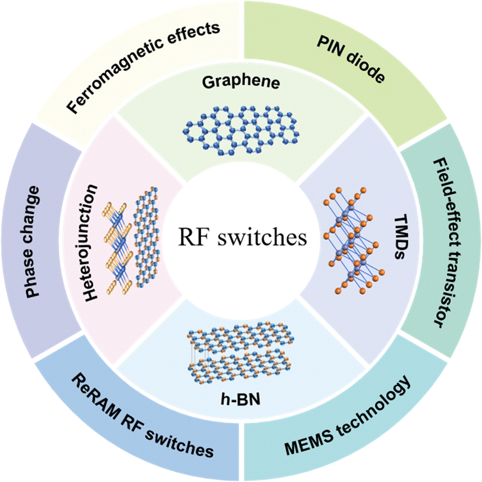 | ||
| Fig. 1 Overview of RF switches based on 2D materials. | ||
2. Principles of RF switches
To solve the switching loss caused by mechanical abrasion in traditional mechanical switches, solid-state RF switches have been designed based on semiconductor device principles, including PIN diodes, FETs, and hybrid PIN-FET switches. Additionally, emerging materials and processes have enabled the development of new switch types, such as MEMS, PCM, and memristor RF switches. Some new devices also incorporate non-volatile memory technologies, such as resistive random access memory (ReRAM), ferromagnetic RAM (FRAM), ferroelectric RAM (FeRAM), and spin-transfer torque RAM (STT-RAM) technologies. The non-volatile nature allows the devices to maintain their on/off states under zero power conditions, thus improving energy efficiency and integration.2.1. Architecture of RF switches
The architecture of RF switch devices is primarily categorized into two-terminal and three-terminal structures, both of which can be implemented using 2D materials. These devices typically operate in three modes: series connection in the RF signal path, parallel connection between the signal path and ground, or a combination of series and parallel configurations, with the series configuration being the most common (Fig. 2). | ||
| Fig. 2 Series circuits of RF switches: (a) two-terminal RF switches and (b) three-terminal RF switches. | ||
Two-terminal switches have an input terminal and an output terminal. They rely on specific physical mechanisms to control current conduction and cutoff, such as carrier injection modulation via the bias state of PIN junctions or resistance state switching in memristors (e.g., ReRAM, PCM, and FeRAM). Three-terminal switches, e.g., the FET switches, have a control terminal (gate) to control current conduction between the input and output terminals (source and drain). MEMS switches and hybrid devices, which incorporate mechanical displacement or heterogeneous integration, can be adapted to both two-terminal and three-terminal applications, further enhancing the design flexibility and adaptability of RF switches.
2.2. PIN diode
In the PIN diode, a thin layer of a lightly doped intrinsic semiconductor (the “I” layer) is inserted between the p-type and n-type semiconductor materials. Under the control of the excitation voltage, the space charge region of the p–i–n junction is changed to realize the switching state of the device. As shown in Fig. 3a, when the PIN diode is in a forward biased state, with the p terminal connected to a positive voltage and the n terminal connected to a negative voltage, carriers recombine in the I-layer, forming a low-resistance state. In reverse bias, the I-layer depletes, creating a high-resistance state. The low leakage current and high breakdown voltage make PIN diodes suitable for high-power RF applications.20 By adjusting forward current, the series RF resistance can be controlled, enabling applications like active gain control in wireless systems. This makes PIN diodes widely used in wireless communication, radar systems, and other fields.20,21 However, this type of RF switch has the disadvantages of low carrier injection efficiency and slow switching speed.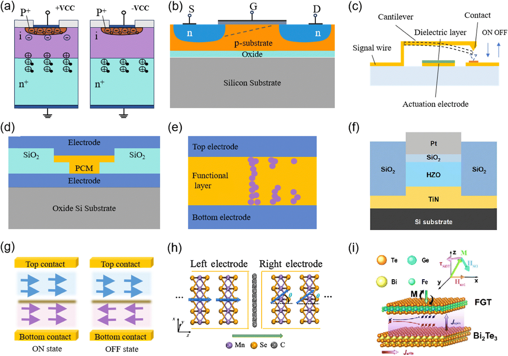 | ||
| Fig. 3 Schematic diagram of the RF switch working principles. (a) PIN diode. (b) MOSFET device structure. (c) MEMS. (d) PCM. (e) ReRAM. (f) FTJ. Reproduced with permission.22 Copyright 2024, Wiley-VCH GmbH. (g) MTJ. (h) MTJ driven by STT. Reproduced with permission.23 Copyright 2023, American Physical Society. (i) MTJ driven by SOT. Reproduced with permission.24 Copyright 2023, Springer Nature. | ||
2.3. Field-effect transistors
FET-based RF switches, especially MOSFETs (including CMOS, SOI, Fin-FETs, etc.), operate by controlling the conductive channel between the source and drain using gate voltage, as shown in Fig. 3b. This principle provides fast switching, high integration, and high frequency applicability.25,26 FET RF switches are suitable for use in 5G and Wi-Fi, but as MOSFET sizes continue to shrink, they face a series of severe challenges such as degradation of gate efficiency, increase of parasitic resistance and capacitance, and increase of the fabrication difficulty and cost.272.4. MEMS technology
MEMS RF switches reduce device size to the micron or nanometer scale and enable integration with sensors and circuits.28,29 They are categorized into resistive and capacitive types. Resistive switches have fast speeds and low driving voltages but face reliability issues and hysteresis. Capacitive switches offer better isolation but require higher driving voltages. As shown in Fig. 3c, common structures include cantilever and bridge configurations, with design optimizations like perforations and serpentine beams reducing actuation voltages.30–32 Despite high voltage limitations, electrostatic-driven capacitive MEMS switches show high isolation, wide bandwidth, and low loss. Simulation results have confirmed robust performance under high RF power.33 MEMS switches are widely applied in radar and satellite communications due to their low cost, reliability, and excellent RF performance.342.5. Phase change principle
As shown in Fig. 3d, phase-change memory (PCM) RF switches rely on reversible transitions between crystalline (low resistance) and amorphous (high resistance) states, induced by thermal or electrical pulses.35–37 GeTe-based PCM RF switches feature high cutoff frequencies, low insertion loss, and non-volatile properties.38,39 Using an Ag conductive filament as a heater reduces the contact area between the bottom electrode and GeTe, which reduces heat loss and achieves low energy consumption.40 Advances in fabrication processes have enabled integration of PCM switches with other RF components, further enhancing their potential for low-power, high-performance systems.41,42 However, PCM RF switches are subject to heating and cooling times and thermal stress cycles, resulting in slow switching speeds and poor device durability.2.6. ReRAM RF switches
A ReRAM utilizes mechanisms such as conductive filaments,43,44 space-charge-limited current,45 and Schottky barrier modulation46 for switching. As shown in Fig. 3e, under the influence of an electric field, ion migration forms conductive filaments, providing high and low resistance states for the switching function. In addition, the presence of traps or defects in the functional layer of a two-dimensional material and interfacial charge distributions can realize high and low resistive states by trapping or releasing charges and regulating the height of the potential barriers. There may be multiple mechanisms acting together in the switching state transitions of a resistive-variable memory. Initially, RF switches based on nanoscale memristors were composed of a pair of electrochemically asymmetric metal electrodes and a nanoscale air gap,9 with characteristics such as fast switching speed, low loss, and high isolation, operating at frequencies up to tens of GHz. A ReRAM features zero static power consumption, simple structure, and compatibility with CMOS processes. By combining a ReRAM with 2D materials (such as MoS2 or h-BN), device miniaturization and performance enhancement can be achieved. However, the durability and scalability47 of devices remain challenges for widespread application.2.7. Ferroelectric and ferromagnetic effects
Ferroelectric tunnel junctions (FTJs) and MTJs, as novel non-volatile RF switches, achieve high-performance signal switching based on electric-order and magnetic-order regulation mechanisms, respectively. FTJ devices are fabricated by sandwiching a ferroelectric layer between two electrodes. Based on the tunnel electroresistance (TER) effect, resistance state switching can be realized by modulating the barrier height through the polarization direction of the ferroelectric layer.48 Common ferroelectric layer materials include BaTiO3 and HfO2. Inserting a SrTiO3 layer into the BaTiO3 layer enhances its ferroelectricity, achieving an on/off ratio of 108.49 Additionally, for Zr-doped HfO2, the Pt/SiO2/HZO (Hf0.5Zr0.5O2)/TiN FTJ device structure exhibits durability exceeding 107 cycles (Fig. 3f).22MTJs adopt a ferromagnetic layer/insulating layer/ferromagnetic layer structure, where resistance is modulated through the spin-polarized tunneling magnetoresistance (TMR) effect. As shown in Fig. 3g, when the magnetization directions of the two ferromagnetic layers are parallel, the electron tunneling probability is high (low-resistance state), while in the antiparallel state, the probability sharply decreases (high-resistance state).50 The magnetization direction of MTJ devices can be controlled by spin transfer torque (STT) (Fig. 3h) or spin orbit torque (SOT) (Fig. 3i). STT directly injects a spin-polarized current into the free layer of the MTJ, utilizing angular momentum transfer to drive magnetization reversal. This two-terminal device structure is simple but requires a relatively high write current.23 In contrast, the three-terminal SOT device generates a transverse spin current through the spin Hall effect of a heavy metal layer (such as Pt or Ta) or the interfacial Rashba effect, driving the magnetization reversal of an adjacent ferromagnetic layer.24,51 With lower power consumption, higher switching speed, and excellent endurance, SOT has become the preferred solution for RF front-end applications.52
3. RF switches based on 2D materials
In the traditional RF switch devices, the performance of PIN and FET devices degrades due to the impact of small-size effects. When the device size is reduced to a certain extent, quantum effects such as electron tunneling and leakage currents arise, leading to degradation in device reliability and performance of the devices.27 Switch devices based on MEMS and PCM face challenges such as larger physical dimensions and higher driving voltages,9 making them difficult to meet the demands for miniaturization, integration, and low power consumption in future communication systems. Among new switch devices, ReRAM and ferroelectric devices exhibit poor switching durability, while magnetic memristors are unable to provide higher integration densities, hindering the commercialization of such devices.532D materials possess characteristics such as high carrier mobility, high thermal conductivity, high mechanical strength, and tunable bandgaps, which help improve the performance of RF switch devices, such as increasing switching speed, enhancing isolation, reducing power consumption, and widening bandwidth. Due to the excellent electrical properties and atomic-scale thickness of 2D materials, 2DMB RF switches can achieve zero static power consumption and device miniaturization, providing new solutions for high-performance RF switches. Table 1 lists the performance and working principles of RF switching devices based on typical 2D materials, including graphene, TMDs, h-BN, and their heterostructures.
| Materials | Mechanism/ref. | On/off ratio | V SET/VRESET (V) | Insertion loss (dB) | Isolation (dB) | Cutoff frequency (THz) | Power handling (dB m) | Switching time (ns) | Cycle endurance (cycles) | Switching energy (pJ) | Non-volatility |
|---|---|---|---|---|---|---|---|---|---|---|---|
| Graphene | NEMS54 | — | 1 | ∼0.015 | >40 | — | — | ∼4.03 × 10⁻³ | — | — | No |
| Graphene | —55 | 25–40 | 4/8 | — | — | — | — | — | 300 | — | — |
| Graphene | —56 | 104 | 2.5/−2.5 | — | — | — | — | — | — | — | Yes |
| Graphene | —57 | — | — | — | — | — | — | 2.60 × 10⁻⁴ | — | 0.035 | — |
| MoS2 | ReRAM12 | >103 | ∼1–1.2 | ∼0.3 | >20 | 11 | — | <30 | >20/100 | — | Yes |
| MoS2 | ReRAM14 | — | ∼1.5/−1.3 | ∼0.7 | ∼15 | 22 | — | — | — | 49 | Yes |
| WS2 | —58 | 103 | 1.62/−1.45 | — | — | — | — | — | 100 | — | Yes |
| ReSe2 | ReRAM59 | 103–104 | ∼2.5/−1 | — | — | — | — | — | >240 | — | — |
| MoS2 | —60 | 103 | 3.5–8.0 | — | — | — | — | — | — | — | — |
| WSe2 | FET61 | 107 | ∼2–3 | — | — | — | — | — | ∼1000 | — | No |
| h-BN | ReRAM13 | ∼106 | ∼1–3 | ∼0.27 | >35 | 129 | ∼20 | <15 | — | — | Yes |
| h-BN | ReRAM16 | — | — | — | — | — | — | 0.12 | ∼600 | 2 | Yes |
| h-BN | ReRAM62 | ∼105 | 1.5/−1 | <0.2 | ∼15 | 0.043 | ∼20 | <15 | — | — | Yes |
| h-BN | ReRAM63 | >10 | 0.66/−0.41 | — | — | — | — | ∼25 | — | ∼50 | Yes |
| h-BN | ReRAM64 | — | ∼3 | <2 | >30 | ∼4.7 | — | <2.5 | 103–104 | ∼600/∼172 | Yes |
| h-BN | ReRAM65 | 1011 | 0.33/−0.11 | ∼0.5 | >23 | ∼38 | ∼20 | — | 30 | 1200 | Yes |
| h-BN | QCATS66 | ∼106–109 | 0.3 | — | — | — | — | 50 | >107 | — | — |
| Graphene/hBN | ReRAM67 | >108 | ∼70 | >104 | Yes | ||||||
| WS2/MoS2 | ReRAM68 | 104 | 1.53/−1.51 | — | — | — | — | — | >120 | — | Yes |
| WTe2/α-In2Se3 | FTJ69 | 4.7 × 10⁵ | <2 | — | — | — | — | — | — | — | — |
| ReS2/WS2 | ReRAM70 | >106 | ∼2.9 | — | — | — | — | — | 200 | — | Yes |
3.1. Graphene-based RF switches
Graphene has high carrier mobility, high carrier saturation velocity and high thermal conductivity,71,72 which improve the high frequency performance of PIN and FET devices. Based on the PIN diode structure, studies have been conducted on metal–insulator–graphene (MIG) diodes73–75 and graphene–silicon (Si) Schottky diodes.76 The former control the current through tunneling or thermionic emission across the insulating barrier, while the latter affects carrier transition through the Schottky barrier formed at the graphene–Si interface. Both devices feature low forward turn-on voltage, which is beneficial for reducing power consumption. In particular, Schottky barrier diodes exhibit rapid switching speeds, making them more suitable for RF switch circuit designs.77For FET devices, the cutoff frequency is an important parameter for the device in RF switching applications. Graphene is difficult to use for semiconductor materials and gate dielectric materials because of its zero bandgap, but because of its high conductivity characteristics, graphene is often used for the improvement of conductive channels to improve conductivity and the high-frequency characteristics of devices. Graphene transistors prepared on silicon carbide substrates have the highest intrinsic cutoff frequency of 100 GHz (Fig. 4a).78 By a self-alignment process, the highest cutoff frequencies of graphene transistors fabricated on silicon/silicon oxide and glass substrates are 300 GHz and 427 GHz.79,80 The process solves the problem of lattice damage during device fabrication, reduces the contact resistance and parasitic capacitance of the device, and is equally applicable to other 2D materials.80,81 Moreover, the RF performance of graphene FETs is expected to be enhanced up to the terahertz band as channel lengths (<100 nm)82 are reduced and graphene quality is improved.81,83
 | ||
| Fig. 4 (a) Measured small-signal current gain |h21| as a function of frequency for a 240 nm gate and a 550 nm gate graphene FET at VD = 2.5 V, with the extrapolated cut-off frequencies of 53 GHz and 100 GHz for the 550 nm and 240 nm devices, respectively. The inset is a schematic cross-sectional view of a top-gated graphene FET. Reproduced with permission.78 Copyright 2010, American Association for the Advancement of Science. (b) Schematic of a graphene RF NEMS capacitive switch. Reproduced with permission.54 Copyright 2024, Springer Nature. (c) Suspended graphene device in the on and off states. The scale bar is 1 μm. Reproduced with permission.55 Copyright 2012, American Chemical Society. (d) Schematic structure and I–V characteristic curve of single-layer graphene sheet devices. Reproduced with permission.56 Copyright 2016, American Chemical Society. (e) Schematic of the graphene-loaded metal–insulator–metal (MIM)- waveguide. Reproduced with permission.57 Copyright 2019, Springer Nature. | ||
Graphene-based RF switches with other working mechanisms have also been reported. L. Zheng et al. reported a single-layer graphene RF switch prepared using NEMS technology, which exhibited a pull-in voltage of 1 V and a switching time of 4.03 ps in the DC to 140 GHz ultra-wideband (UWB) frequency range (Fig. 4b).54 H. Zhang et al. reported a suspended graphene switch where the switching mechanism originates from atomic motions and/or chemical rearrangements (Fig. 4c).55 M. Park et al. reported binary and ternary capacitive switching behaviors based on charge trapping and release in graphene (Fig. 4d).56 M. Ono et al. reported ultrafast and low-energy all-optical switching that was realized using graphene-loaded deep-subwavelength plasmonic waveguides (Fig. 4e).57
3.2. TMD-based RF switches
In RF switching applications, TMDs are mostly used in MIM-structured memristor devices. The resistive switching based on TMDs exhibits high switching ratios and low set voltages, with the switching mechanism mainly attributed to the migration of metal ions or oxygen vacancies in the conductive filament mechanism.58,59,84 M. Kim et al. reported a zero-static power MoS2 atomic device utilizing a ground-signal-ground (GSG) structure, realizing a nanoscale non-volatile RF switch (Fig. 5a and b).12 At an operating frequency range of 0–50 GHz, both single-layer and bilayer MoS2 switching devices exhibited bipolar resistive switching effects with low insertion loss and high isolation (Fig. 5c and d). Furthermore, the single-layer MoS2 switch device demonstrated excellent linearity exceeding 20 dB m in the ON state (0.25 × 0.5 μm2, 1 GHz) and an observed self-switching state at 11 dB m in the OFF state (0.5 × 0.5 μm2, 3 GHz). By scaling the area of the vertical parallel plate capacitor structure and optimizing the coplanar waveguide (CPW) design, M. Kim et al. optimized the MoS2 RF switch, achieving the operating bandwidth up to 480 GHz, meeting the requirements for 6G communication technology.14 The MoS2 RF switch achieved real-time data communication at 100 Gbit per s with a low bit error rate (BER) and a high signal-to-noise ratio (SNR) at a carrier frequency of 320 GHz. When comparing the fundamental signal and the third-order intermodulation products with IMD visual indicators, the slopes were 1 and 3, respectively, indicating good linearity of the MoS2 RF switch. Beyond MoS2, other TMDs have also been investigated. For example, U. Das et al. reported the Al/WS2/Pt device exhibiting a switching ratio of 103 and endurance over 100 cycles.58 | ||
| Fig. 5 (a) Zoomed-in plane view SEM image of a MoS2 RF switch with a lateral area of 1 × 1 μm2. Scale bar, 2 μm. The inset shows the optical microscopy image of the device. (b) Equivalent circuit diagram of an MoS2 RF switch. (c) Insertion loss based on single-layer MoS2 RF switches. (d) Isolation based on single-layer MoS2 RF switches. (a)–(d) Reproduced with permission.12 Copyright 2018, Springer Nature. (e) Schematic of an intersecting-GB MoS2 memristor. (f) Partial I–V characteristics of an electroformed intersecting-GB memristor (channel length, L = 7 μm). The set process occurs at Vset = 8.3 V with an abrupt twofold increase in current. Inset: full I–V characteristics of one switching cycle. (e) and (f) Reproduced with permission.60 Copyright 2015, Springer Nature. (g) Schematic of the TMD based microcavities, consisting of WS2-superlattices sandwiched between two DBRs. (h) The angle-resolved reflectivity map of the superlattice microcavity. (g) and (h) Reproduced with permission.85 Copyright 2024, Springer Nature. | ||
In addition to the conductive filament mechanism, V. K. Sangwan et al. reported that grain boundary (GB) triggering could also achieve resistance modulation (Fig. 5e and f).60 The three-terminal MoS2 memristor modulates the gate voltage (0–40 V) to achieve adjustable setup voltage (3.5–8.0 V) and resistance, with switching ratios up to 103. Resistance of TMDs can also be tuned by phase transition between the semiconductor 2H phase and the quasi-metallic 1T phase. Compared to the slow phase transition at room temperature and atmospheric pressure, J. Lim et al. increased the phase transition speed by low-power illumination, providing potential for future ultra-high-frequency signal communication.86
Due to their high exciton binding energy and robust valley degree of freedom, single-layer TMDs are also considered an ideal platform for developing room-temperature spintronic devices. J. Zhao et al. reported a microcavity structure constructed based on WS2 superlattices, utilizing strong coupling effects to achieve on/off spin switching states within 1 ps by altering the polarization state of the control light (Fig. 5g and h).85
Since TMD materials possess a large bandgap and lack dangling bonds, TMD-based RF switches with FET structure have also been developed. T. Zou et al. reported a Br2-doped WSe2 p-type transistor, which effectively reduced the contact resistance through interfacial doping, with a threshold voltage close to zero volts and a current on/off ratio in excess of 107.61 However, contact resistance remains a critical factor affecting FET device performance. For thin-layer MoS2 n-MOSFETs and WSe2 p-MOSFETs, the use of the half-metal PtSe2 as a contact layer also significantly reduces the contact resistance, showing excellent conductivity compared to conventional Ti/Au contacts.87 The use of metal–insulator–semiconductor contacts at the metal/MoS2 interface can improve the current drive capability and breakdown voltage of MoS2 transistors.88 Additionally, by employing molecularly functionalized ionic liquids, reversible electrochemical switching was realized on the MoS2 surface. This device further enhances FET performance by suppressing electron scattering at defect sites and reducing contact resistance via molecular doping effects, achieving a field-effect mobility of approximately 116 cm2 V−1 s−1 for single-layer MoS2.89
3.3. h-BN-based RF switches
h-BN is an excellent electrical insulator with high breakdown voltage and high thermal stability for high-frequency, high-voltage, and high-temperature insulation applications.90–94 The h-BN RF switches are also often used in MIM-structured memristor devices. M. Kim et al. reported an Au/h-BN/Au switch based on single-layer h-BN, which offers advantages such as non-volatility and nanosecond-scale magnetic levitation bearings, facilitating heater-free and simple planar integration. This switch operates at frequencies up to 110 GHz, covering RF, 5G, and millimeter-wave bands and exhibits excellent potential for low-power switches.62 The same group further demonstrated that the single-layer h-BN switch could operate across a frequency range of 0.1 to 200 GHz, maintaining low insertion loss (≤0.5 dB) and high isolation (≥10 dB) (Fig. 6a).13 They also showed that at 100 GHz, the h-BN switch achieves a data transmission rate of 8.5 Gbit per s with a BER below 10−10 (Fig. 6b), demonstrating its potential in future high-speed communication systems.13,62 | ||
| Fig. 6 (a) Measured higher-frequency S-parameter (S21) data and model line into the terahertz range. (b) BER measurements with different switch status. Insets: eye diagrams measured at fc = 100 GHz with a bit rate of 8.5 Gbit per s show a similar on-state BER after a switching cycle. (a) and (b) Reproduced with permission.13 Copyright 2020, Springer Nature. (c) Schematic diagram of the proposed resistive switching mechanism. (i) Pristine state: h-BN film contains structural defects (homoelemental B–B bonds, VN). (ii) Set transition: under a forward bias, Tix+ ions from the active Ti electrode are penetrated across the h-BN film toward the Au electrode, leading to the formation of conductive filaments. (iii) Reset transition: under a reverse bias, Ti-based conductive filaments are dissolved by the opposite polarity bias while Tix+ ions are retracted back to the Ti electrode. Reproduced with permission.63 Copyright 2020, American Chemical Society. | ||
Few-layer h-BN also exhibits excellent resistive switching characteristics.63 H. Jeong et al. designed a device structure of Au/Ti/h-BN/Au/Ti, where the top Au layer acts as a protective layer and the bottom Ti layer acts as an adhesion layer. This device shows significant bipolar resistive switching behavior without an initial electroplating process. The resistive switching mechanism is attributed to homogeneous B–B bonds and nitrogen vacancies at the grain boundaries of h-BN, which provide preferential channels for Tix+ ions to penetrate into the h-BN film and form conductive filaments (Fig. 6c).63 The memristor switch composed of titanium and 7–8 layers of h-BN exhibit ultra-fast switching characteristics with an average switching time of 1.43 ns under short voltage pulses (<3 ns).16 To further improve the switching performance of the device, S. Pazos et al. reduced the open-state resistance (∼4.5 Ω) by optimizing the electrode material and improving the conductivity, resulting in a loss of less than 2 dB at 260 GHz. Moreover, in combination with series-parallel logic circuits, the switch achieves more than 35 dB isolation at 120 GHz, demonstrating the reliability and performance benefits of complex RF circuits.64
To further optimize the switching performance, S. J. Yang et al. used Ag to replace the inert Au electrode, fabricating the Ag/h-BN/Ag switch. Lower switching voltage (<0.34 V) and leakage current (<23 fA) were achieved, demonstrating low static energy consumption. Furthermore, by restricting the current (100 μA–10 mA), the switching ratio and insertion loss can be adjusted.65
By utilizing single-atom boron defects to form single-atom point contacts in the hBN layer, R. D. Nikam et al. reported the quantized conductance atomic threshold switch device made from atomic-thin hBN layers, which showed stable and reproducible quantized conductance states at 1G0.66 The switching mechanism has been confirmed through in situ visualization of single-atom conductive filaments. The switching mechanism is mainly affected by atomic defects in h-BN, and by reducing the area and thickness of the switching region to form single-atom point contacts, the switching characteristics can be improved.
Density functional theory and machine learning potential model calculations show that the ferroelectricity of h-BN bilayers is controlled by interlayer sliding. Its spontaneous polarization originates from charge transfer rather than ionic displacement, with ultra-low ferroelectric switching barriers and high thermal stability. Utilizing domain wall motion can reduce the critical ferroelectric switching field of a single-domain by two orders of magnitude, enabling domain switching on the picosecond time scale.95
3.4. Heterojunction-based RF switches
Compared to the performance imbalance of a single material, heterojunctions combine the characteristics of different materials, forming structures with optimal electrical, optical, and mechanical properties, while reducing interface defects, which is beneficial for the development of high-performance RF switch devices.R. D. Nikam and H. Hwang reported a graphene/h-BN based atomic threshold switch (TS), where graphene acted as an ionic transport layer to control Ag ion injection, achieving superior volatile switching characteristics, with an on/off ratio >108, switching time as short as 70 ns, and durability >104 cycles. In the MIM structured h-BN TS device without a graphene layer, a high flux of Ag ions from the top electrode results in random formation of Ag filaments, leading to severe variation in the selector switching characteristics. In contrast, the graphene layer with atomic defects helps constrain the size of conducting filaments and prevent the formation of unwanted filaments (Fig. 7a).67
 | ||
| Fig. 7 (a) Schematic illustration of monolayer graphene ionic barrier and its impact on the Ag atomic threshold switch that uses single-layer hBN. Reproduced with permission.67 Copyright 2022, Wiley-VCH GmbH. (b) Schematic diagrams of the resistance switching mechanism of the WS2/MoS2 heterojunction memristor (top) and the evolution of the band structures (bottom). Reproduced with permission.68 Copyright 2021, RSC Pub. (c) Schematic diagrams of the resistive switching mechanism for the ReS2/WS2-based planar memristor. Reproduced with permission.96 Copyright 2023, Wiley-VCH GmbH. (d) Schematic of the three different polarization states, corresponding to the three resistance levels in the WTe2/α-In2Se3/Au FSJ device (top) and the corresponding band diagrams (bottom). Reproduced with permission.69 Copyright 2025, American Chemical Society. | ||
The diversity of TMDs provides more possibilities for the preparation and performance control of heterojunctions. W. Zhang et al. reported a WS2/MoS2 heterojunction that can achieve resistive switching based on band modulation rather than conductive filaments, avoiding material degradation during switching, thereby improving the durability of the device (Fig. 7b).68 F. Huang et al. reported a scalable 2D planar memristor based on the ReS2/WS2 heterojunction, which further enables optical control of resistive switching by controlling the interlayer charge transfer inside the heterojunction (Fig. 7c).96 Y. Li et al. reported the fabrication of a ferroelectric semiconductor junction (FSJ) by incorporating a ferroelectric metal as one of the electrodes with a WTe2/α-In2Se3/Au device structure (Fig. 7d).69 Transverse switching devices prepared based on this heterojunction achieve switching ratios of 105–106, low switching voltages (<2 V), and low leakage currents (∼10−12 A).69,70
3.5. Other 2D materials for RF switches
Some other 2D materials also show potential applications for RF switches. For example, black phosphorus (BP) has demonstrated both high carrier mobility (6500 cm2 V−1 s−1) and on/off ratio (106).97 J. Lin et al. designed a MoS2 transistor based on a black-scaled BP filamentary threshold switching resistor, achieving an on/off ratio of 107, which makes it suitable for low-power circuits and monolithic integration.98 Among telluride materials, highly crystalline MTe2 nanosheets exhibit a giant magnetoresistance effect and excellent performance as electrodes for micro-supercapacitors.99 Amorphous carbon (a-C) thin films can optimize their electrochemical performance by tuning thickness, doping concentration, and the sp2/sp3 bond ratio, while oxidized amorphous carbon (a-COx) exhibits controllable electrochemical switching behavior based on redox reactions.100 Additionally, a 2D perovskite ((PEA)2PbI4) single-crystal memristor fabricated using an improved space-confined method achieves an on/off ratio of 103 under a compliance current of 10−7 A, demonstrating the potential for device miniaturization.101These high-performance metrics provide new pathways to reducing the power consumption of traditional silicon-based RF switches. However, in practical applications, the stability and uniformity of devices based on these materials still need improvement. Through material doping, interface engineering, and process optimization, these limitations are expected to be partially overcome, driving 2D memristors toward high-frequency, low-power RF switching applications.
4. Preparation process of RF switches based on 2D materials
In contrast to the CMOS technology, where each functional layer is directly deposited on the substrate, 2D materials are typically synthesized separately and then transferred to the target substrate for further fabrication. Consequently, both the synthesis and transfer processes of 2D materials are equally critical to the overall device fabrication.4.1. Preparation of 2D materials
Typical preparation methods are illustrated in Fig. 7. In laboratory settings, the most common and straightforward 2D materials preparation method for small-scale experimental prototype verification is the scotch tape method, also known as the micro-mechanical exfoliation method.102 This technique involves peeling single or few-layer 2D materials from bulk materials, yielding high-quality samples suitable for initial testing and proof-of-concept studies.For large-scale industrial production of high-quality 2D material films, chemical vapor deposition (CVD) technology stands out as the most popular method. In CVD processes, gaseous precursors containing the required elements react under high-temperature conditions on a solid substrate, decomposing and depositing to form continuous 2D material films (Fig. 8a and b). Graphene and hBN films are mainly grown on Cu substrates,103,104 while TMDs on dielectric substrates such as SiO2/Si105 and sapphire.106 By controlling parameters such as temperature, pressure, atmosphere, and the substrates, researchers can fine-tune the material crystallinity, thickness, and defect density.107,108 This level of control has led to significant advancements, including the production of wafer-scale single crystals of graphene,109,110 hBN,111,112 and TMDs113,114 like MoS2 and WSe2. These achievements demonstrate the potential for large-scale applications of 2D materials through optimized epitaxial growth on single-crystalline substrates with desired surface orientations.
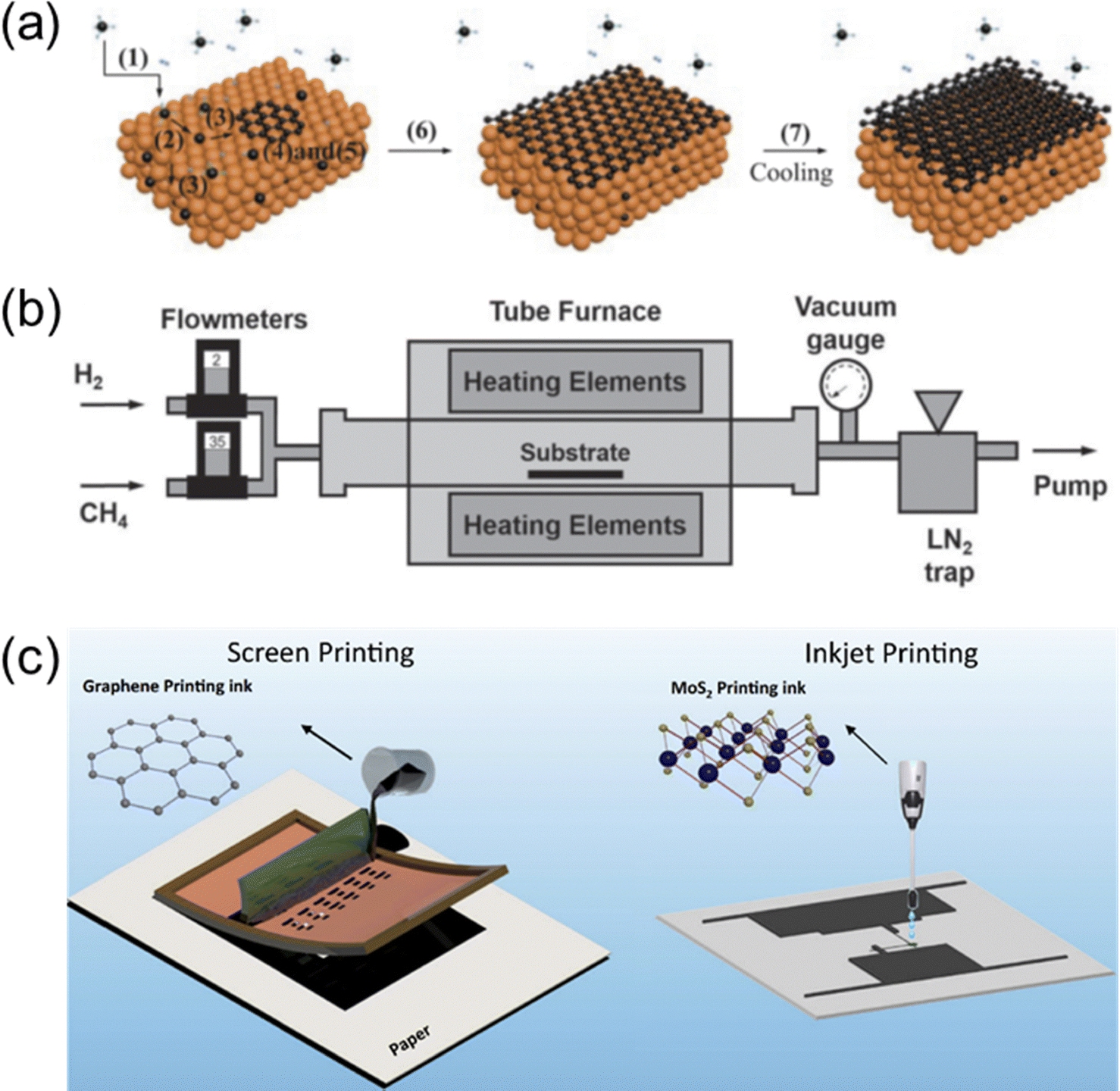 | ||
| Fig. 8 (a) Schematic of 2D material growth kinetics in the CVD process (taking the growth of graphene on the Cu substrate as an example). Reproduced with permission.115 Copyright 2017, The Materials Research Society. (b) Schematic of typical CVD equipment. Reproduced with permission.116 Copyright 2016, John Wiley and Sons. (c) Printing methods. Reproduced with permission.117 Copyright 2024, Springer Nature. | ||
In addition to CVD, printing methods such as spin coating118 and inkjet printing117 of liquid-phase exfoliated nanoflake solutions offer alternative approaches for preparing thin 2D material films (Fig. 8c). Compared to CVD, these techniques allow for a low-cost process at room temperature and enable integration onto flexible substrates, facilitating the development of flexible devices.
4.2. Transfer of 2D materials
For the device fabrication, the general transfer process is mainly associated with the shift from the growth substrate to the target by using a carrier material on the surface of 2D materials as a supporting layer (SL) (Fig. 9). The SL is applied to protect the 2D material during the removal of the original substrate, by chemical coating of a polymer (commonly polymethyl methacrylate, PMMA)103,119,120 or mechanical lamination of an adhesive tape.121,122 Once the SL is placed, the original substrate is etched by dissolving in an etchant103,120 or detached mechanically121,123 or electrochemically,124,125 leaving the 2D material attached to the SL. The 2D-material/SL stack is then transferred to the target substrate, which is typically a silicon wafer, glass, or another material suitable for device fabrication. Finally, the SL is removed, either by dissolving it in a solvent103,119 or by mechanically peeling it away,126 to leave the 2D material on the target substrate.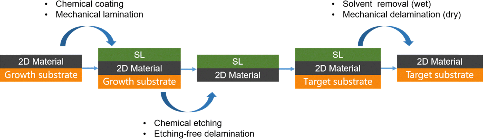 | ||
| Fig. 9 Schematic illustration of the general transfer strategies of 2D materials. | ||
The transfer strategies can be classified as wet transfer and dry transfer according to whether a liquid is involved during the transfer process. Since the fabrication of devices is mainly correlated to the step of removing the SL, sometimes transfer is considered as wet or dry simply according to whether a liquid is involved in the steps of placing the 2D-material/SL stack on the target substrate and removing the SL, regardless of how the growth substrate is removed. Wet transfer offers precise control and compatibility with various target substrates but is time-consuming and may introduce contamination or residues, potentially degrading the material's properties. Dry transfer, on the other hand, avoids solvent-related issues and the operation is convenient, making it suitable for large-scale manufacturing. However, it risks introducing defects or damaging the fragile 2D material.
4.3. Device fabrication
In general, there are two strategies for the fabrication of 2DMB devices. One is to pattern each functional layer by lithography in a layer-by-layer process. For example, to make a bottom-gated 2D FET, the 2D material is firstly transferred to the target substrate and then patterned, followed by the deposition of metal electrodes (source and drain).127 However, the lithography process usually causes contamination of the surface of 2D materials and the deposition of metal (e.g., by electron beam evaporation or sputtering) tends to destroy the structure of 2D materials.128,129 To address this issue, a transfer fabrication strategy has been developed. It patterns each functional layer separately on different substrates and then transfers one to another.122,130 This method can optimize the van der Waals contact between the metal electrode and the 2D material, maintain the intrinsic electric transport characteristics, effectively realize the universal fabrication of 2D electronic devices and extend to the wafer scale.122 However, since this method requires peeling off the metal electrodes from another substrate, it is currently limited to specific metals (Au, Pt, Pd, and Al). Many metals with low contact resistance, such as Ti and Cr, exhibit strong adhesion to the substrate and lack the low-energy surfaces necessary for forming metal–substrate van der Waals interfaces, making them difficult to be cleanly detached via standard dry transfer techniques.1315. Factors affecting RF switching performance based on 2D materials
5.1. Device structure
To achieve a high cutoff frequency, the on-resistance (Ron) and off-capacitance (Coff) of the switch device should be as small as possible. In the vertical MIM structure, an increase in the thickness of the 2D material results in the increase of both Ron and Coff, which increase the insertion loss and decrease the cutoff frequency. The increase of resistance is due to the increase of the conductive channel. The increase of capacitance is due to the increase of the dielectric constant (Fig. 10a).132 However, to keep the switch isolation the functional layer cannot be too thin. There is a trade-off between low loss and high isolation. Increasing the compliance current can also reduce the insertion loss,12 but the current capacity of interconnects needs to be considered. In the Au/h-BN/α-In2Se3/graphene heterojunction memristor switches, the thickness of the h-BN intermediate layer is a key parameter in modulating the interface Schottky barrier, which influences the off-state current level (Fig. 10b).46 In a study of encoded RF/microwave reconfigurable graphene hypersurfaces on MoS2 flexible substrates, the set voltage of Ag/MoS2/Ag switches can be reduced and optimized by controlling the thickness of the MoS2 layer and the switch structure.117 | ||
| Fig. 10 (a) Permittivity deduced from MIM, which increases with the numbers of layers. The blue circles and red squares represent two different batches of samples. Reproduced with permission.132 Copyright 2015, American Chemical Society. (b) The vacancy migration model and energy band diagram reveal the effect of h-BN thickness on the Au/h-BN/α-In2Se3/graphene heterojunction memristor switch. Reproduced with permission.46 Copyright 2023, Wiley-VCH GmbH. | ||
The overlapping area of the MIM structure is also an important factor affecting the high-frequency performance of the switching devices. In FET, PCM, and MEM switches, RON is inversely proportional to the area, while COFF is directly proportional to the area, leading to a trade-off where the area is reduced at the cost of insertion loss and isolation. In switches based on atomic-scale thin materials, RON is independent of the area, while COFF is directly proportional to the area.12,62 By reasonably controlling the overlap area and utilizing the low dielectric constant characteristics of 2D materials, the off-capacitance can be minimized so as to increase the cutoff frequency.
5.2. Contact resistance
The contact resistance (Rc) between the 2D materials and the metal electrodes, which is sometimes larger than that of the functional layer and contributes to the total Ron, significantly affects the conduction performance. For an ideal metal–TMD contact, a moderate interface coupling strength is required to balance the Fermi level pinning effect and carrier tunneling efficiency.133 Firstly, the choice of materials directly impacts the barrier height. Based on the density functional theory calculation system, M. Y. Gong et al. screened out bulk silver (Ag) as the most ideal contact electrode material for n-type MoS2 devices, with a contact resistance as low as 83 Ω μm.133 Z. Sun et al. changed the metal deposition environment and found that the strong bonding interaction between Ni and MoS2 under ultra-high vacuum conditions can reduce the contact resistance, while Bi is hardly affected by the deposition environment.134 To further reduce the contact resistance, semi-metallic platinum diselenide (PtSe2) or the two-dimensional material itself (such as MoS2) is used to replace the traditional Ti/Au metals as the contact layer.69,70,87 By enhancing the orbital hybridization between the semi-metal and the two-dimensional semiconductor interface, the contact resistance of the prepared Sb(0112)–MoS2 heterostructure is only 42 Ω μm, which is lower than that of silicon-based devices for the first time and close to the theoretical quantum limit, and it also has excellent stability at 125 °C.135 Using molecular beam epitaxy technology to form an atomically smooth contact interface or by introducing nano-confined polarized water molecules to enhance the interface interaction can also achieve a reduction in contact resistance.136,137 The design of control electrodes into small-sized nanowire structures can realize strong electrostatic control, which is expected to reduce the contact resistance and increase the cutoff frequency.1385.3. 2D material defects
The types of defects in 2D materials mainly include lattice defects (such as vacancies and dislocations), impurity doping, and surface roughness.107 Lattice defects can cause carrier scattering, increase resistance, and reduce the device's conduction performance. Surface roughness or contamination can lead to an increase in the contact resistance.In particular, electronic devices that drive current uniformly along the plane of 2D layered materials (i.e., transistors and lateral memristors) are strongly influenced by local defects (i.e., grain boundaries, wrinkles, thickness fluctuations, and polymer residues). In contrast, vertical devices are less affected because the current generated in the device flows through the out-of-plane and is always driven by the most conductive local positions.139 The growth conditions can be optimized to improve the crystallinity of the material. Surface modifications140 and encapsulation techniques141 can reduce surface contamination. In addition, the material transfer process must be precisely controlled to avoid introducing additional defects or contamination during the transfer process.142–144
The bandgap of 2D materials mainly affects the leakage current and switching ratio of the switch device. Wide bandgap materials (such as h-BN, ∼6 eV) are more suitable for high isolation and high-power handling requirements, but the on-resistance may be higher. Narrow bandgap materials (such as MoS2, ∼1.2 eV) perform better at low voltages, but the off-state capability is relatively weak. The precise adjustment of the bandgap can be achieved through defect engineering, e.g., by introducing sulfur vacancies to tune the MoS2 bandgap.145
5.4. Temperature
With the increase in device density and integration, effective heat dissipation under operating conditions has become a crucial factor influencing device performance. At high temperatures, the thermal stability of materials may decrease, leading to a decline in electrical conductivity, and the defect density of some 2D materials may also increase with rising temperature. For example, in memristor devices, the increase in temperature reduces the difference between the high and low resistance states, thereby decreasing the switching ratio and increasing insertion loss.146 Moreover, the anisotropic thermal transport properties of 2D materials play a role in controllable heat transfer and smart thermal management.1476. Conclusions and perspectives
This review explores 2DMB RF switches, discussing various device architectures, performance metrics, and fabrication techniques and emphasizing the potential of 2D materials to outperform traditional semiconductors in terms of speed, power consumption, and scalability.Despite the promising attributes of 2D materials, several challenges hinder their widespread adoption in RF switches. Firstly, achieving consistent material quality and uniformity over large areas is still challenging, even for the early developed materials such as graphene and h-BN, which affects device performance and reliability. Secondly, the integration of 2D materials into existing semiconductor manufacturing processes remains complex and costly. In particular, the transfer process is almost inevitable, which causes materials damage and contamination. Thirdly, the contact resistance between 2D materials and metal electrodes is often high, limiting the overall efficiency of the switches. Additionally, device endurance is poor due to the instability of 2D materials. Finally, there is a lack of comprehensive models and simulation tools to accurately predict the behavior of 2DMB RF switches, which slows down the design and optimization process.
To address these challenges, several strategies can be employed. Firstly, advancements in material synthesis techniques, such as improved CVD method, can help achieve higher-quality and more uniform 2D materials over larger areas. Additionally, the development of direct growth methods on target substrates could eliminate the need for transfer processes, thereby reducing material damage and contamination. Secondly, innovative integration approaches, such as van der Waals integration and hybrid bonding, can facilitate the seamless incorporation of 2D materials into existing semiconductor manufacturing workflows. Thirdly, surface engineering and interface optimization techniques, including the use of interfacial layers or doping, can significantly reduce contact resistance between 2D materials and metal electrodes. Encapsulation methods, such as atomic layer deposition (ALD) of protective layers, can enhance the environmental stability and endurance of 2D materials. Finally, the development of advanced theoretical models and simulation tools, leveraging machine learning and multiscale modeling, can accelerate the design and optimization of 2DMB RF switches.
The future of 2D materials in RF switch applications is promising, with several key directions for research and development. Scalable and cost-effective fabrication techniques will be critical to enabling the mass production of high-quality 2D materials. Innovations in direct growth and transfer-free processes will play a pivotal role in overcoming integration challenges. Furthermore, the exploration of novel 2D materials, such as Janus structures and heterostructures, could unlock new functionalities and improved performance. Collaborative efforts between academia and industry will be essential to bridge the gap between laboratory discoveries and commercial applications. Additionally, the establishment of standardized testing protocols and reliability assessments will help build confidence in the long-term performance of 2DMB devices. As these challenges are addressed, 2D materials are expected to revolutionize RF switch technology, enabling the development of faster, more energy-efficient, and compact communication systems for future wireless network and internet of things (IoT) applications.
Data availability
No primary research results, software or code have been included and no new data were generated or analysed as part of this review.Conflicts of interest
There are no conflicts to declare.Acknowledgements
This work was financially supported by the Shenzhen Science and Technology Program (No. KQTD20200820113010022) and the program of the National Natural Science Foundation of China (No. 52172138).References
- M. Noor-A-Rahim, Z. Liu, H. Lee, M. O. Khyam, J. He, D. Pesch, K. Moessner, W. Saad and H. V. Poor, Proc. IEEE, 2022, 110, 712–734 Search PubMed.
- W. Saad, M. Bennis and M. Chen, IEEE Networks, 2020, 34, 134–142 Search PubMed.
- H. Al-Hraishawi, H. Chougrani, S. Kisseleff, E. Lagunas and S. Chatzinotas, IEEE Commun. Surv. Tutorials, 2023, 25, 101–132 Search PubMed.
- G. Karabulut Kurt, M. G. Khoshkholgh, S. Alfattani, A. Ibrahim, T. S. J. Darwish, M. S. Alam, H. Yanikomeroglu and A. Yongacoglu, IEEE Commun. Surv. Tutorials, 2021, 23, 729–779 Search PubMed.
- S. Chen, Y.-C. Liang, S. Sun, S. Kang, W. Cheng and M. Peng, IEEE Wireless Commun., 2020, 27, 218–228 Search PubMed.
- V. Petrov, T. Kurner and I. Hosako, IEEE Commun. Mag., 2020, 58, 28–33 Search PubMed.
- S. Dang, O. Amin, B. Shihada and M.-S. Alouini, Nat. Electron., 2020, 3, 20–29 Search PubMed.
- T. N. Theis and H.-S. P. Wong, Comput. Sci. Eng., 2017, 19, 41–50 Search PubMed.
- S. Pi, M. Ghadiri-Sadrabadi, J. C. Bardin and Q. Xia, Nat. Commun., 2015, 6, 7519 Search PubMed.
- A. K. Geim and K. S. Novoselov, Nat. Mater., 2007, 6, 183–191 Search PubMed.
- S. Kang, D. Lee, J. Kim, A. Capasso, H. S. Kang, J.-W. Park, C.-H. Lee and G.-H. Lee, 2D Mater., 2020, 7, 042001 Search PubMed.
- M. Kim, R. Ge, X. Wu, X. Lan, J. Tice, J. C. Lee and D. Akinwande, Nat. Commun., 2018, 9, 2524 Search PubMed.
- M. Kim, E. Pallecchi, R. Ge, X. Wu, G. Ducournau, J. C. Lee, H. Happy and D. Akinwande, Nat. Electron., 2020, 3, 479–485 Search PubMed.
- M. Kim, G. Ducournau, S. Skrzypczak, S. J. Yang, P. Szriftgiser, N. Wainstein, K. Stern, H. Happy, E. Yalon, E. Pallecchi and D. Akinwande, Nat. Electron., 2022, 5, 367–373 Search PubMed.
- R. Ge, X. Wu, M. Kim, P.-A. Chen, J. Shi, J. Choi, X. Li, Y. Zhang, M.-H. Chiang, J. C. Lee and D. Akinwande, 2018 IEEE IEDM, 2018, vol. 22, pp. 1–4.
- S. S. Teja Nibhanupudi, A. Roy, D. Veksler, M. Coupin, K. C. Matthews, M. Disiena, Ansh, J. V. Singh, I. R. Gearba-Dolocan, J. Warner, J. P. Kulkarni, G. Bersuker and S. K. Banerjee, Nat. Commun., 2024, 15, 2334 Search PubMed.
- I. Bettoumi, N. Le Gall and P. Blondy, IEEE Microwave Wireless Compon. Lett., 2022, 32, 52–55 Search PubMed.
- N. Wainstein, G. Adam, E. Yalon and S. Kvatinsky, Proc. IEEE, 2021, 109, 77–95 Search PubMed.
- D. Kim, S. J. Yang, N. Wainstein, S. Skrzypczak, G. Ducournau, E. Pallecchi, H. Happy, E. Yalon, M. Kim and D. Akinwande, Nat. Rev. Electr. Eng., 2024, 1, 10–23 Search PubMed.
- X. Hao, A. Zhang, G. Gu, S. Liang, X. Song, L. Zhang, P. Xu, J. Gao and Z. Feng, IEEE Trans. Terahertz Sci. Technol., 2025, 15, 100–106 Search PubMed.
- J. G. Yang and K. Yang, IEEE Microwave Wireless Compon. Lett., 2013, 23, 37–39 Search PubMed.
- H. Wang, Z. Guan, J. Li, Z. Luo, X. Du, Z. Wang, H. Zhao, S. Shen, Y. Yin and X. Li, Adv. Mater., 2024, 36, 2211305 Search PubMed.
- B. Wu, J. Yang, S. Liu, S. Fang, Z. Liu, Z. Lin, J. Shi, W. Yang, Z. Luo, C. Wang, H. Du, J. Yang and J. Lu, Phys. Rev. Appl., 2023, 19, 064008 Search PubMed.
- H. Wang, H. Wu, J. Zhang, Y. Liu, D. Chen, C. Pandey, J. Yin, D. Wei, N. Lei, S. Shi, H. Lu, P. Li, A. Fert, K. L. Wang, T. Nie and W. Zhao, Nat. Commun., 2023, 14, 5173 Search PubMed.
- M. Hieda, K. Nakahara, K. Miyaguchi, H. Kurusu, Y. Iyama, T. Takagi and S. Urasaki, IEEE Trans. Microwave Theory Tech., 2001, 49, 2453–2458 Search PubMed.
- C. Hill, C. S. Levy, H. AlShammary, A. Hamza and J. F. Buckwalter, IEEE Trans. Microwave Theory Tech., 2018, 66, 5724–5736 Search PubMed.
- W. Cao, H. Bu, M. Vinet, M. Cao, S. Takagi, S. Hwang, T. Ghani and K. Banerjee, Nature, 2023, 620, 501–515 Search PubMed.
- J. Iannacci, Sens. Actuators, A, 2018, 279, 624–629 Search PubMed.
- U. Shah, T. Reck, H. Frid, C. Jung-Kubiak, G. Chattopadhyay, I. Mehdi and J. Oberhammer, IEEE Trans. Terahertz Sci. Technol., 2017, 7, 326–334 Search PubMed.
- A. Sharma, A. Shah and R. Bharti, Int. J. Eng. Technol. Res., 2015, 3, 184–188 Search PubMed.
- Y. Mafinejad, M. Zarghami, A. Z. Kouzani and K. Mafinezhad, IEICE Electron. Express, 2013, 10, 20130746 Search PubMed.
- A. K. Ravirala, L. K. Bethapudi, J. Kommareddy, B. S. Thommandru, S. Jasti, P. R. Gorantla, A. Puli, G. S. Karumuri and S. R. Karumuri, Microsyst. Technol., 2017, 24, 901–908 Search PubMed.
- D. Molinero, S. Aghaei, A. S. Morris and S. Cunningham, IEEE Trans. Microwave Theory Tech., 2019, 67, 4905–4913 Search PubMed.
- B. Shao, C. Lu, Y. Xiang, F. Li and M. Song, Sensors, 2024, 24, 3135 Search PubMed.
- I. S. Yahia, M. Fadel, G. B. Sakr and S. S. Shenouda, J. Alloys Compd., 2010, 507, 551–556 Search PubMed.
- S. Wredh, Y. Wang, J. K. W. Yang and R. E. Simpson, Adv. Opt. Mater., 2023, 12, 2301835 Search PubMed.
- S. Wintersteller, O. Yarema, D. Kumaar, F. M. Schenk, O. V. Safonova, P. M. Abdala, V. Wood and M. Yarema, Nat. Commun., 2024, 15, 1011 Search PubMed.
- T. Singh and R. R. Mansour, IEEE Trans. Microwave Theory Tech., 2021, 69, 4697–4710 Search PubMed.
- T. Singh and R. R. Mansour, IEEE Trans. Microwave Theory Tech., 2019, 67, 5181–5190 Search PubMed.
- Z. Hou, M. Li, Z. Xu, M. Deng, S. Li, L. Wang, L. Shang, L. Wu, J. Chu and Z. Hu, IEEE Electron Device Lett., 2024, 45, 176–179 Search PubMed.
- T. Singh and R. R. Mansour, IEEE Microwave Wireless Compon. Lett., 2020, 68, 3745–3755 Search PubMed.
- T. Singh and R. R. Mansour, IEEE Trans. Microwave Theory Tech., 2019, 67, 3237–3250 Search PubMed.
- S. Tappertzhofen, I. Valov and R. Waser, Nanotechnology, 2012, 23, 145703 Search PubMed.
- K. Terabe, T. Hasegawa, T. Nakayama and M. Aono, Nature, 2005, 433, 45–47 Search PubMed.
- S. Zhu, Z. Cao, G. Zhou, G. Tong, Y. Ma, W. Yang, Y. A. Wu, Y. Zhao and B. Sun, Appl. Mater. Today, 2024, 38, 2352–9407 Search PubMed.
- X. Liu, C. Zhang, E. Li, C. Gao, R. Wang, Y. Liu, F. Liu, W. Shi, Y. Yuan, J. Sun, Y. F. Lin, J. Chu and W. Li, Adv. Funct. Mater., 2023, 34, 2309642 Search PubMed.
- S. C. Chen, Y. T. Yang, Y. C. Tseng, K. D. Chiou, P. W. Huang, J. H. Chih, H. Y. Liu, T. T. Chou, Y. Y. Jhang, C. W. Chen, C. H. Kuan, E. M. Ho, C. H. Chien, C. N. Kuo, Y. T. Cheng and D. H. Lien, ACS Nano, 2025, 19, 704–711 Search PubMed.
- M. Y. Zhuravlev, R. F. Sabirianov, S. S. Jaswal and E. Y. Tsymbal, Phys. Rev. Lett., 2005, 94, 246802 Search PubMed.
- H. Fang, J. Wang, F. Nie, N. Zhang, T. Yu, L. Zhao, C. Shi, P. Zhang, B. He, W. Lu and L. Zheng, ACS Appl. Mater. Interfaces, 2024, 16, 1015–1024 Search PubMed.
- P. Li, X. Yao, Y. Hu, M. Pan, M. Ji, A. Chen, J. Peng, W. Qiu, J. Hu, Q. Zhang, H. G. Piao and S. Zhang, Nanoscale, 2021, 13, 16113–16121 Search PubMed.
- L. Tai, H. He, S. K. Chong, H. Zhang, H. Huang, G. Qiu, Y. Ren, Y. Li, H. Y. Yang, T. H. Yang, X. Dong, B. Dai, T. Qu, Q. Shu, Q. Pan, P. Zhang, F. Xue, J. Li, A. V. Davydov and K. L. Wang, Adv. Mater., 2024, 36, 2406772 Search PubMed.
- S. T. Yang, X. Y. Li, T. L. Yu, J. Wang, H. Fang, F. Nie, B. He, L. Zhao, W. M. Lü, S. S. Yan, A. Nogaret, G. Liu and L. M. Zheng, Adv. Funct. Mater., 2022, 32, 2202366 Search PubMed.
- M. Lanza, A. Sebastian, W. D. Lu, M. Le Gallo, M. F. Chang, D. Akinwande, F. M. Puglisi, H. N. Alshareef, M. Liu and J. B. Roldan, Science, 2022, 376, 1066 Search PubMed.
- L. Zheng, J. Zhang, H. Wang and J. Liu, Sci. Rep., 2024, 14, 23346 Search PubMed.
- H. Zhang, W. Bao, Z. Zhao, J. W. Huang, B. Standley, G. Liu, F. Wang, P. Kratz, L. Jing, M. Bockrath and C. N. Lau, Nano Lett., 2012, 12, 1772–1775 Search PubMed.
- M. Park, S. Park and K. H. Yoo, ACS Appl. Mater. Interfaces, 2016, 8, 4046–4052 Search PubMed.
- M. Ono, M. Hata, M. Tsunekawa, K. Nozaki, H. Sumikura, H. Chiba and M. Notomi, Nat. Photonics, 2019, 14, 37–43 Search PubMed.
- U. Das, B. Mahato, P. K. Sarkar and A. Roy, presented in part at the Dae Solid State Phys. Symp. 2018, 2019.
- R. Ge, X. Wu, L. Liang, S. M. Hus, Y. Gu, E. Okogbue, H. Chou, J. Shi, Y. Zhang, S. K. Banerjee, Y. Jung, J. C. Lee and D. Akinwande, Adv. Mater., 2021, 33, 2007792 Search PubMed.
- V. K. Sangwan, D. Jariwala, I. S. Kim, K. S. Chen, T. J. Marks, L. J. Lauhon and M. C. Hersam, Nat. Nanotechnol., 2015, 10, 403–406 Search PubMed.
- T. Zou, H. J. Kim, S. Kim, A. Liu, M. Y. Choi, H. Jung, H. Zhu, I. You, Y. Reo, W. J. Lee, Y. S. Kim, C. J. Kim and Y. Y. Noh, Adv. Mater., 2022, 35, 2208934 Search PubMed.
- M. Kim, E. Pallecchi, R. Ge, X. Wu, V. Avramovic, E. Okada, J. C. Lee, H. Happy and D. Akinwande, 2019 IEEE IEDM, 2019, vol. 19, pp. 194–197.
- H. Jeong, J. Kim, D. Y. Kim, J. Kim, S. Moon, O. F. Ngome Okello, S. Lee, H. Hwang, S. Y. Choi and J. K. Kim, ACS Appl. Mater. Interfaces, 2020, 12, 46288–46295 Search PubMed.
- S. Pazos, Y. Shen, H. Zhang, J. Verdú, A. Fontana, W. Zheng, Y. Yuan, O. Alharbi, Y. Ping, E. Guerrero, L. Acosta, P. de Paco, D. Psychogiou, A. Shamim, D. Akinwande and M. Lanza, Nat. Electron., 2024, 7, 557–566 Search PubMed.
- S. J. Yang, M. M. Dahan, O. Levit, F. Makal, P. Peterson, J. Alikpala, S. T. Nibhanupudi, C. J. Luth, S. K. Banerjee, M. Kim, A. Roessler, E. Yalon and D. Akinwande, Nano Lett., 2023, 23, 1152–1158 Search PubMed.
- R. D. Nikam, K. G. Rajput and H. Hwang, Small, 2021, 17, 2006760 Search PubMed.
- R. D. Nikam and H. Hwang, Adv. Funct. Mater., 2022, 32, 2201749 Search PubMed.
- W. Zhang, H. Gao, C. Deng, T. Lv, S. Hu, H. Wu, S. Xue, Y. Tao, L. Deng and W. Xiong, Nanoscale, 2021, 13, 11497–11504 Search PubMed.
- Y. Li, Y. Yang, H. Zhao, H. Duan, C. Yang, T. Min and T. Li, Nano Lett., 2025, 25, 1680–1688 Search PubMed.
- M. Uzhansky, S. Mukherjee, G. Vijayan and E. Koren, Adv. Funct. Mater., 2023, 34, 2306682 Search PubMed.
- A. H. Castro Neto, F. Guinea, N. M. R. Peres, K. S. Novoselov and A. K. Geim, Rev. Mod. Phys., 2009, 81, 109–162 Search PubMed.
- T. Ando, NPG Asia Mater., 2009, 1, 17–21 Search PubMed.
- M. Saeed, A. Hamed, Z. Wang, M. Shaygan, D. Neumaier and R. Negra, Nanoscale, 2017, 10, 93–99 Search PubMed.
- M. Saeed, A. Hamed, Z. Wang, M. Shaygan, D. Neumaier and R. Negra, IEEE Electron Device Lett., 2018, 39, 1104–1107 Search PubMed.
- A. Hamed, M. Saeed, Z. Wang, M. Shaygan, D. Neumaier and R. Negra, IEEE MTT-S IMWS-AMP, 2019, pp. 130–132 Search PubMed.
- C. C. Chen, M. Aykol, C. C. Chang, A. F. Levi and S. B. Cronin, Nano Lett., 2011, 11, 1863–1867 Search PubMed.
- L. Yuan, Z. Wang, W. Wei and X. Han, IEEE Trans. Instrum. Meas., 2023, 72, 1–9 Search PubMed.
- Y.-M. Lin, C. Dimitrakopoulos, K. A. Jenkins, D. B. Farmer, H.-Y. Chiu, A. Grill and P. Avouris, Science, 2010, 327, 662 Search PubMed.
- L. Liao, Y.-C. Lin, M. Bao, R. Cheng, J. Bai, Y. Liu, Y. Qu, K. L. Wang, Y. Huang and X. Duan, Nature, 2010, 467, 305–308 Search PubMed.
- R. Cheng, J. Bai, L. Liao, H. Zhou, Y. Chen, L. Liu, Y. C. Lin, S. Jiang, Y. Huang and X. Duan, Proc. Natl. Acad. Sci. U. S. A., 2012, 109, 11588–11592 Search PubMed.
- P. C. Feijoo, F. Pasadas, J. M. Iglesias, M. J. Martín, R. Rengel, C. Li, W. Kim, J. Riikonen, H. Lipsanen and D. Jiménez, Nanotechnology, 2017, 28, 485203 Search PubMed.
- P. C. Feijoo, F. Pasadas, J. M. Iglesias, E. M. Hamham, R. Rengel and D. Jimenez, IEEE Trans. Electron Devices, 2019, 66, 1567–1573 Search PubMed.
- L. Liao and X. Duan, Mater. Today, 2012, 15, 328–338 Search PubMed.
- S. M. Hus, R. Ge, P. A. Chen, L. Liang, G. E. Donnelly, W. Ko, F. Huang, M. H. Chiang, A. P. Li and D. Akinwande, Nat. Nanotechnol., 2021, 16, 58–62 Search PubMed.
- J. Zhao, A. Fieramosca, R. Bao, K. Dini, R. Su, D. Sanvitto, Q. Xiong and T. C. H. Liew, Nat. Commun., 2024, 15, 7601 Search PubMed.
- J. Lim, J.-I. Lee, Y. Wang, N. Gauriot, E. Sebastian, M. Chhowalla, C. Schnedermann and A. Rao, Nature, 2024, 633, 83–89 Search PubMed.
- J. E. Seo, M. Gyeon, J. Seok, S. Youn, T. Das, S. Kwon, T. S. Kim, D. K. Lee, J. Y. Kwak, K. Kang and J. Chang, Adv. Funct. Mater., 2024, 34, 2407382 Search PubMed.
- S. Lee and L.-w Kim, J. Korean Phys. Soc., 2019, 75, 471–475 Search PubMed.
- Y. Zhao, S. Bertolazzi, M. S. Maglione, C. Rovira, M. Mas-Torrent and P. Samori, Adv. Mater., 2020, 32, 2000740 Search PubMed.
- X. Chen, Y. Cheng, K. Wu and X. Xie, J. Phys. D: Appl. Phys., 2007, 40, 6034–6038 Search PubMed.
- C. Steinborn, M. Herrmann, U. Keitel, A. Schönecker, J. Räthel, D. Rafaja and J. Eichler, J. Eur. Ceram. Soc., 2013, 33, 1225–1235 Search PubMed.
- C. Elias, P. Valvin, T. Pelini, A. Summerfield, C. J. Mellor, T. S. Cheng, L. Eaves, C. T. Foxon, P. H. Beton, S. V. Novikov, B. Gil and G. Cassabois, Nat. Commun., 2019, 10, 2639 Search PubMed.
- A. Falin, Q. Cai, E. J. G. Santos, D. Scullion, D. Qian, R. Zhang, Z. Yang, S. Huang, K. Watanabe, T. Taniguchi, M. R. Barnett, Y. Chen, R. S. Ruoff and L. H. Li, Nat. Commun., 2017, 8, 15815 Search PubMed.
- C. Yuan, J. Li, L. Lindsay, D. Cherns, J. W. Pomeroy, S. Liu, J. H. Edgar and M. Kuball, Commun. Phys., 2019, 43, 1–8 Search PubMed.
- R. He, B. Zhang, H. Wang, L. Li, P. Tang, G. Bauer and Z. Zhong, Acta Mater., 2024, 262, 119416 Search PubMed.
- F. Huang, C. Ke, J. Li, L. Chen, J. Yin, X. Li, Z. Wu, C. Zhang, F. Xu, Y. Wu and J. Kang, Adv. Sci., 2023, 10, 2302813 Search PubMed.
- C. Chen, Y. Yin, R. Zhang, Q. Yuan, Y. Xu, Y. Zhang, J. Chen, Y. Zhang, C. Li, J. Wang, J. Li, L. Fei, Q. Yu, Z. Zhou, H. Zhang, R. Cheng, Z. Dong, X. Xu, A. Pan, K. Zhang and J. He, Nat. Mater., 2023, 22, 717–724 Search PubMed.
- J. Lin, X. Chen, X. Duan, Z. Yu, W. Niu, M. Zhang, C. Liu, G. Li, Y. Liu, X. Liu, P. Zhou and L. Liao, Adv. Sci., 2022, 9, 2104439 Search PubMed.
- L. Zhang, Z. Yang, S. Feng, Z. Guo, Q. Jia, H. Zeng, Y. Ding, P. Das, Z. Bi, J. Ma, Y. Fu, S. Wang, J. Mi, S. Zheng, M. Li, D.-M. Sun, N. Kang, Z.-S. Wu and H.-M. Cheng, Nature, 2024, 628, 313–319 Search PubMed.
- I. S. Kim, C. E. Shim, S. W. Kim, C. S. Lee, J. Kwon, K. E. Byun and U. Jeong, Adv. Mater., 2022, 35, 2204912 Search PubMed.
- J. Di, Z. Lin, J. Su, J. Wang, J. Zhang, S. Liu, J. Chang and Y. Hao, IEEE Electron. Dev. Lett., 2021, 42, 327–330 Search PubMed.
- K. S. Novoselov, A. K. Geim, S. V. Morozov, D. Jiang, Y. Zhang, S. V. Dubonos, V. Grigorieva and A. A. Firsov, Science, 2004, 306, 666–669 Search PubMed.
- X. Li, W. Cai, J. An, S. Kim, J. Nah, D. Yang, R. Piner, A. Velamakanni, I. Jung, E. Tutuc, S. K. Banerjee, L. Colombo and R. S. Ruoff, Science, 2009, 324, 1312–1314 Search PubMed.
- L. Ci, L. Song, C. Jin, D. Jariwala, D. Wu, Y. Li, A. Srivastava, Z. F. Wang, K. Storr, L. Balicas, F. Liu and P. M. Ajayan, Nat. Mater., 2010, 9, 430–435 Search PubMed.
- B. Radisavljevic, A. Radenovic, J. Brivio, V. Giacometti and A. Kis, Nat. Nanotechnol., 2011, 6, 147–150 Search PubMed.
- Z.-Q. Xu, Y. Zhang, S. Lin, C. Zheng, Y. L. Zhong, X. Xia, Z. Li, P. J. Sophia, M. S. Fuhrer, Y.-B. Cheng and Q. Bao, ACS Nano, 2015, 9, 6178–6187 Search PubMed.
- F. Qing, X. Guo, Y. Hou, C. Ning, Q. Wang and X. Li, Small, 2024, 23, 2310678 Search PubMed.
- Z. Cai, B. Liu, X. Zou and H.-M. Cheng, Chem. Rev., 2018, 118, 6091–6133 Search PubMed.
- V. L. Nguyen, B. G. Shin, D. L. Duong, S. T. Kim, D. Perello, Y. J. Lim, Q. H. Yuan, F. Ding, H. Y. Jeong, H. S. Shin, S. M. Lee, S. H. Chae, Q. A. Vu, S. H. Lee and Y. H. Lee, Adv. Mater., 2014, 27, 1376–1382 Search PubMed.
- Y. Hou, B. Wang, L. Zhan, F. Qing, X. Wang, X. Niu and X. Li, Mater. Today, 2020, 36, 10–17 Search PubMed.
- L. Wang, X. Xu, L. Zhang, R. Qiao, M. Wu, Z. Wang, S. Zhang, J. Liang, Z. Zhang, Z. Zhang, W. Chen, X. Xie, J. Zong, Y. Shan, Y. Guo, M. Willinger, H. Wu, Q. Li, W. Wang, P. Gao, S. Wu, Y. Zhang, Y. Jiang, D. Yu, E. Wang, X. Bai, Z.-J. Wang, F. Ding and K. Liu, Nature, 2019, 570, 91–95 Search PubMed.
- K. Y. Ma, L. Zhang, S. Jin, Y. Wang, S. I. Yoon, H. Hwang, J. Oh, D. S. Jeong, M. Wang, S. Chatterjee, G. Kim, A. R. Jang, J. Yang, S. Ryu, H. Y. Jeong, R. S. Ruoff, M. Chhowalla, F. Ding and H. S. Shin, Nature, 2022, 606, 88–93 Search PubMed.
- A. Aljarb, J.-H. Fu, C.-C. Hsu, C.-P. Chuu, Y. Wan, M. Hakami, D. R. Naphade, E. Yengel, C.-J. Lee, S. Brems, T.-A. Chen, M.-Y. Li, S.-H. Bae, W.-T. Hsu, Z. Cao, R. Albaridy, S. Lopatin, W.-H. Chang, T. D. Anthopoulos, J. Kim, L.-J. Li and V. Tung, Nat. Mater., 2020, 19, 1300–1306 Search PubMed.
- P. Yang, D. Wang, X. Zhao, W. Quan, Q. Jiang, X. Li, B. Tang, J. Hu, L. Zhu, S. Pan, Y. Shi, Y. Huan, F. Cui, S. Qiao, Q. Chen, Z. Liu, X. Zou and Y. Zhang, Nat. Commun., 2022, 13, 3238 Search PubMed.
- F. Qing, C. Shen, R. Jia, L. Zhan and X. Li, MRS Bull., 2017, 42, 819–824 Search PubMed.
- X. Li, L. Colombo and R. S. Ruoff, Adv. Mater., 2016, 28, 6247–6252 Search PubMed.
- X. Xiao, Z. Peng, Z. Zhang, X. Zhou, X. Liu, Y. Liu, J. Wang, H. Li, K. S. Novoselov, C. Casiraghi and Z. Hu, Nat. Commun., 2024, 15, 10591 Search PubMed.
- Z. Lin, Y. Liu, U. Halim, M. Ding, Y. Liu, Y. Wang, C. Jia, P. Chen, X. Duan, C. Wang, F. Song, M. Li, C. Wan, Y. Huang and X. Duan, Nature, 2018, 562, 254–258 Search PubMed.
- A. Mondal, C. Biswas, S. Park, W. Cha, S.-H. Kang, M. Yoon, S. H. Choi, K. K. Kim and Y. H. Lee, Nat. Nanotechnol., 2024, 19, 34–43 Search PubMed.
- A. Reina, X. Jia, J. Ho, D. Nezich, H. Son, V. Bulovic, M. S. Dresselhaus and J. Kong, Nano Lett., 2009, 9, 30–35 Search PubMed.
- Z.-Y. Juang, C.-Y. Wu, A.-Y. Lu, C.-Y. Su, K.-C. Leou, F.-R. Chen and C.-H. Tsai, Carbon, 2010, 48, 3169–3174 Search PubMed.
- X. Zhang, C. Huang, Z. Li, J. Fu, J. Tian, Z. Ouyang, Y. Yang, X. Shao, Y. Han, Z. Qiao and H. Zeng, Nat. Commun., 2024, 15, 4619 Search PubMed.
- A. Grubišić-Čabo, M. Michiardi, C. E. Sanders, M. Bianchi, D. Curcio, D. Phuyal, M. H. Berntsen, Q. Guo and M. Dendzik, Adv. Sci., 2023, 10, 2301243 Search PubMed.
- Y. Wang, Y. Zheng, X. Xu, E. Dubuisson, Q. Bao, J. Lu and K. P. Loh, ACS Nano, 2011, 5, 9927–9933 Search PubMed.
- S. Wang, J. Xue, D. Xu, J. He, Y. Dai, T. Xia, Y. Huang, Q. He, X. Duan and Z. Lin, Nat. Protoc., 2023, 18, 2814–2837 Search PubMed.
- J. Song, F.-Y. Kam, R.-Q. Png, W.-L. Seah, J.-M. Zhuo, G.-K. Lim, P. K. H. Ho and L.-L. Chua, Nat. Nanotechnol., 2013, 8, 356–362 Search PubMed.
- D. S. Schulman, A. J. Arnold and S. Das, Chem. Soc. Rev., 2018, 47, 3037 Search PubMed.
- P. K. Poddar, Y. Zhong, A. J. Mannix, F. Mujid, J. Yu, C. Liang, J.-H. Kang, M. Lee, S. Xie and J. Park, Nano Lett., 2022, 22, 726–732 Search PubMed.
- A. Hsu, H. Wang, K. K. Kim, J. Kong and T. Palacios, IEEE Electron Device Lett., 2011, 32, 1008–1010 Search PubMed.
- W. Li, J. Zhou, S. Cai, Z. Yu, J. Zhang, N. Fang, T. Li, Y. Wu, T. Chen, X. Xie, H. Ma, K. Yan, N. Dai, X. Wu, H. Zhao, Z. Wang, D. He, L. Pan, Y. Shi, P. Wang, W. Chen, K. Nagashio, X. Duan and X. Wang, Nat. Electron., 2019, 2, 563–571 Search PubMed.
- K. Xing, D. McEwen, Y. Yin, W. Zhao, A. Bake, D. Cortie, J. Liu, T.-H.-Y. Vu, Y.-H. Chen, J. Hone, A. Stacey, M. T. Edmonds, N. V. Medhekar, K. Watanabe, T. Taniguchi, Q. Ou, D.-C. Qi and M. S. Fuhrer, ACS Nano, 2025, 19, 3579–3588 Search PubMed.
- D. Wu, A. J. Pak, Y. Liu, Y. Zhou, X. Wu, Y. Zhu, M. Lin, Y. Han, Y. Ren, H. Peng, Y. H. Tsai, G. S. Hwang and K. Lai, Nano Lett., 2015, 15, 8136–8140 Search PubMed.
- M. Gong, D. Xie, Y. Tian, Z. Hua, C. Zhang, M. Li, D. Cao, J. Zhou, X. Chen and H. Shu, ACS Nano, 2025, 19, 4718–4730 Search PubMed.
- Z. Sun, S. Y. Kim, J. Cai, J. Shen, H.-Y. Lan, Y. Tan, X. Wang, C. Shen, H. Wang, Z. Chen, R. M. Wallace and J. Appenzeller, ACS Nano, 2024, 18, 22444–22453 Search PubMed.
- W. Li, X. Gong, Z. Yu, L. Ma, W. Sun, S. Gao, Ç. Köroğlu, W. Wang, L. Liu, T. Li, H. Ning, D. Fan, Y. Xu, X. Tu, T. Xu, L. Sun, W. Wang, J. Lu, Z. Ni, J. Li, X. Duan, P. Wang, Y. Nie, H. Qiu, Y. Shi, E. Pop, J. Wang and X. Wang, Nature, 2023, 613, 274–279 Search PubMed.
- J. Y. Park, Y. J. Shin, J. Shin, J. Kim, J. Jo, H. Yoo, D. Haei, C. Hyun, J. Yun, R. M. Huber, A. Gupta, K. Watanabe, T. Taniguchi, W. K. Park, H. S. Shin, M. Kim, D. Kim, G.-C. Yi and P. Kim, Nat. Mater., 2025, 24, 399–405 Search PubMed.
- D. Liu, S. Zhang and M. Zhang, Mater. Horiz., 2025, 12, 1929–1937 Search PubMed.
- L. Wu, Z. Hu, L. Liang, R. Hu, J. Wang and L. Yu, Nat. Commun., 2025, 16, 965 Search PubMed.
- Y. Shen, W. Zheng, K. Zhu, Y. Xiao, C. Wen, Y. Liu, X. Jing and M. Lanza, Adv. Mater., 2021, 33, 2103656 Search PubMed.
- C. Liu, T. Liu, Z. Zhang, Z. Sun, G. Zhang, E. Wang and K. Liu, Nat. Nanotechnol., 2024, 19, 907–918 Search PubMed.
- K. Yi, Y. Wu, L. An, Y. Deng, R. Duan, J. Yang, C. Zhu, W. Gao and Z. Liu, Adv. Mater., 2024, 36, 2403494 Search PubMed.
- Y. Zhao, Y. Song, Z. Hu, W. Wang, Z. Chang, Y. Zhang, Q. Lu, H. Wu, J. Liao, W. Zou, X. Gao, K. Jia, L. Zhuo, J. Hu, Q. Xie, R. Zhang, X. Wang, L. Sun, F. Li, L. Zheng, M. Wang, J. Yang, B. Mao, T. Fang, F. Wang, H. Zhong, W. Liu, R. Yan, J. Yin, Y. Zhang, Y. Wei, H. Peng, L. Lin and Z. Liu, Nat. Commun., 2022, 13, 4409 Search PubMed.
- W. Wang, N. Clark, M. Hamer, A. Carl, E. Tovari, S. Sullivan-Allsop, E. Tillotson, Y. Gao, H. de Latour, F. Selles, J. Howarth, E. G. Castanon, M. Zhou, H. Bai, X. Li, A. Weston, K. Watanabe, T. Taniguchi, C. Mattevi, T. H. Bointon, P. V. Wiper, A. J. Strudwick, L. A. Ponomarenko, A. V. Kretinin, S. J. Haigh, A. Summerfield and R. Gorbachev, Nat. Electron., 2023, 6, 981–990 Search PubMed.
- M. Nakatani, S. Fukamachi, P. Solís-Fernández, S. Honda, K. Kawahara, Y. Tsuji, Y. Sumiya, M. Kuroki, K. Li, Q. Liu, Y.-C. Lin, A. Uchida, S. Oyama, H. G. Ji, K. Okada, K. Suenaga, Y. Kawano, K. Yoshizawa, A. Yasui and H. Ago, Nat. Electron., 2024, 7, 119–130 Search PubMed.
- F. Aryeetey, S. Pourianejad, O. Ayanbajo, K. Nowlin, T. Ignatova and S. Aravamudhan, RSC Adv., 2021, 11, 20893–20898 Search PubMed.
- Y. Diao, F. Yang, Y. Jia, M. Su, J. Hu, J. Sun, D. Jiang, D. Wang, Y. Pu, Y. Zhao and B. Sun, ACS Appl. Mater. Interfaces, 2024, 16, 2477–2488 Search PubMed.
- J. Yang, C. Liu, H. Xie and W. Yu, Nanotechnology, 2021, 32, 162001 Search PubMed.
| This journal is © The Royal Society of Chemistry 2025 |