
Optoelectronic synapses realized on large-scale continuous MoSe2 with Te doping induced tunable memory functions†
Yongqi
Hu‡
a,
Yunan
Lin‡
a,
Xutao
Zhang
a,
Yanlu
Zhao
a,
Lan
Li
a,
Yinuo
Zhang
a,
Hong
Lei
b and
Yi
Pan
 *a
*a
aCenter for Spintronics and Quantum Systems, State Key Laboratory for Mechanical Behavior of Materials, Xi’an Jiaotong University, Xi’an, 710049, China. E-mail: yi.pan@xjtu.edu.cn
bShaanxi Institute for Pediatric Diseases, Xi’an Children's Hospital, Affiliated Children's Hospital of Xi’an Jiaotong University, Xi’an, Shaanxi 710003, China
First published on 29th April 2025
Abstract
Synaptic devices with integrated sensing–computing–storage functions are emerging as promising technological solutions to break the memory wall in the von Neuman architecture computing system. 2D semiconductors are ideal candidate materials for artificial synapses due to their superior electronic and optoelectronic properties. In this work, we report robust optoelectronic synapses realized on wafer-scale continuous MoSe2 with Te-doping-induced tunable memory functions. A unique defect engineering strategy of substitutional doping of Te has been adopted to induce Se vacancies in chemical vapour deposition grown MoSe2 films. These vacancies introduce defect states as deep trap levels in the band gap, enabling efficient charge trapping and significantly prolonging the decaying time. The presence of Te doping and Se vacancies was confirmed by PL, Raman, and XPS characterization. Ultra-high vacuum stencil lithography technique has been adopted for the fabrication of arrayed optoelectronic devices that exhibit prominent excitatory postsynaptic currents with the paired-pulse facilitation up to 197% under ultraviolet illumination. Therefore, essential synaptic behaviors like the spike-number-, spike-rate-, and spike-intensity-dependent plasticity have been demonstrated, along with the in-sensor computation application of hardware image sharpening capability. This work offers a new method of vacancy engineering in large-scale 2D semiconductors for future application in integrated neuromorphic devices.
New conceptsNeuromorphic devices capable of emulating biological synapses demand advanced materials with precisely tunable response time. Two-dimensional transition metal dichalcogenides, with exceptional electronic and optoelectronic characteristics, have emerged as promising candidates for such applications. A unique defect engineering strategy of substitutional doping of Te has been adopted to induce Se vacancies in CVD grown MoSe2 films. The engineered vacancies act as deep trap levels, facilitating efficient charge trapping and enabling robust, tunable memory functions. Using a precise stencil lithography technique in a UHV environment, we fabricated arrayed optoelectronic devices exhibiting synaptic behaviors such as high paired-pulse facilitation. Thus, in-sensor computing capabilities like hardware image sharpening could be realized. This work establishes a universal vacancy-engineering strategy for 2D material-based neuromorphic devices. |
Introduction
Neuromorphic devices and integrated sensing-computing-storage systems are emerging as promising technologies to overcome the limitation of the memory wall in conventional computing architectures.1–3 By emulating the functionality of biological synapses, computing systems based on neuromorphic devices can achieve highly efficient and parallel information processing, which is essential for applications in artificial intelligence and real-time data analysis.4–6 Specifically, these synaptic devices aim to mimic synaptic behaviors such as plasticity, learning, and memory retention,7,8 allowing the development of efficient hardware for tasks that require low power consumption and high computational speed.9,10 Neuromorphic devices based on low-dimensional nanomaterials have demonstrated novel functionalities and exhibit superior capability in mimicking biological neurons. Low-dimensional nanomaterials,11 including quantum dots,12 nanowires,6 two-dimensional (2D) transition metal chalcogenides (TMDs),13 graphene,14 as well as organic polymer materials15 and composites,16 have successfully replicated key synaptic characteristics observed in biological systems.MoSe2, a 2D semiconductor with unique physical properties such as high carrier mobility,17,18 mechanical flexibility,19 and tunable wide bandgap,20 holds significant promise for applications in optoelectronic devices. However, pristine MoSe2 is renowned for its fast response characteristics,18,21,22 which, while being advantageous for photodetectors, result in poor synaptic plasticity in artificial optoelectronic synapses. To address this limitation, material modification is required to enable efficient charge trapping8 so that a prolonged photoresponse time can be achieved. The common solutions include introduction of defects into the material,23,24 construction of heterojunctions to induce trap states,25 and creation of carrier trapping centers to prolong the carrier lifetime. There are several methods available for defect engineering in two-dimensional materials,26 including surface plasma treatment,27 as well as doping with other elements to induce defect formation.28 Furthermore, neuromorphic chips based on arrays of associated devices have been utilized for applications such as image recognition,29 and the stable growth of wafer-scale materials becomes a prerequisite for fabricating integrated devices.30 However, some challenges that hinder the synaptic device application of scalable 2D materials still remain. Specifically, the controlled introduction of defect states to enable charge-trapping mechanisms, which is a crucial feature for synaptic plasticity, is yet to be achieved in wafer-scale 2D materials.31
In this work, we propose a new strategy that enables optoelectronic synaptic behaviors in 2D semiconductor MoSe2 devices by defect engineering via Te doping in wafer-scale chemical vapour deposition (CVD) grown films. By optimizing growth parameters, we achieved continuous films with a single-domain size of up to 500 μm. The incorporation of Te, doped during the growth process, induced lattice distortions in pristine MoSe2, resulting in the formation of Se vacancies. These vacancies introduced localized defect states within the energy band structure, facilitating the trapping of photoexcited carriers and significantly extending the photoresponse time. The presence of Te doping and Se vacancies was confirmed using photoluminescence (PL) spectroscopy, Raman spectroscopy, and X-ray photoelectron spectroscopy (XPS). To fabricate arrayed devices, Au electrodes were deposited under ultra-high vacuum (UHV) conditions using shadow masks. The devices were subjected to ultraviolet (UV) illumination (300–400 nm) under an Xe lamp to simulate synaptic behaviors. The Te-doped MoSe2 devices exhibited synaptic plasticity mechanisms, including paired pulse facilitation (PPF) with an index of up to 197%, as well as spike-number-dependent plasticity (SNDP) and spike-rate-dependent plasticity (SRDP), effectively mimicking biological processes such as short-term and long-term memory. Importantly, energy consumption measurements reveal that under ultra-low voltage conditions (as low as 0.001 V) and reduced optical power, the devices consume approximately 0.057 fJ per spike—one of the lowest values reported for synaptic devices and even lower than that of biological synapses, which typically operate around 1 fJ per event. Additionally, the devices demonstrated the learn–forget–relearn process, showcasing dynamic adaptability with reduced pulses needed for relearning. Furthermore, the high-pass filtering capability of the devices enables signal enhancement and image sharpening, highlighting their potential in integrated sensing and processing applications. This approach provides a promising pathway for the development of advanced neuromorphic array devices.
Results and discussion
Growth of Te-doped wafer-scale MoSe2 with a large domain size
To achieve wafer-scale growth of a Te-doped few-layer MoSe2 film, we adopted a mixed-salt-assisted CVD method. Initially, the SiO2 substrates were treated with oxygen plasma to enhance their hydrophilicity.32 Subsequently, the Na2MoO4 precursor solution was homogeneously coated on the substrate surface by spin-coating, which is essential for achieving a wafer-scale continuous film. As illustrated in Fig. 1a, within the one-pot synthesis procedure, Te and Se powders were concurrently positioned within the identical temperature zone. The growth setup is depicted in Fig. S1 (ESI†). During the reaction, the temperature of this zone reached 700 °C, which notably exceeds the boiling point of Se under normal pressure, namely 685 °C. This temperature setting resulted in a substantial overrepresentation of Se in the gaseous phase throughout the reaction process, thereby fostering an environment that is Se-rich. Furthermore, considering that the electronegativity discrepancy between Se and Mo surpasses that between Te and Mo, the formation of MoSe2 becomes energetically preferable under these specified conditions. Consequently, this approach enabled the successful growth of Te-doped MoSe2, with Te atoms incorporated into the lattice while primarily forming MoSe2 as the host material.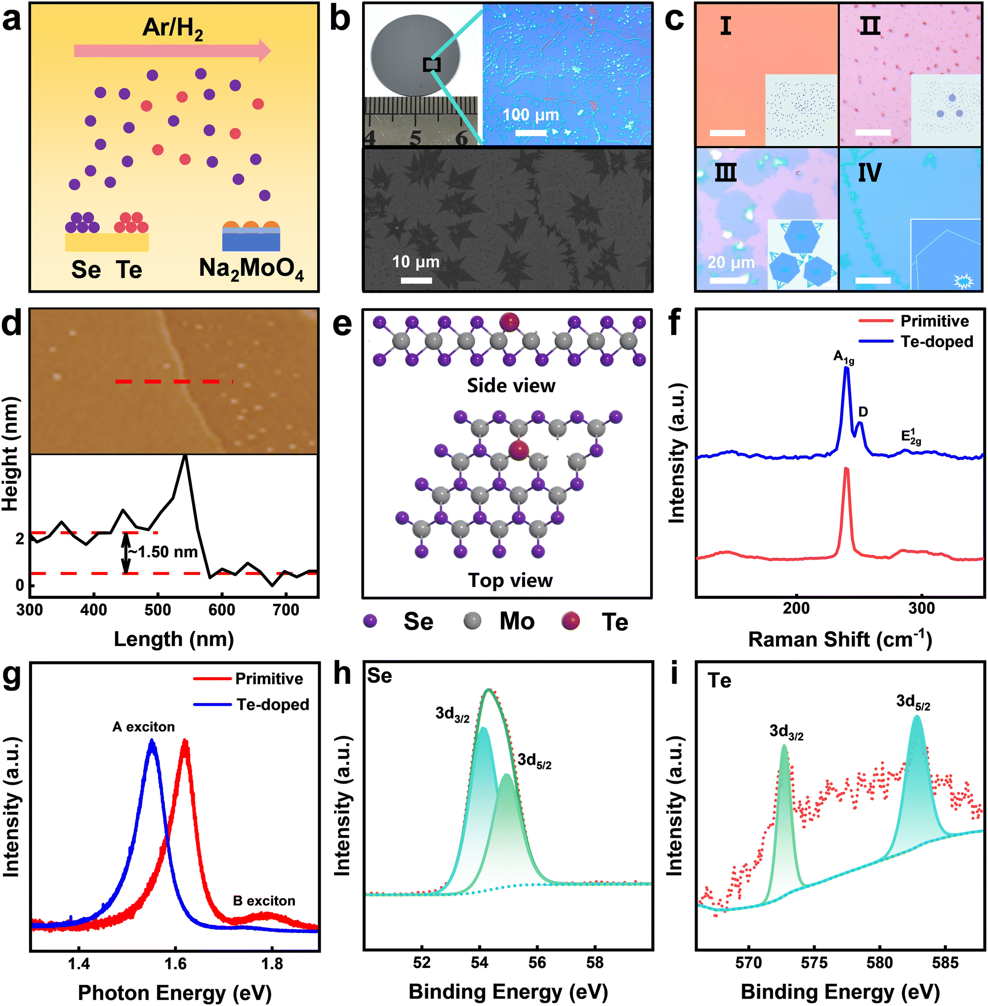 | ||
| Fig. 1 Growth and characterization of CVD-grown Te-doped MoSe2. (a) Flow chart of the general growth process for the production of Te-doped MoSe2 using the CVD method. (b) Upper-left panel: optical image of a Te-doped MoSe2 flake on 1-inch substrate. Upper-right panel: optical microscope image showing the well sealed single crystalline domains. Lower panel: SEM image showing the flat surface with second layer islands. (c) Schematic of the growth process: (I) Homogeneously distributed precursor layer; (II) Annealing-induced precursor concentration gradient formation; (III) Material with insufficient diffusion resulting from short-time growth; (IV) Continuous film formation after sufficient growth duration. (d) AFM image of the Te-doped MoSe2 surface and the height profile along the line over a step edge. (e) Top and side views of ball-stick model of the Te-doped MoSe2 with Se vacancies. (f) Raman and (g) PL spectra of MoSe2 and Te-doped MoSe2 on the SiO2/Si substrate. (h) and (i) XPS spectra of the Se (h) peak and the Te (i) peak of Te-doped MoSe2 on the SiO2/Si substrate. | ||
The growth of wafer-scale Te-doped MoSe2 was achieved by introducing an annealing step prior to the reaction process, enabling the formation of large-area single-domain structures. Fig. 1b presents an optical microscopy image of the resulting Te-doped MoSe2, demonstrating over 95% coverage across the substrate, effectively spanning the entire wafer. Prior to annealing, precursor deposition through spin-coating yielded films limited in size due to the restricted diffusion rate of Mo precursors.33 The precursor distribution has been found to be of crucial importance for the growth of large-area materials.34 When the precursor concentration is relatively high, it tends to favor vertical growth rather than lateral diffusion. This is because the excessive concentration provides an abundance of reactants in the local area, promoting the stacking of layers in the vertical direction, as illustrated in Fig. S2 (ESI†). In contrast, when the precursor concentration is too low, there is a lack of a dominant nucleation center, making it difficult to form large single domains. To facilitate the formation of large single domains, we implemented an annealing step before the reaction.35Fig. 1c illustrates the snapshots in the growth process from the precursor clusters to a continuous film. Initially, precursors were uniformly distributed on the substrate after spin-coating. As shown in Fig. S3 (ESI†), the precursors exhibit uniform distribution, with an atomic force microscope (AFM)-measured root mean square (RMS) roughness of only 5.45 ± 0.5 nm on the spin-coated substrate, further confirming their homogeneous coverage. Then, thermal coalescence facilitated the formation of a favourable precursor concentration gradient, with dominant nucleation centers emerging in the central regions and precursors diffusing outward due to annealing. As this diffusion process occurred, the central nucleation sites absorbed nearby precursor particles, enabling their growth and dominance. Eventually, as these regions expanded, collisions occurred between materials growing from different nucleation centers. As indicated in Fig. S4 (ESI†), AFM images reveal partial protrusions in the edge regions of the sample, while no such features are observed in the central region. This phenomenon supports our hypothesis regarding the diffusion of the precursor. Moreover, surface roughness characterization shows that regions with nucleation centers exhibit an RMS roughness of 1.81 ± 0.3 nm, whereas areas without nucleation centers have a significantly lower RMS roughness of only 0.283 nm, thereby confirming the uniformity of the material surface. To verify the reproducibility of the process, the experiment was repeated 10 times, yielding samples with over 95% coverage in 70% of the trials.
To further validate this observation, we applied a diffusion equation to model the process:36
 | (1) |
To regulate the formation of Se vacancies in MoSe2, Te doping was employed during material growth. As shown in Fig. 1e, the introduction of Te induces lattice distortion in MoSe2 due to its larger atomic radius and different bonding characteristics. Under high reaction temperatures, the Mo–Se bonds become less stable, leading to the partial desorption of Se atoms. This desorption process is thermodynamically favorable as it lowers the overall energy of the system.38,39 To demonstrate the effect of Te doping on the intrinsic properties of MoSe2, we synthesized undoped MoSe2 using Na2MoO4 as the precursor for comparison. We also performed PL and Raman spectroscopy on both undoped and Te-doped samples. Using a 532 nm laser, the Raman spectra of MoSe2 and Te-doped MoSe2 were obtained, as shown in Fig. 1f. The red curve represents the undoped MoSe2 Raman spectrum, where the two prominent peaks correspond to the A1g mode at ∼240 cm−1 and the E12g mode at ∼288 cm−1, indicating the pure 2H phase.
This result confirmed the formation of few-layer MoSe2 crystals. Previous studies on Se-deficient MoSe2 report significant changes in Raman features due to Se vacancies,40 as Se-deficient crystals often display defect-activated phonon peaks. In our Te-doped MoSe2 sample, a slight redshift of approximately 1 cm−1 is observed in the A1g mode, alongside the emergence of a defect-activated phonon peak at 251.6 cm−1, which is attributed to Se vacancies induced by Te doping. Importantly, no new peaks appear in the Raman spectrum, indicating that Te doping preserves the intrinsic characteristics of MoSe2 while introducing Se vacancies. PL spectra further highlight these changes. For undoped MoSe2, as shown in Fig. 1g, the primary peaks are located at 1.57 eV and 1.76 eV, corresponding to A and B excitons,41,42 respectively. It is consistent with prior studies where the strong spin–orbit interaction in MoSe2 leads to distinct exciton emissions. After Te doping, both PL peaks exhibit notable redshifts of 1.50 eV and 1.68 eV, respectively. This shift suggests a narrowing of the bandgap, likely due to the lattice strain and increased Se vacancies introduced by Te, which influence the band structure of MoSe2.43 We further investigated the excitation lifetime of the material using time-resolved photoluminescence (TRPL). As shown in Fig. S7 (ESI†), a bi-exponential decay model yields a fast decay component (τ1 = 0.36 ns) and a slow decay component (τ2 = 4.42 ns). These lifetimes are markedly shorter than those observed for defect-passivated MoSe2,44 suggesting that Te doping introduces additional defects which act as nonradiative recombination centers and thus significantly reduce the overall photoluminescence lifetime. The chemical bonding and composition of the material were characterized through XPS, which confirmed the presence of Mo, Se, and Te in the sample. As shown in Fig. S8 (ESI†), elemental analysis based on peak area integration revealed an atomic ratio of Mo![[thin space (1/6-em)]](https://www.rsc.org/images/entities/char_2009.gif) :Se:Te of 1:1.921:0.055, indicating successful doping of a small amount of Te into the MoSe2 lattice, accompanied by Se vacancies. In the XPS spectra, as shown in Fig. S9 (ESI†), the Mo 3d5/2 and Mo 3d3/2 peaks appear at 229.34 eV and 232.42 eV, suggesting diverse Mo–Se bonding environments. This broadening may be attributed to the inclusion of Te and the formation of Se vacancies. Additionally, as shown in Fig. 1h, the Se 3d peaks are not clearly separated; instead, they form a broad, single peak, further supporting the presence of mixed MoSex compounds. In Fig. 1i, the Te 3d5/2 and Te 3d3/2 peaks observed at 572.68 eV and 583.08 eV confirm the incorporation of Te into the MoSe2 structure, establishing the formation of Te-doped MoSe2. In summary, the introduction of Te during the reaction process altered the crystal structure of MoSe2, facilitating the formation of Se vacancies. Since this defect engineering occurred during material growth, it ensured the uniform doping of Te within the MoSe2 lattice.
:Se:Te of 1:1.921:0.055, indicating successful doping of a small amount of Te into the MoSe2 lattice, accompanied by Se vacancies. In the XPS spectra, as shown in Fig. S9 (ESI†), the Mo 3d5/2 and Mo 3d3/2 peaks appear at 229.34 eV and 232.42 eV, suggesting diverse Mo–Se bonding environments. This broadening may be attributed to the inclusion of Te and the formation of Se vacancies. Additionally, as shown in Fig. 1h, the Se 3d peaks are not clearly separated; instead, they form a broad, single peak, further supporting the presence of mixed MoSex compounds. In Fig. 1i, the Te 3d5/2 and Te 3d3/2 peaks observed at 572.68 eV and 583.08 eV confirm the incorporation of Te into the MoSe2 structure, establishing the formation of Te-doped MoSe2. In summary, the introduction of Te during the reaction process altered the crystal structure of MoSe2, facilitating the formation of Se vacancies. Since this defect engineering occurred during material growth, it ensured the uniform doping of Te within the MoSe2 lattice.
Vacancy-induced trapping states and memory characteristics
In order to verify the trapping effect of defect states on photocarriers, we subsequently designed and fabricated devices on the continuous Te-doped MoSe2 film. The device exhibits an Au–MoSe2–Au configuration. As depicted in Fig. 2a, the device was fabricated under UHV conditions by depositing Au electrodes onto the Te-doped MoSe2 film with a patterned shadow mask. The completed array structure is shown in Fig. S10 (ESI†). To investigate the optoelectronic performance of the devices, photocurrent measurements were conducted in a dark chamber equipped with a high-pressure Xe lamp (λ = 300–1200 nm), a mechanical shutter (>1 ms), and band-pass filters. | ||
| Fig. 2 Configuration and performance of the Te doped MoSe2 device. (a) Schematic view of the synaptic device. (b) I–V curves obtained in the dark (black) and under the illumination of a constant light power intensity (39.7 mW cm−2) with bandpass filters for UV (purple) light. (c) Power-dependent photocurrent of devices as a function of laser intensity. (d) 0.1 V bias I–t curves obtained under shutter-controlled pulse illumination of UV light. (e) I–t curves of primitive MoSe2 (red) and Te-doped-MoSe2 (blue). (f) Schematic model of carrier behavior in Te doped MoSe2. | ||
Based on recent studies, MoSe2 exhibits strong absorption in the UV region.21 To evaluate the photoresponse specifically to UV illumination, a band-pass filter (300–400 nm) was placed in the optical path of the Xe lamp. As shown in Fig. 2b, the purple curve represents the photocurrent under UV illumination, while the black curve denotes the dark current. These results clearly indicate that the device exhibits pronounced sensitivity to UV light. Device-to-device variability and manufacturing reproducibility were evaluated through comparative analysis of optoelectronic characteristics across multiple devices as shown in Fig. S10 and S11 (ESI†), which show highly reproducible photoresponse behaviors.
The I–V curves presented in Fig. S14 (ESI†) were recorded for optical power levels ranging from 3.8 mW cm−2 to 39.7 mW cm−2. The results reveal a large dynamic range of the photoresponse. A linear fitting of the photocurrent (Ip) versus light intensity (P) was performed according to the relationship Ip = cPα, where c is a constant and α is an index associated with the capture and recombination processes of photocarriers.45 The fractional exponent reflects the involvement of trap states in the complex processes of electron–hole generation and recombination within the semiconductor. The logarithmic plot of current versus corresponding light intensity (I–P) in Fig. 2c demonstrates the linear fitting that yields an exponent of α = 0.55. This suggests that the device exhibits a sub-linear photoconductive response, which confirms the trap-mediated photocarrier.46 Additionally, the Te-doped sample exhibits a single pulse of photocurrent upon pulsed illumination, revealing a significantly extended decay time, as shown in Fig. 2d. This extended decay time reflects the memory characteristics of synaptic devices, as carriers are effectively trapped and gradually released due to the trap states introduced by Te doping. To further illustrate the effects of Te doping, Fig. 2e compares the photocurrent response of undoped MoSe2 and Te-doped MoSe2 under the same pulsed UV illumination. The undoped MoSe2 sample exhibits a rapid rise and decay in photocurrent upon light exposure, which indicates fast generation and recombination of electron–hole pairs. In contrast, the Te-doped MoSe2 sample shows a significantly slower rise and decay, reflecting the influence of trap states introduced by Te doping. Similar results have been reported recently in MoS2xSe2(1−x), attributed to the isoelectronic substitution modulated defect levels induced by sulphur vacancies.47 This implies that our defect engineering strategy could apply to other 2D semiconductors.
Specifically, when Te doping induces Se vacancies in MoSe2, defect levels are created near the Fermi energy.48 These defect levels act as traps for photogenerated carriers, imparting non-volatile characteristics to the material.49 As illustrated in Fig. 2f, Te doping introduces localized defect states within the bandgap due to Se vacancies. In the undoped sample, the photoresponse is dominated by the direct generation and recombination of electron–hole pairs.50 However, in the Te-doped sample, electrons are captured by defect-induced trap states (denoted as ET), which temporarily retain photoexcited carriers. This capture process slows down recombination and extends the carrier lifetime. The trap states act as intermediate energy levels that delay carrier relaxation to the valence band, resulting in a prolonged photoresponse.51 This extended photoresponse is particularly beneficial for neuromorphic applications, where slow carrier dynamics can mimic synaptic plasticity, such as memory retention and long-term potentiation.52 By functioning as charge reservoirs, the trap states enable the devices with a memory effect that enhances the device's charge retention and delayed recombination capabilities.53 These characteristics make the Te-doped MoSe2 an excellent candidate for synaptic devices with tunable plasticity.
Synaptic plasticity of Te-doped MoSe2 devices
The investigation of the PPF performance of the Te-doped MoSe2 device is conducted based on its decay time. PPF, a commonly observed manifestation of short-term plasticity (STP) in artificial synapses, occurs when two consecutive optical pulses are delivered in rapid succession. In this process, photocarriers generated by the first pulse become trapped by defect states and are gradually released, leading to their accumulation prior to the arrival of the second pulse. This accumulation results in an enhanced post-synaptic response when the second pulse is applied. As demonstrated in Fig. 3a, when two consecutive UV optical pulses (pulse width: 4 s; interval: 4 s) are applied to the device, the amplitude of the photocurrent evoked by the second pulse (A2) is much higher than that of the first one (A1). This behavior can be estimated by the PPF index defined as | (2) |
 | (3) |
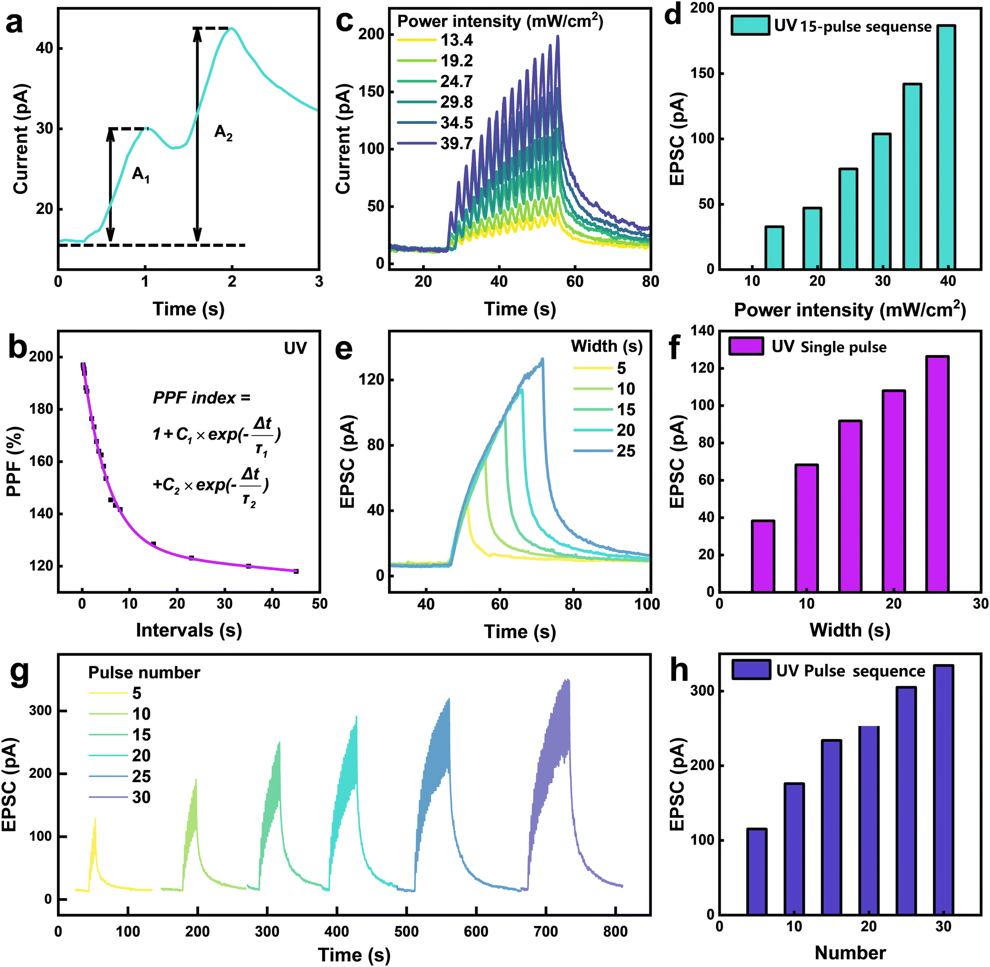 | ||
| Fig. 3 Synaptic plasticity of Te-Doped MoSe2 devices. (a) PPF behavior triggered by two consecutive pulses of UV illumination with a time interval of 0.5 s. (b) PPF index obtained from the input optical pulses with varying spike time interval. (c) Spike-intensity-dependent plasticity of the devices, excitatory post-synaptic current (EPSC) triggered by 15 optical pulses of varying power intensities. (d) ΔEPSC dependency on the pulse power intensities. (e) EPSC under different width variations of the optical pulses. (f) ΔEPSC dependency on the pulse width. (g) Spike-number-dependent plasticity of the devices, EPSC triggered by a set of optical pulses with the quantity ranging from 5 to 30. (h) ΔEPSC dependency on the pulse number. | ||
Since synaptic plasticity is the foundation for the realization of diverse memory functions, the ability to imitate synaptic plasticity is a criterion for evaluating neuromorphic devices.54 The synaptic plasticity of the devices has been systematically investigated under the illumination of shutter-controlled UV pulses. In detail, the excitatory post-synaptic current (EPSC) was measured by applying a series of consecutive optical pulses with varying numbers, frequencies and power intensities, corresponding to verify the SNDP, SRDP and spike-intensity-dependent plasticity (SIDP). Fig. 3c shows the EPSC curves of the device under optical pulses with different intensities. The EPSCs clearly increase with the ascending light intensity, as shown in Fig. 3d. In the biological brain, the learning efficiency also depends on the duration and intensity of learning. Fig. 3e shows the EPSCs under the application of single optical pulses with varying widths. The change of EPSC declines when the width of the optical pulse decreases, and as shown in Fig. 3f, a linear variation in the response is also observed. Fig. 3g shows the EPSCs generated by a stimuli sequence consisting of 5 to 30 UV optical pulses, and the results in Fig. 3h demonstrate the robust SNDP of the devices, as the variation of EPSC (ΔEPSC) increases steadily with the pulse number. An accumulated decay time of the EPSCs can be observed following the end of the pulse sequence, which is similar to the forgetting curve of biological nerves, confirming a long-time memory capability of the artificial synapses, and the alternation of other parameters presents the same result, demonstrating that synaptic plasticity is highly tunable. The time stability of the MoSe2 synaptic device has been evaluated by measuring the SNDP after ambient condition storage for about 3 months, as demonstrated in Fig. S12 (ESI†). The two obtained I–V curves exhibit negligible deviation, confirming that the device is stable in air. The operational durability was further validated through cyclic photocurrent measurements (Fig. S13, ESI†), where the Te-doped MoSe2 synaptic device maintained invariant response characteristics over 200 s illumination cycles. The initial and final photocurrent values showed no statistically significant variation, demonstrating robust operational stability.
Energy consumption is a crucial metric for neuromorphic devices. We calculated the energy consumption per spike using the equation:
| dE = VD × ID × dt | (4) |
Simulation of in-sensor high-pass filtering of images with device parameters
As illustrated in Fig. 4a, the process of memory formation in the brain comprises three critical stages. Sensory memory (SM) is initially generated when external stimuli are received by sensory receptors. This information is then processed into short-term memory (STM), contingent on the level of attention devoted to the stimuli. Subsequently, through repeated exposure or training, STM consolidates into long-term memory (LTM).55 Leveraging the plasticity characteristics of our Te-doped MoSe2 devices, we demonstrate that modulating the number, duration, and intensity of incident optical stimuli can significantly influence EPSCs, thereby facilitating the transition from STM to LTM. This transition underscores the enhanced synaptic plasticity of the device, which enables the retention of optical stimuli over extended durations. The capability of these devices to replicate the learning–forgetting–relearning cycle is further substantiated in Fig. 4b. Specifically, upon the application of ten consecutive optical pulses, the photocurrent exhibited a sustained increase. Following the removal of stimuli, a gradual decrease in photocurrent was observed, indicative of the natural forgetting process. Notably, despite this decline, the current remained elevated relative to its initial state. When subjected to a second training sequence, only four additional pulses were required to restore the current to its initial learned state, mirroring the behavior of biological synapses. | ||
| Fig. 4 The proposed functions of the optoelectronic synaptic device. (a) Scheme of the memory formation process, the information is memorized through the transition from STM to LTM. (b) Simulation of “Learning–experience” behavior, including learning, forgetting, and relearning processes. (c) Spike-rate-dependent plasticity of the devices, EPSC triggered by 10 optical pulses with a duration of 1 s and varying frequency. (d) ΔEPSC dependency on the pulse frequency. (e) The gain of the device, defined as A10/A1, is plotted and fitted as a function of optical pulse frequency. (f) Image of a flower before and after sharpening with the high-pass filter at a cutoff frequency of 0.44 Hz. | ||
In biological systems, synapses with a low initial release probability of neurotransmitters inherently exhibit high-pass filtering properties, where signals above a critical cutoff frequency (fH) are enhanced, and those below are attenuated.56 To evaluate this filtering effect in our Te-doped MoSe2 device, Fig. 4c presents a series of ten optical pulses (350 nm, 39.7 mW cm−2, 1 s) of varying frequencies applied to the device. As shown in Fig. 4d, the EPSC increased from 29 pA to 150 pA as the frequency of optical pulses increased from 0.17 Hz to 5 Hz. The gain of the EPSC response was quantified using the ratio A10/A1, where A10 and A1 denote the amplitudes of the photocurrent triggered by the 10th and the 1st optical pulse, respectively. The dependence of EPSC gain on spike frequency is plotted in Fig. 4e and follows a sigmoidal function:
 | (5) |
The high-pass filtering property of the Te-doped MoSe2 device enables its application in image preprocessing and enhancement. To further illustrate this capability, we simulated the application of a high-pass filter to a raw image with low contrast, as depicted in Fig. 4f. The resulting processed image demonstrates a sharpening effect when filtered at fH, enhancing critical contour features. This phenomenon is intrinsically linked to spike-rate-dependent plasticity (SRDP). In devices where EPSCs exhibit poor frequency-dependent regulation, the correlation between gain and frequency is less pronounced, resulting in an increased fH and consequently diminished filtering efficiency. This property underscores the potential of the Te-doped MoSe2 device in neuromorphic visual processing, where selective enhancement of key features is essential for efficient real-time data processing and artificial vision applications.57
Conclusions
In conclusion, we have reported an ultraviolet-responsive synaptic device array based on wafer-scale Te-doped MoSe2 films. By optimizing the precursor concentration gradient through annealing, we achieved the growth of large-area single-domain MoSe2 films, with domain sizes reaching up to 500 μm. Te doping was introduced during the CVD process to modulate the defect characteristics of MoSe2. Raman and PL analyses confirmed the generation of Se vacancies, while XPS demonstrated that Te doping effectively induced these vacancies. Comparative device performance studies showed a significant improvement in response speed after doping, along with memory effects. This enabled the devices to simulate various synaptic functionalities, including EPSC, PPF, and STP. Additionally, high-pass filtering characteristics were achieved based solely on device parameters, enhancing signal processing and enabling image sharpening, which highlights the potential for integrated sensing and processing applications. This work underscores the importance of defect engineering and high-quality wafer-scale films in achieving reliable neuromorphic device performance, paving the way for applications in next-generation wearable systems and neuromorphic technologies.Experimental
Growth of Te doped MoSe2 samples
Te-doped MoSe2 was grown via a controlled CVD process with a substrate pre-treatment step to enhance precursor–substrate interactions. First, SiO2/Si substrates were treated with oxygen plasma to improve their hydrophilicity. Subsequently, a Na2MoO4 precursor solution was spin-coated onto the substrate at 8000 rpm per minute to form a uniform precursor layer. The CVD process was performed in a dual-zone tube furnace. Equal amounts of Te (150 mg) and Se (150 mg) powders were placed in the heating zone, along with the Na2MoO4-treated substrate. Prior to the reaction, the system was purged with reverse Ar/H2 gas flow (42:8 sccm) while heating the furnace at a rate of 20 °C min−1 to 700 °C. The substrate was then annealed at 700 °C for 10 minutes under the same reverse flow to promote precursor diffusion and uniform nucleation. Following the annealing step, the gas flow was switched to the forward direction, initiating the reaction under the same temperature and flow conditions. The growth process was maintained at 700 °C for 10 minutes before the furnace was allowed to cool naturally to room temperature. This method enabled the successful synthesis of Te-doped MoSe2 films with controlled morphology and composition.
Sample characterization
The sample morphology was characterized using an optical microscope (AOSVI) and an atomic force microscope (Cipher S AFM, OXFORD INSTRUMENTS). The contact angle of the precursor solution droplet on the substrate was measured with a contact angle meter (OCA25, Dataphysics). Photoluminescence spectra were excited using a green light laser with a 532 nm wavelength. The Raman spectra were recorded with a confocal Raman spectrometer (HORIBA) with 532 nm laser excitation. The Si peak at 520 cm−1 was used as a reference for wavenumber calibration. XPS measurements were performed with a dual anode Al/Mg X-ray source on the samples. The energy calibrations were made against the C 1s peak to eliminate the charging of the sample during analysis. The electric transport properties were measured with a dual-channel source meter (Keithley 2636B).Device fabrication
The devices were fabricated within a homebuilt UHV multisource physical vapor deposition system under a pressure of 10−6 Pa. The Au evaporator is degassed, and then evaporation was performed at 1100 °C for 30 minutes. The Au electrodes of 10–100 nm were directly deposited on the sample surface, while the designed patterns were realized using custom-made metal shadow masks.Photoresponse measurements
All the measurements were carried out at room temperature and under ambient air conditions. A high-pressure Xe lamp (CME-SL300, Microenerg) was used as the light source with continuous spectra (wavelength 300–1200 nm). UV results were obtained by placing a band-pass filter (300–400 nm) in the optical path.Author contributions
Y. Pan conceived and supervised the experiments. Y. Hu conducted the sample growth, device fabrication, data collection, analysis, and manuscript drafting with the assistance of all authors. Y. Lin conducted the synaptic performance testing and contributed to the drafting of the corresponding sections. Y. Pan, Y. Lin and Y. Hu validated the results and revised the manuscript.Data availability
Results supporting this article have been included as part of the ESI.† Any other data that support the findings of this study are available from the corresponding authors upon reasonable request.Conflicts of interest
There are no conflicts to declare.Acknowledgements
This work was financially supported by the National Key Research and Development Program of China (Grant no. 2022YFA1204100), the National Natural Science Foundation of China (Grant no. 12074302 and 82200728) and the National Training Program of Innovation and Entrepreneurship for Undergraduates (Grant no. XJ202310698057). We thank the Instrument Analysis Center of Xi’an Jiaotong University for their assistance with PL, Raman, SEM, and AFM measurements. We thank Miss Chenyu Liang at the Instrument Analysis Center of Xi’an Jiaotong University for her assistance with the XPS measurement.Notes and references
- F. Zhou and Y. Chai, Nat. Electron., 2020, 3, 664–671 CrossRef.
- S. Kumar, R. S. Williams and Z. Wang, Nature, 2020, 585, 518–523 CrossRef CAS PubMed.
- V. K. Sangwan and M. C. Hersam, Nat. Nanotechnol., 2020, 15, 517–528 CrossRef CAS.
- L. Yin, W. Huang, R. Xiao, W. Peng, Y. Zhu, Y. Zhang, X. Pi and D. Yang, Nano Lett., 2020, 20, 3378–3387 CrossRef CAS.
- H. L. Park, Y. Lee, N. Kim, D. G. Seo, G. T. Go and T. W. Lee, Adv. Mater., 2020, 32, 1903558 CrossRef CAS PubMed.
- X. Chen, B. Chen, B. Jiang, T. Gao, G. Shang, S. T. Han, C. C. Kuo, V. A. L. Roy and Y. Zhou, Adv. Funct. Mater., 2022, 33, 2208807 CrossRef.
- N. Ilyas, J. Wang, C. Li, D. Li, H. Fu, D. Gu, X. Jiang, F. Liu, Y. Jiang and W. Li, Adv. Funct. Mater., 2021, 32, 2110976 CrossRef.
- Y. Wang, L. Yin, W. Huang, Y. Li, S. Huang, Y. Zhu, D. Yang and X. Pi, Adv. Intell. Syst., 2020, 3, 2000099 CrossRef.
- S. Seo, S.-H. Jo, S. Kim, J. Shim, S. Oh, J.-H. Kim, K. Heo, J.-W. Choi, C. Choi, S. Oh, D. Kuzum, H. S. P. Wong and J.-H. Park, Nat. Commun., 2018, 9, 5106 CrossRef PubMed.
- M. Prezioso, F. Merrikh-Bayat, B. D. Hoskins, G. C. Adam, K. K. Likharev and D. B. Strukov, Nature, 2015, 521, 61–64 CrossRef CAS PubMed.
- R. Jana, S. Ghosh, R. Bhunia and A. Chowdhury, J. Mater. Chem. C, 2024, 12, 5299–5338 RSC.
- K. Liang, R. Wang, B. Huo, H. Ren, D. Li, Y. Wang, Y. Tang, Y. Chen, C. Song, F. Li, B. Ji, H. Wang and B. Zhu, ACS Nano, 2022, 16, 8651–8661 CrossRef CAS PubMed.
- M. M. Islam, A. Krishnaprasad, D. Dev, R. Martinez-Martinez, V. Okonkwo, B. Wu, S. S. Han, T.-S. Bae, H.-S. Chung, J. Touma, Y. Jung and T. Roy, ACS Nano, 2022, 16, 10188–10198 CrossRef CAS.
- J. H. Bong, S. Grebenchuk, K. G. Nikolaev, C. P. T. Chee, K. Yang, S. Chen, D. Baranov, C. R. Woods, D. V. Andreeva and K. S. Novoselov, Nanoscale Horiz., 2024, 9, 863–872 RSC.
- E. Ercan, C.-C. Hung, G.-S. Li, Y.-F. Yang, Y.-C. Lin and W.-C. Chen, Nanoscale Horiz., 2023, 8, 632–640 RSC.
- Q. Chen, J. Cao, Z. Yang, Z. Wang, J. Wang, S. Yu, C. Hao, N. Wang, H. Li and X. Huang, Nanoscale Horiz., 2024, 9, 1023–1029 RSC.
- S. Larentis, B. Fallahazad and E. Tutuc, Appl. Phys. Lett., 2012, 101, 223104 CrossRef.
- J. Xia, X. Huang, L. Z. Liu, M. Wang, L. Wang, B. Huang, D. D. Zhu, J. J. Li, C. Z. Gu and X. M. Meng, Nanoscale, 2014, 6, 8949–8955 RSC.
- J.-L. Meng, T.-Y. Wang, L. Chen, Q.-Q. Sun, H. Zhu, L. Ji, S.-J. Ding, W.-Z. Bao, P. Zhou and D. W. Zhang, Nano Energy, 2021, 83, 105815 CrossRef CAS.
- C. Huang, S. Wu, A. M. Sanchez, J. J. Peters, R. Beanland, J. S. Ross, P. Rivera, W. Yao, D. H. Cobden and X. Xu, Nat. Mater., 2014, 13, 1096–1101 CrossRef CAS PubMed.
- J. Zhong, X. Zhang and G. Xiang, ACS Appl. Mater. Interfaces, 2023, 15, 56049–56056 CrossRef CAS.
- Y. H. Chang, W. Zhang, Y. Zhu, Y. Han, J. Pu, J. K. Chang, W. T. Hsu, J. K. Huang, C. L. Hsu, M. H. Chiu, T. Takenobu, H. Li, C. I. Wu, W. H. Chang, A. T. S. Wee and L. J. Li, ACS Nano, 2014, 8, 8582–8590 CrossRef CAS.
- J. Lee, S. Pak, Y.-W. Lee, Y. Cho, J. Hong, P. Giraud, H. S. Shin, S. M. Morris, J. I. Sohn, S. Cha and J. M. Kim, Nat. Commun., 2017, 8, 14734 CrossRef CAS PubMed.
- H. Yang, Y. Hu, X. Zhang, Y. Ding, S. Wang, Z. Su, Y. Shuai and P. Hu, Adv. Funct. Mater., 2023, 34, 2308149 CrossRef.
- H. K. He, R. Yang, W. Zhou, H. M. Huang, J. Xiong, L. Gan, T. Y. Zhai and X. Guo, Small, 2018, 14, 1800079 CrossRef.
- Z. Hu, Z. Wu, C. Han, J. He, Z. Ni and W. Chen, Chem. Soc. Rev., 2018, 47, 3100–3128 RSC.
- J. Shim, A. Oh, D. H. Kang, S. Oh, S. K. Jang, J. Jeon, M. H. Jeon, M. Kim, C. Choi, J. Lee, S. Lee, G. Y. Yeom, Y. J. Song and J. H. Park, Adv. Mater., 2016, 28, 6985–6992 CrossRef CAS PubMed.
- J. Zhou, J. Lin, H. Sims, C. Jiang, C. Cong, J. A. Brehm, Z. Zhang, L. Niu, Y. Chen, Y. Zhou, Y. Wang, F. Liu, C. Zhu, T. Yu, K. Suenaga, R. Mishra, S. T. Pantelides, Z. G. Zhu, W. Gao, Z. Liu and W. Zhou, Adv. Mater., 2020, 32, 2003123 CrossRef CAS.
- F. Zhou, Z. Zhou, J. Chen, T. H. Choy, J. Wang, N. Zhang, Z. Lin, S. Yu, J. Kang, H. S. P. Wong and Y. Chai, Nat. Nanotechnol., 2019, 14, 776–782 CrossRef CAS.
- X. Xu, T. Guo, H. Kim, M. K. Hota, R. S. Alsaadi, M. Lanza, X. Zhang and H. N. Alshareef, Adv. Mater., 2022, 34, 2108258 CrossRef CAS PubMed.
- L. Zhang, J. Dong and F. Ding, Chem. Rev., 2021, 121, 6321–6372 CrossRef CAS.
- J. Mao, Y. Zhang, Y. Zhang, Y. Lin, Y. Feng, Y. Hu, M. Shafa and Y. Pan, ACS Appl. Mater. Interfaces, 2023, 15, 28267–28276 CrossRef CAS PubMed.
- S. L. Shang, G. Lindwall, Y. Wang, J. M. Redwing, T. Anderson and Z. K. Liu, Nano Lett., 2016, 16, 5742–5750 CrossRef CAS PubMed.
- Z. Xin, X. Zhang, J. Guo, Y. Wu, B. Wang, R. Shi and K. Liu, ACS Nano, 2024, 18, 7391–7401 CrossRef CAS.
- J. Lee and N. Shin, Appl. Phys. Lett., 2023, 123, 181902 CrossRef CAS.
- H. Ye, J. Zhou, D. Er, C. C. Price, Z. Yu, Y. Liu, J. Lowengrub, J. Lou, Z. Liu and V. B. Shenoy, ACS Nano, 2017, 11, 12780–12788 CrossRef CAS PubMed.
- D. Shen, Y. Jin, Z. Zhang, R. Song, M. Liu, W. Li, X. Li, R. Wu, B. Li, J. Li, B. Zhao and X. Duan, Precis. Chem., 2024, 2, 282–299 CrossRef CAS PubMed.
- D. Su, G. Liu, M. Ma, R. Wei, Y. Mu, Z. Yang and G. Zhang, J. Mol. Model., 2024, 30, 29 CrossRef CAS PubMed.
- Y. Zhao, W. Wang, C. Li, Y. Xu and L. He, Solid State Commun., 2018, 281, 6–11 CrossRef CAS.
- M. Mahjouri-Samani, L. Liang, A. Oyedele, Y.-S. Kim, M. Tian, N. Cross, K. Wang, M.-W. Lin, A. Boulesbaa, C. M. Rouleau, A. A. Puretzky, K. Xiao, M. Yoon, G. Eres, G. Duscher, B. G. Sumpter and D. B. Geohegan, Nano Lett., 2016, 16, 5213–5220 CrossRef CAS PubMed.
- X. Lu, M. I. Utama, J. Lin, X. Gong, J. Zhang, Y. Zhao, S. T. Pantelides, J. Wang, Z. Dong, Z. Liu, W. Zhou and Q. Xiong, Nano Lett., 2014, 14, 2419–2425 CrossRef CAS PubMed.
- Z. Tang, S. Luo, G. Guo, X. Huang, Y. Peng, X. Tang, Q. Chen, X. Qi and J. Zhong, Phys. Status Solidi B, 2024, 261, 2400185 CrossRef CAS.
- S. Zhao, M. Lu, S. Xue, L. Tao, Y. Sui and Y. Wang, Appl. Phys. Lett., 2019, 115, 063105 CrossRef.
- A. O. A. Tanoh, J. Alexander-Webber, Y. Fan, N. Gauriot, J. Xiao, R. Pandya, Z. Li, S. Hofmann and A. Rao, Nanoscale Adv., 2021, 3, 4216–4225 RSC.
- H. Kind, H. Yan, B. Messer, M. Law and P. Yang, Adv. Mater., 2002, 14, 158–160 CrossRef CAS.
- M. M. Furchi, D. K. Polyushkin, A. Pospischil and T. Mueller, Nano Lett., 2014, 14, 6165–6170 CrossRef CAS PubMed.
- L. Yin, P. He, R. Cheng, F. Wang, F. Wang, Z. Wang, Y. Wen and J. He, Nat. Commun., 2019, 10, 4133 CrossRef.
- Z. Xu, C. Liu, C. Sun, S. Zhao, Q. Yuan and Z. Chen, Phys. B, 2024, 675, 415643 CrossRef CAS.
- J. Jiang, P. Yang, J. J. Liou, W. Liao and Y. Chai, Nano Res., 2022, 16, 3104–3124 CrossRef.
- Y.-H. Chang, W. Zhang, Y. Zhu, Y. Han, J. Pu, J.-K. Chang, W.-T. Hsu, J.-K. Huang, C.-L. Hsu, M.-H. Chiu, T. Takenobu, H. Li, C.-I. Wu, W.-H. Chang, A. T. S. Wee and L.-J. Li, ACS Nano, 2014, 8, 8582–8590 CrossRef CAS.
- X. Ren, X. He, X. Li, Y. Li, F. Gao, J. Zhang and P. Hu, Adv. Opt. Mater., 2024, 12, 2302852 CrossRef CAS.
- X. Yan, Q. Zhao, A. P. Chen, J. Zhao, Z. Zhou, J. Wang, H. Wang, L. Zhang, X. Li, Z. Xiao, K. Wang, C. Qin, G. Wang, Y. Pei, H. Li, D. Ren, J. Chen and Q. Liu, Small, 2019, 15, 1901423 CrossRef PubMed.
- X. Wang, Y. Zong, D. Liu, J. Yang and Z. Wei, Adv. Funct. Mater., 2023, 33, 2213894 CrossRef CAS.
- S. T. Keene, C. Lubrano, S. Kazemzadeh, A. Melianas, Y. Tuchman, G. Polino, P. Scognamiglio, L. Cina, A. Salleo, Y. van de Burgt and F. Santoro, Nat. Mater., 2020, 19, 969–973 CrossRef CAS PubMed.
- B. Das, S. Baek, J. Niu, C. Jang, Y. Lee and S. Lee, ACS Nano, 2023, 17, 21297–21306 CrossRef PubMed.
- X. Miao, Y. Zhang, Y. Lin, H. Lei, T. Min and Y. Pan, Adv. Opt. Mater., 2024, 12, 2400358 CrossRef CAS.
- J. Wang, B. Yang, S. Dai, P. Guo, Y. Gao, L. Li, Z. Guo, J. Zhang, J. Zhang and J. Huang, Adv. Mater. Technol., 2023, 8, 2300449 CrossRef CAS.
Footnotes |
| † Electronic supplementary information (ESI) available. See DOI: https://doi.org/10.1039/d5nh00062a |
| ‡ These authors contributed equally to this work. |
| This journal is © The Royal Society of Chemistry 2025 |