
 Open Access Article
 This Open Access Article is licensed under a
 Creative Commons Attribution 3.0 Unported Licence
Self-assembly of isolated plasmonic dimers with sub-5 nm gaps on a metallic mirror†
Vasanthan
Devaraj
 *ab,
Isaac Azahel Ruiz
Alvarado
c,
Jong-Min
Lee
d,
Jin-Woo
Oh
*e,
Uwe
Gerstmann
c,
Wolf Gero
Schmidt
c and
Thomas
Zentgraf
*ab
*ab,
Isaac Azahel Ruiz
Alvarado
c,
Jong-Min
Lee
d,
Jin-Woo
Oh
*e,
Uwe
Gerstmann
c,
Wolf Gero
Schmidt
c and
Thomas
Zentgraf
*ab
aDepartment of Physics, Paderborn University, 33098 Paderborn, Germany. E-mail: vasanthan.devaraj@uni-paderborn.de; thomas.zentgraf@uni-paderborn.de
bInstitute for Photonic Quantum Systems (PhoQS), Paderborn University, 33098 Paderborn, Germany
cTheoretical Materials Physics, Paderborn University, 33098 Paderborn, Germany
dSchool of Nano Convergence Technology & Nano Convergence Technology Center, Hallym University, 24252 Chuncheon, Republic of Korea
eBio-IT Fusion Technology Research Institute, Pusan National University, 46241 Busan, Republic of Korea. E-mail: ojw@pusan.ac.kr
First published on 10th December 2024
Abstract
Realizing plasmonic nanogaps with a refractive index (n = 1) environment in metallic nanoparticle (NP) structures is highly attractive for a wide range of applications. So far in self-assembly-based approaches, without surface functionalization of metallic NPs, achieving such extremely small nanogaps is challenging. Surface functionalization introduces changes in the refractive index at nanogaps, which in turn deteriorates the desired plasmonic properties. In addition, fabrication of low-density dimer NP designs with smaller nanogaps poses a big challenge. Here, we introduce a simple and straightforward self-assembly-based strategy for the fabrication of low-density, isolated dimer gold nanoparticles in a nano-particle-on-metallic-mirror (NPoM) platform. A minimum interparticle gap distance between NPs of ∼3 nm is achieved without surface functionalization. This is possible by utilizing the M13 bacteriophage as the spacer layer instead of SiO2 in NPoM. Density functional theory calculations on Au atom adsorption on SiO2 and M13 bacteriophage surface constituents trace the NP assembly on the latter to a comparatively weak interaction with the substrate. Our study offers an attractive route for fabricating low density plasmonic dimer structures featuring small nanogaps and will enrich structure specific/isolated studies benefitting a variety of optical, actuator, and sensing applications.
New conceptsIn this work, we introduce a simple, cost-effective, self-assembly approach to fabricate low-density dimer nanoparticles (NPs) in a nanoparticle-on-metallic-mirror (NPoM) architecture, achieving interparticle gap distances as small as ∼3 nm. Utilizing the M13 phage as a spacer layer, we avoided the need for metallic surface functionalization, one of the common strategies often employed to fabricate dimers. DFT calculations provide new insights into why the use of SiO2 hinders dimer formation, revealing the formation of strong Au–Si bonds that restrict NP mobility, unlike the weakly bonded structures on the M13 phage. This approach offers significant potential for creating tunable and dynamic plasmonic devices. Due to humidity, a dynamic change in the M13 phage film's thickness produces a plasmonic scattering peak shift, with full reversibility. These findings extend the versatility of plasmonic nanogaps for applications in sensors, dynamic optical devices, and emitter interactions, advancing the field beyond current fabrication techniques. |
Introduction
Plasmonic nanostructures have attracted much attention owing to their extreme light confinement at the nanoscale, allowing the manipulation of light below the diffraction limit.1–3 This capability of plasmonic nanostructures allowed them to be developed for highly efficient applications in multidisciplinary fields spanning physics, chemistry, and life sciences.4–12 In particular, three strategies are commonly employed to control the plasmonic properties by the distance, dielectric environment, and carrier doping.2 Out of these, distance control is one potential method to achieve superior plasmonic properties. By controlling the distance between metallic nanoparticles (NPs), it is possible to modify the localized surface plasmon resonance (LSPR) wavelength, large near-field strength within the nanogap, hybridization of plasmonic modes, emitter interactions at the nanocavity, plasmon dephasing process, and so on.13–17Dimer NPs positioned on a dielectric film/metallic mirror substrate or so-called nanoparticle-on-mirror (NPoM) designs is one of the good candidates to demonstrate the abovementioned properties.18–22 So far, specific distance control between dimer NPs23–25 have been obtained either with lithographical assistance12,26–28 or by metallic surface functionalization like DNA mediated self-assembly,29–36 programmable molecular assembly,37 support via ligands or polymers,38,39 electrostatic self-assembly,40–42 and few others.43–45 However, the surface functionalization of metallic nanoparticles introduces changes in the refractive index (with n ≠ 1) in particular if it occurs close to the nano-gap (interparticle distance or hot-spot), which in turn deteriorates the plasmonic properties. Without these assistances, when metallic NPs are deposited on top of a substrate (for example SiO2), aggregated nanostructures may form.46,47
Often this aggregation hinders the investigation of structure specific optical interactions. For example, in densely assembled NPs on a substrate, the contribution of optical properties (for example, near-field enhancement and LSPR resonance) comes from the sum of closely self-assembled multiple nanoparticles (Fig. 1a). The questions will be whether and how we can extract optical results from an isolated structure specific interaction (for example, dimer NPoM only), independently? One good strategy is to test with a low density of metallic NPs without involving any surface functionalization. Considering these factors, the necessity to develop a self-assembly strategy (without involving lithographical assistance) to fabricate a dimer NP in NPoM architectures without hindering a hot-spot environment (refractive index) will be highly advantageous for numerous applications. Furthermore, achieving a multitude of tunable plasmonic properties from a single plasmonic design will be significantly attractive.
 | ||
| Fig. 1 Schematic illustration of (a) dense aggregation of metallic nanoparticles on top of a spacer layer/metallic mirror substrate. (b) Self-assembly of low-density dimer nanoparticles with clear isolation from each other on top of a spacer layer/metallic mirror substrate without any lithography based assistance or surface functionalization, which is the focus of this work. | ||
In this work, we show such merit-design by introducing a simple self-assembly fabrication approach without involving any surface modifications or lithographical assistance to fabricate dimer NPoMs (hereafter d-NPoMs). We aim to achieve fabrication of low-density NPs on a substrate through a self-assembly approach with a clear spatial isolation of dimer metallic NPs (Fig. 1b). This is possible by replacing the traditional SiO2 with a biomaterial (M13 bacteriophage or M13 phage) thin film. An advantage of using the M13 phage is that it is not only limited to plasmonics but also extends to applications such as biosensors and actuators, due to its selectivity enabled by genetic engineering and its broad range of activation possibilities.48–51 Under similar fabrication conditions, we analyzed the formation of d-NPoMs on SiO2versus the M13 phage. Using density functional theory (DFT) simulations, we investigate how the M13 phage biofilm acts as an excellent template in achieving self-assembly of low-density dimers as opposed to SiO2. We successfully tested the reproducibility of achieving such low-density d-NPoMs. Plasmonic scattering properties of d-NPoMs with varied thickness of the M13 phage layer are investigated. Finally, we demonstrate the dynamic properties of d-NPoMs involving the M13 phage, where it is possible to modify the wide range of LSPR resonances from a single structure. We believe that developing such low-density d-NPoMs will help in enhancing design specific studies for precisely understanding a multitude of optical properties.
Experimental and methods section
Simulations
Optical simulations are carried out using a three-dimensional electromagnetic solver based upon the finite-difference time-domain method (Lumerical FDTD, ANSYS Optics).22,52,53 A plane-wave broadband light source is used to excite the plasmonic nanostructure in a normal direction from the top. Perfectly matched layer boundary conditions are employed in XYZ directions. A box-shaped monitor is positioned close to the NPoM nanostructures to extract the scattering spectra. 3D surface charge density distribution mappings are calculated by considering the following factors: outward normal vector, local electric field, and skin effect.17,22 A mesh size of 5 nm is generally employed in our model with a mesh over-ride size of 0.5 nm surrounding the NPoM structure. The refractive indices used in the model are as follows: Johnson and Christy (Au), Palik (SiO2) and n = 1.37 for the M13 phage.49,51,54,55Density-functional theory (DFT) calculations are performed using the Vienna Ab-initio Simulation Package (VASP).56 The electron exchange correlation is treated within the generalized gradient approximation (GGA) using the PBE functional.57 The electron–ion interactions are within the projector-augmented wave (PAW) scheme.58,59 The van der Waals interactions are accounted for by Grimme's DFT-D approach60 with the Becke–Johnson damping function.61 The electron wavefunctions are expanded in a plane wave basis up to a cut-off energy of 550 eV. All structures are relaxed until the total forces are lower than 0.02 eV Å−1. A dipole correction62 is used to reduce spurious electric fields arising from the periodic boundary conditions due to the non-equivalent slab surfaces.
Fabrication of plasmonic NPoMs
Gold coated Si substrates are utilized for SiO2 and M13 phage based NPoM structures. A 100 nm thick gold film is deposited on Si using an e-beam evaporator. SiO2 is deposited on the Au/Si substrates using a plasma-enhanced chemical vapor deposition (PECVD) method at 350 °C. Au NPs of 75 nm size (NanoComposix, 1 mg mL−1) are then spin-coated on a SiO2/Au/Si substrate. For the NPoMs involving the M13 phage as the spacer layer, a spin coating strategy is utilized. Initially, wild type M13 phage suspensions are prepared by dispersing the phages in a buffer solution made up of Tris-buffered saline (12.5 mM of Tris and 37.5 mM of NaCl, pH 7.5). The concentrations of the M13 phage solutions are then estimated through an ultraviolet-visible spectrometer (EVO300PC, Thermo Scientific), and a Beer–Lambert law calculation. To deposit different thicknesses of M13 phage film, the spin-coating method (1500 rpm, 120 seconds) is employed. By modifying the concentration (3 mg mL−1, 4 mg mL−1, 5 mg mL−1, and 6 mg mL−1) of M13 phage solutions, it is possible to deposit nanometer-thick biofilms in the range of 10 nm, 20 nm, 30 nm, and 40 nm, respectively. Au NPs (1 mg mL−1) are then spin-coated on M13 phage/Au mirror to form low-density dimer NPs. Scanning electron microscopy (SEM) measurements were taken using an S-4800 scanning electron microscope (Hitachi).Atomic force microscopy
The height profiles of M13 phage biofilms are measured using an NX10 AFM (Park Systems) in non-contact mode and XEP 3.0.4 data acquisition software. The AFM images are then postprocessed using the XEI 1.8.2 image program (Park Systems). We used an PPP-NCR specialized probe for non-contact measurements (Nanosensors).Optical characterizations
Plasmonic measurements of NPoMs are carried out using a bright field (BF)/dark field (DF) microscope (Olympus BX53M). The nanostructures are illuminated with an unpolarized halogen lamp source and scattering light is recorded from the sample using a 100× (0.9 NA) objective lens in DF mode. The fiber optic spectrometer (US/USB4000, Ocean Optics) connected to the microscope is used to measure the scattering spectra via SpectraSuite software. A home-built humidity chamber with a controlled moisture flow inlet monitored by the humidity sensor is designed to conduct dynamic optical measurements. Initially, any presence of moisture inside the chamber is removed by passing dry N2 gas and confirmed with a humidity level sensor. Variation of relative humidity levels (RH 20% to 90%) in an increment of 10% is carried out to measure the dynamic plasmonic scattering spectra.Results and discussion
Why we need a dimer NPoM architecture?
Fig. 2 shows the plasmonic properties of a single NPoM (s-NPoM) and a dimer NPoM (d-NPoM) architecture. A schematic of a s-NPOM design (Fig. 2a) and its corresponding plasmonic scattering results (simulated) in Fig. 2(b and c) as a function of spacer layer thickness “t” is shown. The tunability of a localized surface plasmon resonance (LSPR) wavelength is highly sensitive to “t” as shown from these results. From t = 2 nm to 6 nm, the resonant scattering wavelength is shifted from 578 nm to 550 nm. For t > 6 nm, we find that there are negligible or no peak scattering wavelength shifts as we increase the thickness of the spacer layer. To understand the underlying optical differences, we can split these plasmonic scattering properties into two regions (Fig. 2c): the green color shaded region displaying the presence of a strong gap-plasmonic coupling or gap-mode (GM) in the nanocavity region of the s-NPoM structure; the light yellow color shaded region displaying weak scattering properties due to the absence of the GM. This is also reflected in a near-field enhancement |E/E0| (see Fig. S1a, ESI†). Single-NPoMs are well known for their strong gap plasmonic coupling, high quality factor, Purcell enhancement, and the ability to confine photons to deep sub-wavelength scales.63–65 However, these effects are only achievable with an extremely thin spacer layer, particularly in the case of spherical nanoparticles (NPs). The two main concerns in integrating a s-NPOM in a variety of applications will be as follows: (i) high sensitivity to “t” with availability of the GM only until 6 nm of spacer layer thickness;22,52 (ii) difficulties in achieving highly efficient designs or devices (ex. optical nanostructures, sensing devices). The latter problem is critical due to the size limitations of biomaterials or quantum dots (∼>6 nm or above), when integrated with s-NPoM architectures, realizing highly efficient application(s) will be difficult. | ||
| Fig. 2 (a) Cross-sectional illustration of a single NPoM (s-NPoM) design. (b) Simulated plasmonic scattering results from s-NPOM as a function of spacer layer thickness “t”. (c) Deterioration of gap mode (GM) as a function of spacer layer thickness “t” in s-NPoM. (d) Cross-sectional illustration of a dimer NPoM (d-NPoM) design. (e) Simulated plasmonic scattering results from d-NPOM as function of spacer layer thickness “t”. (f) Displaying better plasmonic properties from d-NPOM in terms of availing GM at a larger spacer layer thickness (purple color shaded region) as compared with a t = 2 nm s-NPoM architecture (dashed line). | ||
Nanoparticles with a large facet area facing the bottom mirror surface show a stable gap mode even when the spacer layer is thicker than 6 nm. A representative example of this system is the nanocube-based NPoM.53 However, it is difficult and costly to synthesize nanoparticles with wide facets (single bottom faceted spherical NP).22,53 Another solution to increase the bottom facet is to use dimer NPs on a metallic mirror platform (d-NPoM). Fig. 2d shows a schematic of a d-NPoM design and the corresponding simulated scattering results in Fig. 2e. In this model, we fixed the distance “g” between two NPs as 3 nm and varied the spacer layer thickness “t”. As our focus is to integrate biomaterials and quantum dots (as few examples) with NPoM to realize a variety of applications, we set the minimal “t” as 10 nm (or in other words at larger spacer layer thickness). It is interesting to see even when “t” is varied from 10 nm to 40 nm, continuous tunability in scattering peak wavelengths is observed. To signify the critical advantage of the d-NPoM design, its peak scattering wavelength shift as a function of “t” has been plotted and these results are compared with a s-NPoM design having t = 2 nm (Fig. 2f). As a comparison we plot the scattered resonance peak of a s-NPoM structure (dotted line in the light grey shaded elliptical region) with t = 2 nm. The peak scattering wavelengths continuously shifted from 641 nm to 610 nm when “t” increased from 10 nm to 40 nm for the d-NPoM displaying much better plasmonic performance than the s-NPoM. This continuous shift is only possible due to the presence of the GM throughout this varied spacer layer thickness. In addition to these scattering properties, d-NPoM at t = 10 nm and t = 40 nm displayed ∼150% and ∼125% times better near-field enhancement |E/E0| performance as compared with the s-NPoM design with t = 2 nm spacer layer thickness (see Fig. S1b, ESI†). Good scattering peak wavelength shift and better near-field enhancement |E/E0| properties showcase the importance of utilizing d-NPoM design, especially when we need to incorporate external materials (ex. biomaterial, quantum dots, 2D material etc.) into the NPoM design.
To understand the nature of the plasmonic properties between s-NPoM and d-NPoM, we plot cross-sectional electric field profiles and the corresponding three-dimensional surface charge density distribution mappings (Fig. 3). As we see from the s-NPoM design (Fig. 3a), a large near-field enhancement is observed at the cavity region between the NP and the surface mirror for t = 2 nm. As the spacing “t” increases further, this near-field enhancement surrounding the cavity region starts to deteriorate (ex. until t = ∼6 nm). For t ≥ 10 nm, the near field enhancement at the cavity region becomes negligible. To extract the plasmonic modes originating from these structures as a function of “t”, three-dimensional surface charge density distribution mappings (Fig. 3b) serve as an effective method. For t = 2 nm and 6 nm, the bright dipole mode originates from strong gap-plasmonic coupling (as the contribution comes from the cavity region), hence terming it as a gap mode. For t ≥ 10 nm, in spite of being in the dipole mode, as its origin arises from a NP mode, it has negligible contribution to the peak scattering wavelength shift or near field enhancement. Now, moving to d-NPoM, two cavity regions are available: (i) one as we see from s-NPoM's cavity (NP – dielectric/metallic film region), and (ii) the second one is the cavity region (g) between two NPs in air. Due to the combination of these two cavities, better near-field enhancement can be seen from the cross-sectional electric field profiles (Fig. 3c). The field intensity nature between two NPs at the “g” region remains ∼ consistent (as “g” was fixed).
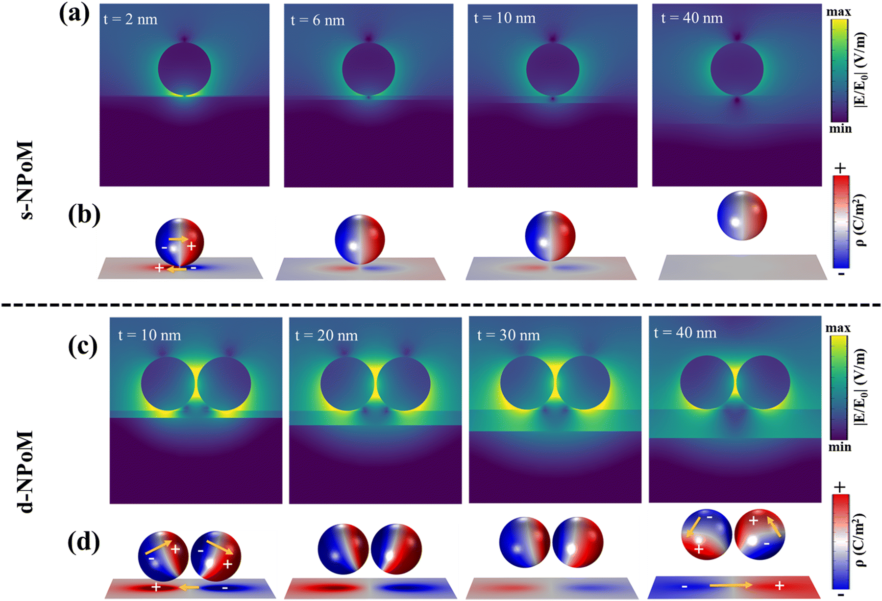 | ||
| Fig. 3 Simulated cross-sectional XZ electric field amplitude profiles (a) and corresponding 3D surface charge density distribution mappings (b) for a s-NPoM structure with a spacer layer thickness of t = 2 nm, 6 nm, 10 nm, and 40 nm. Simulated cross-sectional XZ electric field amplitude profiles (c) and corresponding 3D surface charge density distribution mappings (d) for a d-NPoM structure with a spacer layer thickness of t = 10 nm, 20 nm, 30 nm, and 40 nm. | ||
On the other hand, |E/E0| is deteriorating at the NP-dielectric-metallic film region when “t” increases from 10 nm to 40 nm, but still showcases higher field enhancement than the s-NPoM. At a thickness of t = 10 nm, the near field coupling between the NP and the metallic mirror occurs in a straight perpendicular direction (indicated by a dotted black line, Fig. S2a (ESI†), t = 10 nm). Additionally, a variation in field intensity is observed within the inner region between the two NPs on the top spacer layer (highlighted by the dotted white ellipse, Fig. S2a (ESI†), t = 10 nm). As the thickness increases to t = 40 nm, the near-fields oriented towards the metallic mirror deviate from the initial perpendicular orientation (refer to the dotted black line, Fig. S2a (ESI†), t = 40 nm). Despite this deviation, the gap-plasmonic coupling remains intact. Concurrently, due to the deviation in the near-field orientation, the field strength within the region between the two NPs on the top spacer layer decreases (indicated by the dotted white ellipse, Fig. S2a (ESI†), t = 40 nm). These overall changes in the near field coupling between the NP and the metallic mirror result in a rotation of the surface charge positions, as illustrated by the three-dimensional surface charge density distribution maps (Fig. 3d and Fig. S2b, ESI†). Despite this shift in charge position, the dipolar mode within the NPs is still preserved. The important point to note here is that the origin of all these dipolar modes always arises from the gap-plasmonic coupling. This shows the critical advantage of the d-NPoM design where we can achieve the plasmonic GM even with large spacer layer thickness (10 nm to 40 nm) as compared with s-NPOM where there are no GM at similar “t”. With d-NPoMs, we can achieve continuous scattering resonance tunability up to t = 40![[thin space (1/6-em)]](https://www.rsc.org/images/entities/char_2009.gif) nm, while maintaining the gap-plasmonic mode (brighter dipolar mode). This is not the case with s-NPoMs, where tunability is extremely limited to t ≈ 6nm. Additionally, as a reference, we simulated dimer NPs on a spacer layer without a metallic mirror to compare their properties with d-NPoMs (Fig. S3, ESI†). While it is possible to tune the peak scattering resonances (Fig. S3b, ESI†) by varying the interparticle distance g, the near-field enhancement is consistently superior when a metallic mirror is introduced (Fig. S3c, ESI†). Under our fabrication conditions, tuning the M13 phage layer thickness is more feasible than modifying the interparticle distance between NPs, as shown in Fig. S3 (ESI†). Overall, our d-NPoMs offer simple and straightforward fabrication steps while maintaining low costs. Hence, the d-NPoMs can serve as an alternative candidate in obtaining robust field enhancement, especially when focusing on larger “t”-based NPoM designs with the availability of plasmonic GMs.
nm, while maintaining the gap-plasmonic mode (brighter dipolar mode). This is not the case with s-NPoMs, where tunability is extremely limited to t ≈ 6nm. Additionally, as a reference, we simulated dimer NPs on a spacer layer without a metallic mirror to compare their properties with d-NPoMs (Fig. S3, ESI†). While it is possible to tune the peak scattering resonances (Fig. S3b, ESI†) by varying the interparticle distance g, the near-field enhancement is consistently superior when a metallic mirror is introduced (Fig. S3c, ESI†). Under our fabrication conditions, tuning the M13 phage layer thickness is more feasible than modifying the interparticle distance between NPs, as shown in Fig. S3 (ESI†). Overall, our d-NPoMs offer simple and straightforward fabrication steps while maintaining low costs. Hence, the d-NPoMs can serve as an alternative candidate in obtaining robust field enhancement, especially when focusing on larger “t”-based NPoM designs with the availability of plasmonic GMs.
Fabrication of low-density dimer architectures
At first, we utilized SiO2, a commonly employed spacer layer material in plasmonic studies, as reported in numerous literature studies (Fig. 4a). The Au NPs are spin coated on the SiO2 substrate with the specific goal of achieving a low density of Au NPs. Fig. 4b and c show scanning electron microscopy (SEM) images with two different resolutions (large area and small area), obtained from the SiO2 substrate. s-NPoMs are formed clearly in most circumstances, and the self-assembly of d-NPoMs is not seen. We repeated the fabrication several times and obtained the same results. In rare cases we observed an aggregation of NPs (see Fig. S4, ESI†). Although there are instances where d-NPoMs (Fig. 4b, blue dashed circle) are formed, but considering a scenario for large area fabrication, their ratio is negligible when compared with the formation of s-NPoMs (>95%). The question now remains: how can we reduce the formation of single NPs and thereby improve the ratio of dimer NPs at low density. | ||
| Fig. 4 (a) Fabrication approach with SiO2/Au films to fabricate low density plasmonic NPoMs. (b) and (c) Scanning electron microscopy (SEM) images taken at two different magnifications of spin coated Au NPs on top of SiO2/Au films revealing the presence of s-NPoMs mostly. (d) Fabrication approach with M13 phage/Au films to fabricate low density plasmonic NPoMs. (e) and (f) SEM images taken at two different magnifications of spin coated Au NPs on top of a biomaterial coated Au mirror revealing successful self-assembly of low-density d-NPoMs. (g) Fabrication conditions are repeated to confirm the 100% reproducibility of low-density d-NPoMs when using the M13 phage as a spacer layer. Scale bar is 200 nm. (h) SEM image randomly taken of our sample revealing that it is also possible to obtain only d-NPoMs without involving any single NP. (i) High-resolution SEM image of a d-NPoM, displaying the self-assembly of dimer NPs with a smaller interparticle gap distance. | ||
In our next step, we replaced SiO2 with a biomaterial called the M13 bacteriophage (or hereafter M13 phage). The M13 phage is nanofibrous in nature with a diameter of ∼6.6 nm, a height of ∼880 nm, and a refractive index similar to that of a dielectric material (Fig. 5a). The surface of the M13 phage is densely packed with 2700 copies of perfectly identical functional peptides, and the sequence of these peptides can be freely controlled through genetic engineering.48–51 Utilizing the same fabrication conditions as employed with SiO2, we spin-coated the Au NPs onto the M13 phage substrate (Fig. 4d). Fig. 4e and f show SEM images taken from this substrate, displaying successful self-assembly of low-density d-NPoMs (yellow dashed circles), which are clearly separated from each other. Even though we also see single NPs, the dimer NPs are formed successfully at ∼50% of the area (based upon NP counts). To confirm the formation of d-NPoMs and ensure reproducibility, we repeated the fabrication process twice over the span of approximately one month, producing 10 samples in each set. Consistently, self-assembled low-density dimer architectures were obtained, confirming reproducibility (Fig. 4g and see also Fig. S5 and S6, ESI†). The spin-coating parameters play a crucial role in fabricating d-NPoMs. All fabrications were carried out at room temperature. In some cases, extremely low-density d-NPoMs can also be achieved, showcasing the advantage of our fabrication utilizing the M13 phage as a template (Fig. 4h and i). In certain areas of our sample, we observed the formation of higher-order NP aggregates; however, their occurrence is extremely rare compared to the dimer assemblies (Fig. S5(d, h, and i), S6 and S7, ESI†). It is evident that the M13 phage serves as an excellent template in the fabrication of low-density d-NPoMs which are isolated from each other as compared to SiO2.
 | ||
| Fig. 5 (a) Geometrical information of M13 phages with glutamic acid (E) – glycine (G) – aspartic acid (D) being the main pVIII wild type genome sequence utilized in this work. Density functional theory calculations. (b)–(e) Stable configuration for Au adsorbed on E, G, D, and SiO2 respectively. (f)–(h) Stable configurations resulting from Au–H displacement reactions with E, G, and SiO2, respectively. No stable configuration was found in the case of D. Atom color descriptions: red (O), yellow (Au), brown (C), beige (H), light blue (N), and blue (Si). (i) Energies of Au adsorption configurations (b)–(h) calculated with respect to the Au bulk reservoir and molecular hydrogen. The lower the value, the more stable the configuration. | ||
Why does the M13 phage act as a good template for self-assembling dimer NPoMs?
It is essential to understand why the M13 phage helps in fabricating successful d-NPoMs, and why SiO2 does not. To rationalize the surprising finding that Au nanoparticles tend to aggregate on M13 phages in contrast to SiO2 surfaces, density-functional theory (DFT) calculations on model systems were performed (Fig. 5). Specifically, the adsorption of single Au atoms on the M13 phage constituents glutamic acid (E), glycine (G) and aspartic acid (D) was calculated. This EGD serves as a main pVIII genome sequence of the wild-type M13 phage that we employed for this work (Fig. 5a). We probed all plausible adsorption sites and additionally allowed for the possibility of displacement reactions, where hydrogen desorbs upon bond formation with Au. To be able to compare the structures with different stoichiometries energetically, we assume an Au chemical potential corresponding to bulk Au and a hydrogen chemical potential that equals H2. It turns out that in the case of Au bonding to the M13 phage constituents, the attachment to nitrogen is most favourable (Fig. 5b–d). Amorphous silicon dioxide (a-SiO2) was modelled by the structure proposed in ref. 66. Gold adsorption on a-SiO2 was calculated by sampling a dense mesh of surface bonding sites. Again, we allowed for H displacement reactions, where hydrogen is released upon Au bonding to a-SiO2. The calculations show that Au attachment to saturated glutamic acid, glycine, aspartic acid, and amorphous silicon dioxide leads to roughly similar adsorption energies that vary by at most 0.5 eV. The situation changes, however, as soon as H displacement reactions are allowed for. While in the case of glutamic acid and glycine a moderate energy increase (of the order of 0.1 eV) or decrease (by about 0.5 eV), respectively, is observed, and no stable configuration could be found for aspartic acid. The most prominent energy change, however, occurs for a-SiO2. In that case, hydrogen displacement allows for the formation of energetically very favorable Si–Au bonds. Thus, Au adsorption on a-SiO2 leads to a very stable configuration. In fact, the Au@a-SiO2 structure in Fig. 5h is the far most stable configuration identified in the present study. It is by 0.8…1.4 eV more stable than any other structures identified here. Obviously, Au bonds less strongly to the M13 phage material than to silicon dioxide. Consequently, the diffusion barriers are lower and the diffusivity higher on the M13 phage than on a-SiO2. Therefore, we expect a comparatively high mobility of Au NP on M13 phages. Substrate mediated, long range strain and Coulomb interactions between the clusters,67–69 as well as dispersive forces,69,70 then determine the formation of specific adsorbate structures such as NP dimers. In the case of a-SiO2, in contrast, strong Au–Si bonds limit the NP mobility and prevent their self-organization in dimers. To verify our DFT interpretations, we tested the Au mobility on SiO2 and M13 phage substrates under various spin coating conditions, differing from our optimal fabrication parameters (see Fig. S8, ESI†). Spin coating speeds ranging from 800 rpm to 1900 rpm are tested. On the SiO2/Au substrate, negligible formation of d-NPoMs or predominantly s-NPoMs is observed. In contrast, on the M13 phage/Au substrate, the following scenarios consistently occurred: NP aggregation and formation of NP chains (dimer, trimer, tetramer, etc.). These results clearly reveal the high mobility of Au particles on the M13 phage surface, in contrast to SiO2. Overall, under similar fabrication conditions, it is evident that the M13 phage serves as an efficient template that promotes high Au mobility, supporting the formation of low-density dimers under optimal conditions.Plasmonic scattering from dimer NPoMs
Dimer NPoMs with different M13 phage thicknesses ranging from 10 nm to 40 nm are utilized to study the plasmonic scattering. By varying the M13 phage solution concentrations, it is possible to achieve nanometer-thick biofilms on top of the Au substrate. We successfully fabricated 10 nm, 20 nm, 30 nm, and 40 nm thick M13 phage films, by varying the concentration from 3 mg mL−1, 4 mg mL−1, 5 mg mL−1, and 6 mg mL−1, respectively. To confirm the thickness of the biofilms, atomic force microscopy (AFM) measurements are carried out. Fig. 6a–d show AFM measurement scans of spin-coated M13 phage films corresponding to 3 mg mL−1, 4 mg mL−1, 5 mg mL−1, and 6 mg mL−1 concentrations. Line scan profiles are then extracted from these AFM images to confirm the thickness variation from 10 nm to 40 nm (Fig. 6e). As observed from these AFM height profiles, we can see an increase in height fluctuations or uneven surfaces, when the thickness or concentration of the M13 phage increases. This uneven surface finishing arises from M13 phage's nanofibrous geometry. During the self-assembly fabrication (via spin coating), M13 phages bundle together, which in turn leads to the formation of uneven surface profiles rather than smoother thin films. | ||
| Fig. 6 (a)–(d) Atomic force microscopy measurement profiles for spin-coated M13 phage films corresponding to 3 mg mL−1 (10 nm film), 4 mg mL−1 (20 nm film), 5 mg mL−1 (30 nm film), and 6 mg mL−1 (40 nm film) concentrations. (e) Measured height profile (line scan) of the M13 phage films. (f) Experimental plasmonic scattering data of d-NPoMs with varied M13 phage film thicknesses. (g) Estimating interparticle gap distance “g” between dimer NPs by comparing with simulation (solid squares) and experimental (solid stars) plasmonic scattering data. The legends, for example 75–3, describe NPs with a diameter of 75 nm and a gap size “g” of 3 nm. Dark-field scattering images were taken from d-NPoM plasmonic structures with M13 phage thicknesses of 10 nm (h), 20 nm (i), 30 nm (j), and 40 nm (k). Scale bar is 10 μm. | ||
Achieving continuous M13 phage films thinner than 10 nm is challenging due to the phage's diameter (∼6.6 nm). When tested, we were able to fabricate non-continuous films, which resulted in the formation of low-density nanowires and porous structures (see Fig. S9, ESI†). While these structures may be useful for other applications, we did not consider M13 phage films thinner than 10 nm in this study, as our focus is on obtaining continuous thin films. As observed in the AFM data (Fig. 6), particularly in the height profiles (Fig. 6e), the 10 nm-thick M13 phage films exhibit relatively smoother surfaces, whereas 40 nm-thick films display more significant height fluctuations. Despite these variations in surface morphology, our fabrication process consistently achieves dimer formation across all utilized M13 phage thicknesses (10–40 nm). While surface irregularities or wrinkles may contribute to dimer assembly to some extent, they are not the dominant factor. As highlighted by our DFT simulations, the mobility of Au nanoparticles facilitated by the M13 phage, combined with optimized fabrication conditions, plays a crucial role in the successful formation of dimer assemblies.
Plasmonic scattering studies (Fig. 6f) are then carried out from these d-NPOM nanostructures and the corresponding dark-field images are shown in Fig. 6h–k for various M13 phage thicknesses. A clear blue shift in scattering spectra is observed for the d-NPoMs (Fig. 6f). When the M13 phage thickness increases from 10 to 40 nm, the scattering resonance peaks shifts from 635 nm to 600 nm. This experimental result supports our theoretical analysis as described in the “Why we need a dimer NPoM architecture” section proving the availability of the GM across the t = 10 nm to 40 nm thick spacer layer region. To estimate the spacing between dimer NPs or interparticle distance “g”, we carried out three-dimensional finite-difference time-domain (3D FDTD) simulations. For this case, we fixed the NP diameter as 75 nm and varied the following conditions: g = 3 nm, 4 nm and 5 nm for every M13 phage's thickness (t = 10 nm, 20 nm, 30 nm and 40 nm). The peak scattering resonances (extracted from Fig. S10, ESI†) are then plotted as a function of the M13 phage's thickness for each “g” parameter (Fig. 6g). It can be concluded from the simulated data that a minimum interparticle distance of g ∼ 3 nm in dimer NP can be achieved from our fabrication approach. Furthermore, it is significant to see that we can achieve similar gap separation (g = ∼3–5 nm) between NPs when the M13 phage thickness is varied from 10 nm to 40 nm (also supported by SEM data, Fig. S11, ESI†). We also considered how the inclination angle in the z-plane of the M13 phage thickness (referred to as the ‘t’ shift) can influence the scattering properties, taking into account the experimental AFM data (Fig. S12, ESI†). As a reference, we used the experimental conditions for a 20 nm thick M13 phage film. Under these conditions, an approximate ‘t’ shift (inclined thickness) difference of about 1 nm to 2 nm is noted. Based on these geometrical variations, only a minimal or negligible shift of the simulated scattering resonances is observed when compared with the experimental data.
Dynamic plasmonic properties – choosing the best M13 phage thickness parameter
To investigate the dynamic scattering properties, we placed the d-NPoMs in a home-built humidity chamber. The significant advantage of using a biomaterial like the M13 phage is its swelling–deswelling nature upon reaction to humidity changes, as shown in Fig. 7a. When humidity levels are increased from room temperature conditions (relative humidity or RH 20%, thickness t1) to higher levels (up to RH 90%), the swelling of the M13 phage introduces increased thickness (t2). This process is reversible which means when switching back to the original RH 20%, the original thickness is restored. In our previous studies, it was confirmed through numerous repetitive cycles that it is possible to restore the M13 phage's thickness to its original state.50 Through this approach, it is possible to achieve tuneable plasmonic scattering resonances with a single structure, a big merit when utilizing M13 phages. | ||
| Fig. 7 (a) Schematic illustration of thickness changes in the M13 phage upon the introduction of humidity level changes. (b)–(d) Peak scattering resonances of d-NPoMs as a function of relative humidity % changes (confirmation of the reversibility nature by increasing and decreasing the RH %) with 10 nm, 20 nm and 30 nm M13 phage films. A closer look at AFM height data for 20 nm (e) and 30 nm (g) thick M13 phage films as extracted from Fig. 6e. Simulated peak scattering resonances of d-NPoMs with g = 4 nm considering the scenario of uneven thicknesses of M13 phage films and humidity-induced changes for 20 nm (f) and 30 nm (h) thick M13 phage films. | ||
Humidity experiments were carried out for d-NPoMs consisting of M13 phage thicknesses of 10 nm, 20 nm, and 30 nm (Fig. 7b–d). The complete information on humidity-influenced plasmonic scattering spectra is plotted in Fig. S13 (ESI†). We define differences in scattering peak resonances as λ′ when varied from λRH20% to λRH90%. Furthermore, we also tested the reversible nature of the M13 phage thickness by increasing humidity levels to 90% and then restoring them back to 20%. For the d-NPoMs with t = 10 nm, we obtained λ′ = 4 nm (Fig. 7b). Considering the geometrical nature of the M13 phage (diameter of ∼6.6 nm), we can consider 10 nm is close to ∼ one monolayer thick film. At this point, the introduction of the humidity does not provide any big difference in the swelling of the M13 phage, resulting in a negligible λ′ shift. In the case of t = 30 nm, we noticed that the λ′ shift is equivalent to 4 nm (Fig. 7d). Two points can be observed in this case: (i) in our scattering measurements, as shown in Fig. 6f, the difference in peak resonances between 30 nm and 40 nm thick M13 phage films is small (5 nm); (ii) the introduction of humidity to the 30 nm thick film only triggers it to swell to a higher thickness. For such spacer layer thickness changes from 30 nm to 40 nm or even larger, a comparatively less scattering resonance λ′ shift is possible. For example, when the thickness was varied from 37 nm to 42 nm, no differences in scattering resonances are seen (Fig. 7h). So, considering these properties, it is understandable why a smaller λ′ shift is obtained.
Significant results are obtained for the d-NPoM structure with t = 20 nm. The scattering resonance shifted from 622 nm (RH 20%) to 609 nm (RH 90%) which produced a λ′ shift of 13 nm (Fig. 7c). To interpret the scattering data in detail, we take a closer look at the measured AFM data of a 20 nm M13 phage film (Fig. 7e). The height scans reveal variable thickness from ∼17 nm to 24 nm, as shown within green dashed lines. The variable thickness will create an uneven surface, causing the bases of the NPs to be distributed at different heights. When such d-NPoMs are exposed to humidity, it is possible to achieve a better dynamic plasmonic scattering peak shift by combination of the following two factors: the M13 thickness range of ∼17–24 nm, and the humidity-induced thickness increase. So, as relative humidity levels are increased to 90%, a 20 nm thick M13 phage film achieved a productive t2, resulting in a larger dynamic plasmonic scattering shift. 3D FDTD simulations for d-NPoMs with varied thicknesses of 15 –30 nm showed a larger λ′ shift of ∼13 nm (Fig. 7f), supporting our interpretation. Furthermore, we also carried out a similar analysis with a 30 nm thick M13 phage film, where we can see large fluctuations in AFM height scans ranging between ∼22 nm and 40 nm (Fig. 7g). By considering these height fluctuations and the humidity-induced t2 parameter, we simulated d-NPoM with variable spacer layer thickness between 25 nm and 42 nm. Simulated plasmonic scattering results displayed a minimal peak wavelength shift of ∼5 nm for these varied thicknesses, which supports our measured experimental data (Fig. 7h). Considering these observations, it is not necessary to consider a 40 nm thick M13 phage film-based d-NPoM structure as it can only result in a negligible λ′ shift. To confirm the reproducibility of the dynamic response of 20 nm-thick M13 phage film-based d-NPoMs, five different samples were tested. A consistent dynamic λ' shift of 13 nm ± 0.5 nm was observed, aligning well with the results shown in Fig. 7c. Furthermore, as demonstrated in our previous studies on M13 phage-based biosensors,50,51,71,72 the humidity-induced thickness change property of the M13 phage is well established. A 20 nm thick M13 phage film when exposed to humidity conditions will become a good choice for plasmonic structures involving dimer NPs as follows: (i) large scattering peak resonance tunability; (ii) availability of the GM features across varied humidity levels. On the other hand, this film thickness condition is highly advantageous for optimizing the process of making biomaterial-based films. Typically, biomaterials, including bacteriophages, have a thickness of several nanometers or more. In such cases, fabricating uniform films with a thickness of 10 nm or less is very challenging (for example, considering M13 phage's monolayer thickness). However, a relatively stable fabrication process can be established for films around 20 nm. By combining the strong plasmonic coupling between dimer NPs with the ability to genetically engineer the M13 phage surface to precisely meet application requirements, a wide range of tailored applications for these d-NPoMs can be realized. The results of this study are expected to enhance the potential for utilizing gap plasmonic structures using biomaterials.
Conclusions
We developed a facile and cost-effective fabrication approach to create low-density dimer nanoparticles (NPs) to construct a nanoparticle-on-mirror (NPoM) architecture. Interparticle gap distances between NPs as small as ∼3 nm are achieved with the help of a thin M13 bacteriophage film on a gold metallic mirror. However, when SiO2 is employed instead of the M13 phage, it is not possible to fabricate dimer NPs. Our density-functional theory calculations suggest that the formation of strong Au–Si bonds on a-SiO2 limits the diffusivity of the Au NPs and thus prevents dimer formation, in contrast to the weakly bonded structures on the M13 phage. For M13 phages based upon a wild type genome sequence, Au atom attachment to glutamic acid (E), glycine (G) and aspartic acid (D) amino acids is relatively weak and allows for sufficient NP mobility to self-organize into dimers. We investigated plasmonic scattering studies for dimer NPoMs with varied M13 phage thicknesses ranging from 10 nm to 40 nm. These results were cross-checked with 3D finite-difference time-domain (FDTD) simulations, which estimated interparticle gap sizes in the range of ∼3 nm to 5 nm. By introducing humidity, it is possible to modify the thickness of the M13 phage film, thereby displaying dynamic plasmonic properties from a single dimer NPoM structure. A 20 nm thick M13 phage film exhibited a tunable scattering peak shift by 13 nm, consistently displaying a gap-plasmonic mode feature. Critically, these humidity-induced thickness changes of M13 phage films are reversible, allowing the system to revert to its original optical characteristics. This non-complex, self-assembly approach for dimer NPoMs (without metallic surface functionalization) provides insights into the efficient fabrication of plasmonic nanogaps. This method has potential applications in the fields of sensors, dynamic optical devices, and emitter interactions.Author contributions
Vasanthan Devaraj (conceptualization; methodology; investigation; validation; writing – original draft; writing – review & editing), Isaac Azahel Ruiz Alvarado (software), Jong-Min Lee (investigation; visualization; writing – review & editing; funding acquisition); Jin-Woo Oh (resources; supervision); Uwe Gerstmann (investigation; software); Wolf Gero Schmidt (software; formal analysis; validation; writing – review & editing; funding acquisition), Thomas Zentgraf (supervision; validation; writing – review & editing; project administration).Data availability
The data supporting this article have been included as part of the ESI.†Conflicts of interest
There are no conflicts to declare.Acknowledgements
This work has received funding from the German Ministry of Education and Research (BMBF) within the PhoQuant project (grant number 13N16103). The German Research Foundation DFG (TRR 142/3-2024 – project number 231447078 and SCHM1361/33) is gratefully acknowledged for financial support. We thank the Paderborn Center for Parallel Computing (PC2) and the Höchstleistungs-Rechenzentrum Stuttgart (HLRS) for granting the high-performance computer time. We also acknowledge the funding from the National Research Foundation of Korea (NRF) grant (No. RS-2023-00219703) and the Korea Environmental Industry & Technology Institute (KEITI) grant (G232022015871).References
- J. Langer, D. Jimenez De Aberasturi, J. Aizpurua, R. A. Alvarez-Puebla, B. Auguié, J. J. Baumberg, G. C. Bazan, S. E. J. Bell, A. Boisen, A. G. Brolo, J. Choo, D. Cialla-May, V. Deckert, L. Fabris, K. Faulds, F. J. García De Abajo, R. Goodacre, D. Graham, A. J. Haes, C. L. Haynes, C. Huck, T. Itoh, M. Käll, J. Kneipp, N. A. Kotov, H. Kuang, E. C. Le Ru, H. K. Lee, J.-F. Li, X. Y. Ling, S. A. Maier, T. Mayerhöfer, M. Moskovits, K. Murakoshi, J.-M. Nam, S. Nie, Y. Ozaki, I. Pastoriza-Santos, J. Perez-Juste, J. Popp, A. Pucci, S. Reich, B. Ren, G. C. Schatz, T. Shegai, S. Schlücker, L.-L. Tay, K. G. Thomas, Z.-Q. Tian, R. P. Van Duyne, T. Vo-Dinh, Y. Wang, K. A. Willets, C. Xu, H. Xu, Y. Xu, Y. S. Yamamoto, B. Zhao and L. M. Liz-Marzán, ACS Nano, 2020, 14, 28–117 CrossRef CAS PubMed.
- N. Jiang, X. Zhuo and J. Wang, Chem. Rev., 2018, 118, 3054–3099 CrossRef CAS PubMed.
- J. A. Schuller, E. S. Barnard, W. Cai, Y. C. Jun, J. S. White and M. L. Brongersma, Nat. Mater., 2010, 9, 193–204 CrossRef CAS PubMed.
- N. A. Güsken, M. Fu, M. Zapf, M. P. Nielsen, P. Dichtl, R. Röder, A. S. Clark, S. A. Maier, C. Ronning and R. F. Oulton, Nat. Commun., 2023, 14, 2719 CrossRef PubMed.
- R. Lemasters, M. Manjare, R. Freeman, F. Wang, L. G. Pierce, G. Hua, S. Urazhdin and H. Harutyunyan, Nat. Commun., 2024, 15, 4468 CrossRef CAS PubMed.
- W. Chen, P. Roelli, A. Ahmed, S. Verlekar, H. Hu, K. Banjac, M. Lingenfelder, T. J. Kippenberg, G. Tagliabue and C. Galland, Nat. Commun., 2021, 12, 2731 CrossRef CAS PubMed.
- Y. Guo, Z. Xu, A. G. Curto, Y.-J. Zeng and D. Van Thourhout, Prog. Mater. Sci., 2023, 138, 101158 CrossRef CAS.
- L. Yuan, B. B. Bourgeois, C. C. Carlin, F. H. Da Jornada and J. A. Dionne, Nanophotonics, 2023, 12, 2745–2762 CrossRef CAS PubMed.
- Y. Dong, C. Hu, H. Xiong, R. Long and Y. Xiong, ACS Catal., 2023, 13, 6730–6743 CrossRef CAS.
- S. Akgönüllü and A. Denizli, J. Pharm. Biomed. Anal., 2023, 236, 115671 CrossRef PubMed.
- C. Hong and J. C. Ndukaife, Nat. Commun., 2023, 14, 4801 CrossRef CAS PubMed.
- K. Imaeda, J. Yue, H. Takeuchi and K. Ueno, J. Phys. Chem. C, 2024, 128, 5659–5666 CrossRef CAS.
- J. Kim, K. Sim, S. Cha, J. Oh and J. Nam, J. Raman Spectrosc., 2021, 52, 375–385 CrossRef CAS.
- B. Song, Z. Jiang, Z. Liu, Y. Wang, F. Liu, S. B. Cronin, H. Yang, D. Meng, B. Chen, P. Hu, A. M. Schwartzberg, S. Cabrini, S. Haas and W. Wu, ACS Nano, 2020, 14, 14769–14778 CrossRef CAS PubMed.
- W. Yang and D. Lim, Adv. Mater., 2020, 32, 2002219 CrossRef CAS PubMed.
- J. Kim, C. Lee, Y. Lee, J. Lee, S. Park, S. Park and J. Nam, Adv. Mater., 2021, 33, 2006966 CrossRef CAS PubMed.
- Y. Huang, Y. Chen, L.-L. Wang and E. Ringe, J. Mater. Chem. C, 2018, 6, 9607–9614 RSC.
- W. Peng, J.-W. Zhou, M.-L. Li, L. Sun, Y.-J. Zhang and J.-F. Li, Chem. Sci., 2024, 15, 2697–2711 RSC.
- J. J. Baumberg, J. Aizpurua, M. H. Mikkelsen and D. R. Smith, Nat. Mater., 2019, 18, 668–678 CrossRef CAS PubMed.
- K. Bedingfield, E. Elliott, A. Gisdakis, N. Kongsuwan, J. J. Baumberg and A. Demetriadou, Nanophotonics, 2023, 12, 3931–3944 CrossRef CAS PubMed.
- N. Maccaferri, G. Barbillon, A. N. Koya, G. Lu, G. P. Acuna and D. Garoli, Nanoscale Adv., 2021, 3, 633–642 RSC.
- V. Devaraj, J.-M. Lee, S. Adhikari, M. Kim, D. Lee and J.-W. Oh, Nanoscale, 2020, 12, 22452–22461 RSC.
- S. Lee, K. Sim, S. Y. Moon, J. Choi, Y. Jeon, J. Nam and S. Park, Adv. Mater., 2021, 33, 2007668 CrossRef CAS PubMed.
- J. Redolat, M. Camarena-Pérez, A. Griol, M. S. Lozano, M. I. Gómez-Gómez, J. E. Vázquez-Lozano, E. Miele, J. J. Baumberg, A. Martínez and E. Pinilla-Cienfuegos, Nano Lett., 2024, 24, 3670–3677 CrossRef CAS PubMed.
- J. A. Lloyd, Y. Liu, S. H. Ng, T. Thai, D. E. Gómez, A. Widmer-Cooper and U. Bach, Nanoscale, 2019, 11, 22841–22848 RSC.
- C. Hanske, M. Tebbe, C. Kuttner, V. Bieber, V. V. Tsukruk, M. Chanana, T. A. F. König and A. Fery, Nano Lett., 2014, 14, 6863–6871 CrossRef CAS PubMed.
- S. Gwo, H.-Y. Chen, M.-H. Lin, L. Sun and X. Li, Chem. Soc. Rev., 2016, 45, 5672–5716 RSC.
- K. Yang, X. Yao, B. Liu and B. Ren, Adv. Mater., 2021, 33, 2007988 CrossRef CAS PubMed.
- L. Weller, V. V. Thacker, L. O. Herrmann, E. A. Hemmig, A. Lombardi, U. F. Keyser and J. J. Baumberg, ACS Photonics, 2016, 3, 1589–1595 CrossRef CAS.
- X. Lan and Q. Wang, Adv. Mater., 2016, 28, 10499–10507 CrossRef CAS PubMed.
- W. Ma, H. Kuang, L. Wang, L. Xu, W.-S. Chang, H. Zhang, M. Sun, Y. Zhu, Y. Zhao, L. Liu, C. Xu, S. Link and N. A. Kotov, Sci. Rep., 2013, 3, 1934 CrossRef PubMed.
- L. Xu, Y. Gao, H. Kuang, L. M. Liz-Marzán and C. Xu, Angew. Chem., Int. Ed., 2018, 57, 10544–10548 CrossRef CAS PubMed.
- J. A. Fan, Y. He, K. Bao, C. Wu, J. Bao, N. B. Schade, V. N. Manoharan, G. Shvets, P. Nordlander, D. R. Liu and F. Capasso, Nano Lett., 2011, 11, 4859–4864 CrossRef CAS PubMed.
- J. Heintz, N. Markešević, E. Y. Gayet, N. Bonod and S. Bidault, ACS Nano, 2021, 15, 14732–14743 CrossRef CAS PubMed.
- J. Li, T.-S. Deng, X. Liu, J. A. Dolan, N. F. Scherer and P. F. Nealey, Nano Lett., 2019, 19, 4314–4320 CrossRef CAS PubMed.
- B. Kou, Z. Wang, S. Mousavi, P. Wang and Y. Ke, Small, 2024, 20, 2308862 CrossRef CAS PubMed.
- P. Wang, J. Huh, J. Lee, K. Kim, K. J. Park, S. Lee and Y. Ke, Adv. Mater., 2019, 31, 1901364 CrossRef PubMed.
- L. Cheng, J. Song, J. Yin and H. Duan, J. Phys. Chem. Lett., 2011, 2, 2258–2262 CrossRef CAS.
- C. Schopf, E. Noonan, A. Quinn and D. Iacopino, Crystals, 2016, 6, 117 CrossRef.
- Y. Zheng, L. Rosa, T. Thai, S. H. Ng, D. E. Gómez, H. Ohshima and U. Bach, J. Mater. Chem. A, 2015, 3, 240–249 RSC.
- T. A. Gschneidtner, Y. A. D. Fernandez, S. Syrenova, F. Westerlund, C. Langhammer and K. Moth-Poulsen, Langmuir, 2014, 30, 3041–3050 CrossRef CAS PubMed.
- J. A. Lloyd, S. H. Ng, A. C. Y. Liu, Y. Zhu, W. Chao, T. Coenen, J. Etheridge, D. E. Gómez and U. Bach, ACS Nano, 2017, 11, 1604–1612 CrossRef CAS PubMed.
- H.-Y. Chen, C.-L. He, C.-Y. Wang, M.-H. Lin, D. Mitsui, M. Eguchi, T. Teranishi and S. Gwo, ACS Nano, 2011, 5, 8223–8229 CrossRef CAS PubMed.
- S. Ye, H. Zha, Y. Xia, W. Dong, F. Yang, C. Yi, J. Tao, X. Shen, D. Yang and Z. Nie, ACS Nano, 2022, 16, 4609–4618 CrossRef CAS PubMed.
- D. Punj, R. Regmi, A. Devilez, R. Plauchu, S. B. Moparthi, B. Stout, N. Bonod, H. Rigneault and J. Wenger, ACS Photonics, 2015, 2, 1099–1107 CrossRef CAS.
- C. Li, Y. Huang, X. Li, Y. Zhang, Q. Chen, Z. Ye, Z. Alqarni, S. E. J. Bell and Y. Xu, J. Mater. Chem. C, 2021, 9, 11517–11552 RSC.
- S. Hou, Y. Chen, D. Lu, Q. Xiong, Y. Lim and H. Duan, Adv. Mater., 2020, 32, 1906475 CrossRef CAS PubMed.
- J.-M. Lee, V. Devaraj, N.-N. Jeong, Y. Lee, Y.-J. Kim, T. Kim, S. H. Yi, W.-G. Kim, E. J. Choi, H.-M. Kim, C. L. Chang, C. Mao and J.-W. Oh, Biosens. Bioelectron., 2022, 196, 113693 CrossRef CAS PubMed.
- J. Han, V. Devaraj, C. Kim, W.-G. Kim, D.-W. Han, S. W. Hong, Y.-C. Kang and J.-W. Oh, ACS Appl. Nano Mater., 2018, 1, 2851–2857 CrossRef CAS.
- T. M. Nguyen, S.-J. Kim, V. Devaraj, H. Song, J.-M. Lee, E. J. Choi, Y.-J. Kim, M. Jang, Y. H. Kim, H. Jeong, C.-S. Kim, K. Kim and J.-W. Oh, Sens. Actuators, B, 2022, 369, 132326 CrossRef CAS.
- W.-G. Kim, H. Song, C. Kim, J.-S. Moon, K. Kim, S.-W. Lee and J.-W. Oh, Biosens. Bioelectron., 2016, 85, 853–859 CrossRef CAS PubMed.
- V. Devaraj, J.-M. Lee and J.-W. Oh, Nanomaterials, 2018, 8, 582 CrossRef PubMed.
- V. Devaraj, I. H. Lee, M. Kim, T. M. Nguyen, J. P. Son, J.-M. Lee, D. Lee, K. H. Kim and J.-W. Oh, Curr. Appl. Phys., 2022, 44, 22–28 CrossRef.
- P. B. Johnson and R. W. Christy, Phys. Rev. B, 1972, 6, 4370–4379 CrossRef CAS.
- Handbook of Optical Constants of Solids , ed. E. D. Palik, Elsevier, 1998, https://www.sciencedirect.com/book/9780125444224/handbook-of-optical-constants-of-solids Search PubMed.
- G. Kresse and J. Furthmüller, Comput. Mater. Sci., 1996, 6, 15–50 CrossRef CAS.
- J. P. Perdew, K. Burke and M. Ernzerhof, Phys. Rev. Lett., 1996, 77, 3865–3868 CrossRef CAS PubMed.
- P. E. Blöchl, Phys. Rev. B: Condens. Matter Mater. Phys., 1994, 50, 17953–17979 CrossRef PubMed.
- G. Kresse and D. Joubert, Phys. Rev. B: Condens. Matter Mater. Phys., 1999, 59, 1758–1775 CrossRef CAS.
- S. Grimme, J. Antony, S. Ehrlich and H. Krieg, J. Chem. Phys., 2010, 132, 154104 CrossRef PubMed.
- S. Grimme, S. Ehrlich and L. Goerigk, J. Comput. Chem., 2011, 32, 1456–1465 CrossRef CAS PubMed.
- J. Neugebauer and M. Scheffler, Phys. Rev. B: Condens. Matter Mater. Phys., 1992, 46, 16067–16080 CrossRef CAS PubMed.
- C. Ciracì, R. T. Hill, J. J. Mock, Y. Urzhumov, A. I. Fernández-Domínguez, S. A. Maier, J. B. Pendry, A. Chilkoti and D. R. Smith, Science, 2012, 337, 1072–1074 CrossRef PubMed.
- F. Benz, M. K. Schmidt, A. Dreismann, R. Chikkaraddy, Y. Zhang, A. Demetriadou, C. Carnegie, H. Ohadi, B. De Nijs, R. Esteban, J. Aizpurua and J. J. Baumberg, Science, 2016, 354, 726–729 CrossRef CAS PubMed.
- R. Chikkaraddy, B. de Nijs, F. Benz, S. J. Barrow, O. A. Scherman, E. Rosta, A. Demetriadou, P. Fox, O. Hess and J. J. Baumberg, Nature, 2016, 535, 127–130 CrossRef CAS PubMed.
- B. M. George, J. Behrends, A. Schnegg, T. F. Schulze, M. Fehr, L. Korte, B. Rech, K. Lips, M. Rohrmüller, E. Rauls, W. G. Schmidt and U. Gerstmann, Phys. Rev. Lett., 2013, 110, 136803 CrossRef CAS PubMed.
- V. Humblot, S. Haq, C. Muryn, W. A. Hofer and R. Raval, J. Am. Chem. Soc., 2002, 124, 503–510 CrossRef CAS PubMed.
- S. Blankenburg and W. G. Schmidt, Phys. Rev. Lett., 2007, 99, 196107 CrossRef CAS PubMed.
- W. G. Schmidt, K. Seino, M. Preuss, A. Hermann, F. Ortmann and F. Bechstedt, Appl. Phys. A: Mater. Sci. Process., 2006, 85, 387–397 CrossRef CAS.
- F. Ortmann, F. Bechstedt and W. G. Schmidt, Phys. Rev. B: Condens. Matter Mater. Phys., 2006, 73, 205101 CrossRef.
- T. M. Nguyen, W.-G. Kim, H.-J. Ahn, M. Kim, Y. D. Kim, V. Devaraj, Y.-J. Kim, Y. Lee, J.-M. Lee, E. J. Choi and J.-W. Oh, RSC Adv., 2021, 11, 32305–32311 RSC.
- T. M. Nguyen, C. W. Choi, J.-E. Lee, D. Heo, Y.-W. Lee, S.-H. Gu, E. J. Choi, J.-M. Lee, V. Devaraj and J.-W. Oh, Sensors, 2023, 23, 6011 CrossRef CAS PubMed.
Footnote |
| † Electronic supplementary information (ESI) available. See DOI: https://doi.org/10.1039/d4nh00546e |
| This journal is © The Royal Society of Chemistry 2025 |