
 Open Access Article
 This Open Access Article is licensed under a
 Creative Commons Attribution 3.0 Unported Licence
MAPI–MoS2 quantum dot composite films as active layers for efficient photovoltaics†
Subha
Sadhu
 a,
Ankur
Kambley
b,
Talitha R. C.
Santos
c,
Abhijit
Ganguly
d,
Slavia Deeksha
Dsouza
d,
Dilli Babu
Padmanaban
d,
Pagona
Papakonstantinou
d,
Paul
Maguire
e,
Vladimir
Svrcek
b and
Davide
Mariotti
*f
a,
Ankur
Kambley
b,
Talitha R. C.
Santos
c,
Abhijit
Ganguly
d,
Slavia Deeksha
Dsouza
d,
Dilli Babu
Padmanaban
d,
Pagona
Papakonstantinou
d,
Paul
Maguire
e,
Vladimir
Svrcek
b and
Davide
Mariotti
*f
aDepartment of Chemistry, Institute of Science, Banaras Hindu University, Varanasi, India
bRenewable Energy Advanced Research Center, National Institute of Advanced Industrial Science and Technology (AIST), Tsukuba, Japan
cGroup of Nanostructured Devices, Federal University of Paraná (Physics Department), Curitiba, PR, Brazil
dSchool of Engineering, Ulster University, Belfast, UK
eSchool of Physics & Astronomy, University of Glasgow, Glasgow, UK
fDepartment of Design, Manufacturing & Engineering Management, University of Strathclyde, Glasgow, UK. E-mail: davide.mariotti@strath.ac.uk
First published on 23rd June 2025
Abstract
In this work we have incorporated MoS2 quantum dots having outstanding optoelectronic properties with methyl ammonium lead iodide (MAPI) to form a composite absorber material for photovoltaic applications. The inclusion of MoS2 quantum dots in the perovskite layer improves the absorption and charge transport properties of the active layer, in part due to the quantum dots contributing to defect passivation at the MAPI grain interfaces. The photocurrent density increases when the MoS2 quantum dots are introduced in the device structure, resulting in efficiency improvements of 14% and 28% for devices fabricated in different laboratories.
Introduction
Hybrid organic–inorganic perovskites exhibit intriguing optoelectronic properties that have sparked great interest for photovoltaics and other applications.1–12 The high absorption cross section in the visible range, high charge carrier mobility and low fabrication cost are the main reasons for the growing worldwide interest in halide perovskite research. Among all the perovskites, methylammonium lead iodide (CH3NH3PbI3), or MAPI, is one of the most investigated halides, as within just five years of research the power conversion efficiency (PCE) of MAPI-based devices increased drastically.1 Until now the highest PCE for single junction perovskite solar cell is above 26% whereas for perovskite tandem solar cells, the efficiency is >30%, which surpasses the maximum theoretical PCE limit of 29.3% for single junction silicon solar cells.13–17 The tetragonal CH3NH3PbI3 ionic crystal structure consists of an inorganic part (PbI3)− and an organic part (CH3NH3)+. The Pb and I atoms are arranged in an octahedral configuration PbI6, whereas the methylammonium cations CH3NH3+ fill the intermediate free spaces between the octahedra, providing charge equilibrium. Like other ionic crystals, MAPI possesses under-coordinated ions and dangling bonds at the surface, causing defects and trap sites and often negatively impacting the photovoltaic performance. Thus, passivation of perovskite interfaces is an avenue often pursued to improve photovoltaic performance, resulting from increased charge carrier mobility and decreased recombination.MoS2 crystals possess a 2-dimensional (2D) layered structure and a few layers of MoS2 have shown excellent optoelectronic properties with absorption coefficients even higher than those of MAPI.18 MoS2 and other 2D materials have been used to increase charge transfer properties and attain better energy level alignment in perovskite solar cells.19 However, the inclusion of 2D materials was generally aimed at enhancing carrier extraction rather than enhancing absorption and carrier generation, requiring devices with different architectures. Furthermore, there has been no attempt to use quantum confined MoS2 in MAPI. In our previous work, we used MoS2 quantum dots (QDs), the 0-dimensional form of MoS2, within a formamidinium lead iodide (FAPI) absorber. We have shown that through a type-I alignment between FAPI and the QDs, it was possible to increase carrier generation and the overall performance of the photovoltaic devices.20,21 In this contribution, we have investigated the viability of MoS2 QDs within a MAPI absorber, to verify their alignment as well as the structural stability and opto-electronic performance of the corresponding MAPI–MoS2 QD composite film. Because of the different alignment with MAPI, compared to FAPI, substantial different outcomes can be expected. We also expect the QDs to passivate the MAPI surface as Pb2+ has a strong interaction with S2−.22 Thus, inclusion of MoS2 in the MAPI layer is likely to increase absorption, which can contribute to carrier generation, as well as reduce dangling bonds and trap sites through the interaction of Pb–S coordination bonding. It is important to note that in this type of architecture, MoS2 QDs are dispersed in the perovskite absorber, forming a composite MAPI–MoS2 QD absorber layer, and there is no attempt to re-produce the more established bulk-heterojunction architecture. Ideally, we expect both positive and negative carriers generated in the QDs to be both transferred to and transported through the perovskite. However, this approach relies on an appropriate alignment of the energy levels.21
We fabricated thin films of MAPI–MoS2 QDs with different amounts of QDs and optimized the concentration for maximum absorption of the active layer. We carried out a detailed structural and morphological characterization study of the thin film. The inclusion of MoS2 QDs in the MAPI layer was confirmed from the analysis of Raman and X-ray photoelectron spectra. We analysed the band energy diagram of the corresponding materials and then produced device test structures at two different laboratories, following the same fabrication recipe. The results confirmed consistent improvement in the photoconversion efficiency, mainly driven by higher photocurrent for all the devices with the MoS2 QDs.
Experimental method
Synthesis of MoS2 quantum dots
MoS2 QDs were synthesized by grinding high-purity bulk MoS2 powder (<2 μm, 99.0%, Sigma-Aldrich) via an ionic liquid-assisted mechanical exfoliation method, followed by size selection through sequential centrifugation steps, as reported in our earlier publication.23 Briefly, the process involved the mechanical grinding of MoS2 platelets in an adequate quantity of room-temperature ionic liquid (RTIL, 1-butyl-3-methylimidazolium hexafluorophosphate, ≥97.0%, Sigma-Aldrich), using an agate mortar and pestle grinder system (RM200, Retsch GmbH). During grinding, the RTIL protected every newly exposed MoS2 surface by adsorbing onto the surface, keeping the QDs separated and avoiding restacking. After grinding for a sufficiently long duration, the resulting gel was subjected to multiple washing steps in a mixture of acetone (≥99.8%) and N,N-dimethylformamide (DMF, ≥99.9%), with a gradually increasing proportion of DMF to remove the remaining RTIL using centrifugation at 10![[thin space (1/6-em)]](https://www.rsc.org/images/entities/char_2009.gif) 000 rpm. Finally, the clean ground product, consisting of an assortment of QDs of various sizes and thicknesses, was dispersed homogeneously in pure DMF and subsequently subjected to sequential centrifugation steps with increasing centrifugation speeds from 500 rpm to 10000 rpm using a Thermo Scientific Sorvall ST-16 centrifuge system. The sequential centrifugation of the supernatant at progressively higher centrifugation speeds for longer durations allowed the isolation of thinner and smaller QDs. This study chose the thinnest and smallest QDs, pelleted after centrifugation at 10000 rpm. The lateral size of the QDs is ∼20 nm with an average thickness of up to 7 layers (∼4 nm).
000 rpm. Finally, the clean ground product, consisting of an assortment of QDs of various sizes and thicknesses, was dispersed homogeneously in pure DMF and subsequently subjected to sequential centrifugation steps with increasing centrifugation speeds from 500 rpm to 10000 rpm using a Thermo Scientific Sorvall ST-16 centrifuge system. The sequential centrifugation of the supernatant at progressively higher centrifugation speeds for longer durations allowed the isolation of thinner and smaller QDs. This study chose the thinnest and smallest QDs, pelleted after centrifugation at 10000 rpm. The lateral size of the QDs is ∼20 nm with an average thickness of up to 7 layers (∼4 nm).
Fabrication of films made of MAPI and MAPI with MoS2 QDs (MAPI–MoS2)
MAPI films were deposited on In-doped SnO2 (ITO) coated glass substrates by spin coating a precursor solution, which was prepared by dissolving methylammonium lead iodide powder (1 M) in dimethyl sulfoxide (DMSO) and DMF solvent (volume ratio 1:4). To incorporate the MoS2 QDs in the precursor solution, MoS2 QDs at appropriate concentrations (0.2–0.6 mg mL−1) were dispersed in DMF and sonicated for 1 h and then added to the methylammonium lead iodide powder with DMSO in a volume ratio of 4:1. All the preparation steps were carried out under ambient conditions.
Device fabrication
The perovskite solar cells were fabricated following slightly modified previously reported methods.21,24–26 The ITO substrates were sonicated in Hellmanex soap solution, isopropanol and then acetone for 10 min each and then treated with an oxygen plasma for 15 min. To deposit the TiO2 blocking layer, 0.5 mL of 0.15 M titanium diisopropoxide dis(acetylacetonate) (Sigma-Aldrich, 75 wt% in isopropanol) in 1-butanol (Sigma-Aldrich, 99.8%) was spin-coated on the cleaned ITO substrate at 700 rpm for 8 s, 1000 rpm for 10 s, 2000 rpm for 40 s and annealed at 400 °C for 1 h. Thereafter, the mesoporous TiO2 layer was deposited above the TiO2 blocking layer by spin-coating 1 mL of 30NR TiO2 paste (Dyesol) at 2000 rpm for 20 s, followed by annealing at 400 °C for 2 h. After that, 50 μL of the precursor solution was spin-coated on the substrate at 4000 rpm for 30 s; after 20 s of spinning, 0.5 mL of diethyl ether was added drop-wise onto the spinning substrate for 5 s to fabricate a transparent film. The substrate was then heated at 100 °C for 10 min. To deposit the hole transport layer, 30 μL of spiro-OMETAD, 20 μL of tertiary butyl pyridine and 17.5 μL of lithium bis(trifluoromethanesulfonyl)imide (Li-TFSI) solution, (520 mg Li-TSFI in 1 mL acetonitrile (Sigma-Aldrich, 99.8%)), were added in 1 mL of chlorobenzene solution. This solution was spin-coated on the perovskite layer at 3000 rpm for 30 s. The substrate was kept overnight in a vacuum and thereafter, 100 nm of an Au layer, forming a counter electrode, was deposited by magnetron sputtering using argon plasma (Zepto Plasma Cleaner, Diener) at a constant current of 0.15 A for 15 min with a working pressure of 1.5 × 10⁻² mbar. Batches of devices were produced at two different laboratories by different researchers (B1-devices and B2-devices). Each substrate contained 2 (B1-devices) or 6 (B2-devices) devices. All fabrication steps were carried out under ambient conditions for B1-devices while these were carried out in a glovebox with humidity <1% for B2-devices. Furthermore B1-devices had an active area of 4 mm2 while B2-devices were produced with a 25 mm2 active area. In both sets of devices, we observed that the fabrication process would require improvement to ensure uniform distribution of the MoS2 QDs across the substrate's surface area. This introduced variations in devices at the edges of the substrate surface area, which we have excluded from our analysis. In particular we believe that spin-coating would be better replaced with other methodologies such as spray coating or slot-die coating.Materials characterization
The crystalline phase of MAPI was confirmed by powder X-ray diffraction using a PANalytical X’PERT PRO instrument and iron-filtered Cu-Kα radiation (λ = 1.5406 Å) in the 2θ range of 10–50° with a step size of 0.02°. An FEI Quanta 200 scanning electron microscope (SEM) was used to study the morphology of the films. The chemical composition and oxidation states were studied by X-ray photoelectron spectroscopy (XPS). Moreover, to determine the valence band maximum and Fermi level of the thin films, ultraviolet photoelectron spectroscopy (UPS) was performed, using an ESCALAB 250 Xi microprobe spectrometer (Thermo Fisher Scientific, UK) equipped with an Al-X-ray source and He(I) and He(II) ultraviolet (UV) sources. The chamber pressure was 10−9 bar, and the spot size was 400 μm. Optical properties were investigated using an ultraviolet-visible (UV-vis) spectrometer (PerkinElmer Lambda 650S) equipped with an integrating sphere. A Kelvin probe from KP technology, equipped with an air photoemission spectroscopy (APS) module, was used to determine the valence band edge by measuring the photoemission of electrons from the sample. APS measurements were performed by using a deuterium lamp source and surface photovoltage was measured using a monochromatic white light source. Current density–voltage characteristics were calculated by irradiating the cell with 100 mW cm−2 light (450 W xenon lamp, Oriel instrument). A 1 sun AM 1.5 G filter was used to simulate the solar spectrum. The active area of the cell was 1 mm2. The photocurrent was measured by using a Keithley 2400 source measure unit.Results and discussion
Thin films of MAPI and MAPI–MoS2 at different QDs concentrations (0.2 mg mL−1, 0.4 mg mL−1 and 0.6 mg mL−1) were fabricated and both SEM and XRD analyses were carried out (see the ESI, Fig. S1, S2 and Table S1†). Qualitatively, we observed differences between the SEM images of the MAPI film and those of the films with QDs, with a morphology suggesting smaller grains at the surface when the QDs were introduced (Fig. 1b and d) and as the QD concentration was increased (Fig. S2†). However, these apparent differences in surface morphologies were not fully confirmed by XRD analysis (Fig. S1 and Table S1†), which can probe deeper into the film and it provides a more reliable and quantitative measure of crystallinity. | ||
| Fig. 1 XRD patterns of (a) MAPI and (c) MAPI–MoS2 films and SEM images of (b) MAPI and (d) MAPI–MoS2 films on the ITO substrate at 0.4 mg mL−1 MoS2 QD concentration. | ||
Our XRD analysis shows that both the peak ratio and the full width at half maximum (FWHM) of the main MAPI diffraction peaks at 14.1° and 28.6° (Fig. S1†), corresponding to the (110) and (220) planes,27 did not appreciably change with different QD concentrations (Table S1†). However, differences between MAPI and MAPI–MoS2 films can be observed with the FWHM of the MAPI-only film exhibiting larger values, possibly indicating smaller grains.
As the film's structural integrity and crystallinity were not visibly impacted by the different QD concentrations, for the range studied here (0.2–0.6 mg mL−1), we selected the concentration of 0.4 mg mL−1 (used hereafter) on the basis of absorption characteristics, i.e. we selected the concentration that produced the film with the highest absorption and used this to compare directly with MAPI-only films and devices.
Fig. 1a and c shows the XRD patterns of MAPI and MAPI–MoS2 (0.4 mg mL−1) thin films. The XRD pattern of the MAPI-only film (Fig. 1a) shows the presence of a diffraction peak at 12.8° corresponding to the (001) plane of PbI2, which can be attributed to initial surface degradation of the film into PbI2.28 This is negligible or absent in the MAPI–MoS2 film (Fig. 1c), suggesting slower degradation of the composite film. In this case, films were fabricated under ambient conditions and XRD measurements were performed on the same day after the fabrication.
Fig. 2 shows the Raman spectra of MAPI and MAPI–MoS2 films. Raman spectroscopy is a well-established technique to probe organic–inorganic perovskite layers and 2D transition metal dichalcogenides. To avoid unintended sample degradation and undesired heating, Raman measurements were performed using a 100-mW laser excitation power. The Raman bands in Fig. 2 at lower wavenumbers (50–300 cm−1) correspond to MAPI and those at higher wavenumbers (350–500 cm−1) correspond to MoS2 structures. From Raman analysis, we observed pristine perovskite vibrational bands at ∼240 cm−1 along with additional bands at 73 cm−1, 96 cm−1 and 116 cm−1 respectively, which correspond to the degradation of the perovskite structures (PbI2 in Fig. 2).29 The Raman bands at higher wavenumbers located at 383 cm−1 and 407 cm−1 correspond to the in-plane (E12g), and out-of-plane (A1g) vibrational modes of MoS2.29 This analysis shows that MoS2 QDs were successfully incorporated in the MAPI films. XPS analysis corroborates these results, showing typical Mo 3d and S 2 s peaks (Fig. S3†); however, sulphur generally presents a much weaker signal than molybdenum and we were unable to identify any specific bonding with the MAPI structure such as Pb–S.
 | ||
| Fig. 2 Raman spectra of MAPI and MAPI–MoS2 films. | ||
In order to assess the opto-electronic properties of the films as relevant for photovoltaics, we first carried out UV-vis measurements, reported in Fig. 3a, which show higher absorptance for the MAPI–MoS2 films throughout the wavelength range compared to the MAPI film. Also, the absorptance of the MAPI–MoS2 films increases further in the 500–700 nm region where the absorption of MoS2 QDs is expected to increase (see Fig. S4 in the ESI† for MoS2 QD optical properties). This is clearer when the absorption coefficients are plotted, as shown in Fig. 3b where the MoS2 QDs contribute to a strong enhancement of the absorption coefficient above its bandgap from ∼1.8 eV, while the absorption coefficient of the MAPI film is of the same magnitude as reported in the literature.30
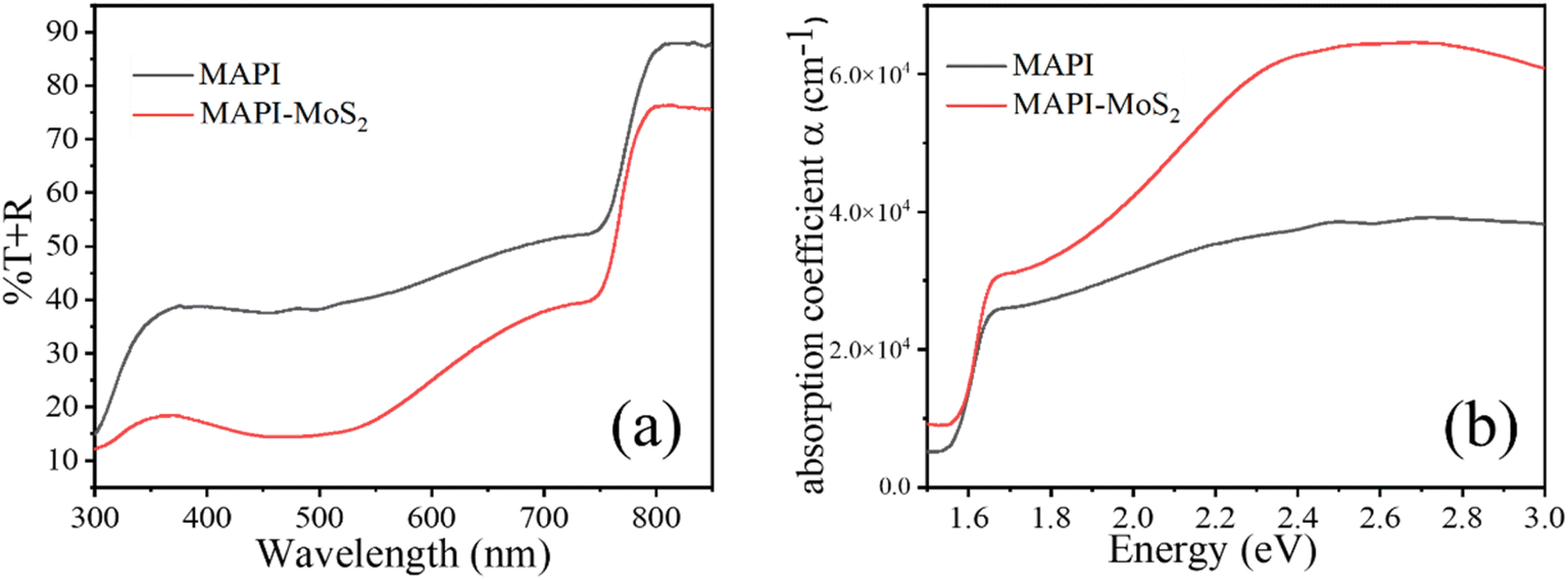 | ||
| Fig. 3 (a) UV-vis transmittance spectra of MAPI and MAPI–MoS2 films (0.4 mg mL−1); (b) absorption coefficient of MAPI and MAPI–MoS2 (0.4 mg mL−1) at different energies between 1.5 eV and 3 eV calculated from transmittance spectra. | ||
We also measured the Fermi level (EF) and valence band maximum (VBM) of MAPI and MoS2 QDs (Fig. 4) by ultraviolet photoelectron spectroscopy (UPS) and then determined the conduction band minimum (CBM) by adding the bandgap (Eg) obtained from Tauc plots of UV-vis measurements (Section-D in the ESI†).
 | ||
| Fig. 4 Experimental determination of the Fermi level of MAPI and MoS2 QDs from UPS measurements. The band gap was obtained from Tauc plots. The conduction band minimum (CBM) was determined by adding the band gap to the measured VBM. The corresponding energy diagram is also included. | ||
Based on these measurements, we have depicted the band energy diagram of MAPI and MoS2 QDs (Fig. 4). Unfortunately, neither the non-equilibrated nor the equilibrated energy level alignment between the QDs and MAPI is ideal for carrier generation in the QDs and subsequent transfer to MAPI for transport, specifically for the holes, as energy barriers will be formed at the valence band edges. However, we expect that in the presence of a sufficiently strong electric field, when the absorber layer becomes fully depleted, carriers may still tunnel through thinned energy barriers. This generally occurs even when energy level misalignment exists between perovskite absorbers and oxide transport layers.31–33 These observations justify further assessments and the investigation of the impact of the QDs on the performance of full device structures.
We therefore developed device test structures to evaluate the potential application of these composite films as the absorber layer for PV devices. In our device architectures we have used TiO2 as the electron transport layer (ETL) and Spiro-OMETAD as the hole transport layer (HTL). The detailed procedure for device fabrication is provided in the experimental section. The structure of the control device was ITO/TiO2/MAPI/Spiro-OMETAD/Au. Fig. 5a depicts the complete device stack with either MAPI or MAPI–MoS2 sandwiched between the ETL and HTL. In order to confirm the impact of incorporating MoS2 QDs in the MAPI absorber, devices were fabricated in two different laboratories by two different researchers' teams, resulting in two different device batches, B1 and B2. The same fabrication procedures were followed, except that B2 devices were fabricated in a glove box while B1 devices were produced in open air with active device areas of 4 mm2 (B1) and 25 mm2 (B2). A summary of average values of the performance parameters is provided in the table of Fig. 5b, where for instance the average PCE of B1-devices increased from 9.1% to 10.4% when QDs were introduced and B2-devices also showed improvements from 6.4% to 8.3%. Average values of the open circuit voltage (VOC), short-circuit current (JSC) and fill factor (FF) for all the different types of devices are also included in the table of Fig. 5b. In addition, the J–V characteristics of the champion device and complete statistical data of all the performance parameters for both B1 and B2 devices are included in the ESI (Fig. S10–S12†). Better device performance was achieved with B1-devices (Fig. 5b), while B2 devices were likely impacted by the larger device area, which highlights that improvements in the fabrication processes are required for large area deployment.26Fig. 5c and d reports the relative improvements with respect to MAPI-only devices for all four performance parameters in both device batches. The introduction of MoS2 QDs consistently increased the overall device PCE in both B1 and B2 devices (Fig. 5c and d) with average PCE improvements of 14% (B1) and by 28% (B2).
 | ||
| Fig. 5 (a) Diagram of the device structure. (b) Average device performance parameters. (c and d) Changes in performance parameter of the MAPI–MoS2 devices with respect to the corresponding MAPI-only devices for the two sets of solar cells prepared in different laboratories (B1 and B2): power conversion efficiency (PCE), open circuit voltage (VOC), short circuit current density (JSC) and fill factor (FF). | ||
The consistent increase in PCE directly result from relative improvements in the short circuit current density (JSC) for both B1 and B2 devices with MoS2 QDs (Fig. 5c and d). The increase in photocurrent can be attributed to enhanced carrier generation/collection as a result of the improved absorption coefficient (Fig. 3b) and possible MAPI defect passivation by MoS2 QDs. The open-circuit voltage (VOC) and fill factor (FF) exhibited smaller and mixed results, with a negative change of up to 9% in VOC for B2-devices and only a 4% change in FF for B1-devices, with negligible impact on the JSC and PCE improvements.
In order to understand better the impact of MoS2 QDs, we carried out further measurements on the B1 devices. Representative dark-current plots of MAPI-only and MAPI–MoS2 devices are shown in Fig. 6a, showing lower dark current in the composite film.
 | ||
| Fig. 6 (a) Typical dark current and (b) surface photovoltage spectroscopy of MAPI and MAPI–MoS2 devices from batch B1. | ||
The increase in dark current is caused by the migration of charge carriers due to the presence of defects, thus further supporting the presence of lower defect density in the composite film. The decrease in leakage current density also supports the passivation effect of MoS2. We also measured the surface photovoltage spectra of representative MAPI and MAPI–MoS2 films in the wavelength range of 500 nm to 1000 nm (Fig. 6b, B1-devices). The lower MAPI–MoS2 signal is indicative of better charge separation capacity compared to the MAPI-only film.34,35
To further assess the passivation effect of MoS2 QDs on the active layer and corresponding charge carrier recombination, electrochemical impedance spectroscopy (EIS) was performed (Fig. S9 in the ESI†). The obtained EIS spectra were best fitted using a previously reported model, considering a steady state concentration of the mobile carrier.36 Compared to the MAPI-only device, higher recombination resistance was observed for the MAPI–MoS2 device, indicating reduced charge carrier recombination losses due to the presence of MoS2 QDs in the active layer.19,37 The measurements of dark current together with surface photovoltage spectroscopy and electrochemical impedance spectroscopy provide independent and consistent evidence that the introduction of MoS2 QDs effectively passivates defects and enhances transport. These results are consistent with the higher PCE and short-circuit current density of the MAPI-MoS2 devices.
Overall MoS2 QDs contribute to enhanced light absorption as evidenced by the measured absorption coefficient shown in Fig. 3. This is directly reflected in an increased short-circuit current density and higher PCE. While the capture cross section of the MAPI interface defects is not expected to change, a reduced defect density, as suggested by dark current measurements (Fig. 6a), surface photovoltage spectroscopy (Fig. 6b) and electrochemical impedance spectroscopy (Fig. S9†), may have positively impacted the collection efficiency, thus contributing to higher device performance with QDs.
Carriers generated in the bulk MAPI layer are expected to dissociate at the interface with the corresponding transport layers. However, in this device architecture, the dissociation and transport of carriers generated within the QDs present a far more complex scenario. Carrier dissociation may occur at the MAPI–QD interface, for instance, facilitated by the electric field and by the electron affinity of the MoS2 QDs, which is more negative with respect to MAPI (Fig. 4). However, we should note that carriers may not dissociate at this interface and that excitons instead, i.e. carriers in their bound state, may transfer from the QDs to the MAPI, with dissociation occurring within the MAPI under the electric field or at the MAPI–transport layer interface.
Our results have therefore shown that while the device performance is improved, the energy level alignment is not ideal as it creates barriers that limit the collection efficiency of holes generated within the QDs or the transfer of excitons. Improvements in energy level alignment, which avoid the formation of barriers, could help harnessing the benefits of perovskite–QD composite layers, where for instance a type-I alignment should be favoured.21 This could be achieved for instance through appropriate material selection as well as by different forms of QD doping or surface engineering.38,39
With respect to device and film fabrication, it should be noted that the ionic liquid assisted grinding synthesis of MoS2 QDs is scalable and well-suited for the realization of large-area devices. In addition, the introduction of MoS2 QDs in the fabrication process does not require substantial additional steps and does not impact the scalability of the current perovskite solar cell fabrication methodologies. The chemical composition of MoS2 QDs also ensures that the environmental impact is limited and does not exacerbate existing challenges in deploying perovskite photovoltaics.
Conclusion
We have successfully incorporated MoS2 QDs into MAPI and highlighted the possibility of charge separation and collection with this configuration of carriers generated from the QDs. The alignment between the MAPI layer and MoS2 QDs can be further optimized to avoid the formation of energy barriers for carrier transport; however both passivation of MAPI defects and increased absorption have contributed to an overall increase in device efficiency. These results have been demonstrated in separate laboratories, confirming the consistency of the contribution from the QDs. The use of composite films integrating QDs is very promising not only for the specific MAPI–MoS2 pair but also for other materials that enable suitable band energy alignment, potentially paving the way toward high efficiency QDs solar cells.Data availability
This paper is accompanied by representative samples of experimental data and the relevant numerical tabulated raw data are available from the University of Strathclyde's Research Portal at https://doi.org/10.15129/a4aad5a4-1052-42bb-a31c-60fd167fd9b2. Detailed procedures explaining how these representative samples were selected, and how these experiments can be repeated, are provided in the corresponding sections of this paper. Additional results and raw data underlying this work are available in the ESI† or on request, following instructions provided at https://doi.org/10.15129/a4aad5a4-1052-42bb-a31c-60fd167fd9b2.Conflicts of interest
There are no conflicts to declare.Acknowledgements
This work was supported by the Department for Economy-Northern Ireland (award n.US146), Prof Mariotti's JSPS Invitation Fellowship and EPSRC (EP/R008841/1, EP/K022237/1 and EP/M024938/1). Dr Talitha R C Santos thanks CNPq and CAPES-PRINT for the fellowship.References
- J. Y. Kim, J. W. Lee, H. S. Jung, H. Shin and N. G. Park, High-Efficiency Perovskite Solar Cells, Chem. Rev., 2020, 120, 7867–7918 CrossRef CAS PubMed.
- A. K. Jena, A. Kulkarni and T. Miyasaka, Halide Perovskite Photovoltaics: Background, Status, and Future Prospects, Chem. Rev., 2019, 119, 3036–3103 CrossRef CAS PubMed.
- B. Ai, Z. Fan and Z. J. Wong, Plasmonic–perovskite solar cells, light emitters, and sensors, Microsyst. Nanoeng., 2022, 8, 5 CrossRef CAS PubMed.
- G. Abiram, M. Thanihaichelvan, P. Ravirajan and D. Velauthapillai, Review on Perovskite Semiconductor Field–Effect Transistors and Their Applications, Nanomaterials, 2022, 12, 2396 CrossRef CAS PubMed.
- O. Almora, D. Baran, G. C. Bazan, C. Berger, C. I. Cabrera, K. R. Catchpole, S. Erten-Ela, F. Guo, J. Hauch, A. W. Y. Ho-Baillie, T. J. Jacobsson, R. A. J. Janssen, T. Kirchartz, N. Kopidakis, Y. Li, M. A. Loi, R. R. Lunt, X. Mathew, M. D. McGehee, J. Min, D. B. Mitzi, M. K. Nazeeruddin, J. Nelson, A. F. Nogueira, U. W. Paetzold, N. Park, B. P. Rand, U. Rau, H. J. Snaith, E. Unger, L. Vaillant-Roca, H. Yip and C. J. Brabec, Device Performance of Emerging Photovoltaic Materials (Version 1), Adv. Energy Mater., 2021, 11, 2002774 CrossRef CAS.
- P. Wu, D. Thrithamarassery Gangadharan, M. I. Saidaminov and H. Tan, A Roadmap for Efficient and Stable All-Perovskite Tandem Solar Cells from a Chemistry Perspective, ACS Cent. Sci., 2023, 9, 14–26 CrossRef CAS PubMed.
- T. Moot, J. Werner, G. E. Eperon, K. Zhu, J. J. Berry, M. D. McGehee and J. M. Luther, Choose Your Own Adventure: Fabrication of Monolithic All-Perovskite Tandem Photovoltaics, Adv. Mater., 2020, 32, 2003312 CrossRef CAS PubMed.
- D. Sun, K. Zhang, S. Mei, J. Xu, Y. Jiang, X. Xiao, Y. Zhou and F. Mei, High performance perovskite LEDs via SPR and enhanced hole injection by incorporated MoS2, J. Phys. D Appl. Phys., 2021, 54, 214002 CrossRef CAS.
- M. Li, Q. Yin, R. Xu, X. Wang, X. Huang, Z. Chen, T. Ma, J. Chen and H. Zeng, Review on Anion Exchange of Lead-Halide Perovskite Nanocrystals: Process, Methods, and Applications, Adv. Eng. Mater., 2025, 27, 2401776 CrossRef CAS.
- I. C. Ciobotaru, C. C. Ciobotaru, C. Bartha, M. Enculescu, M. Secu, S. Polosan and C. Besleaga, Phase Transitions in Dimer/Layered Sb-Based Hybrid Halide Perovskites: An In-Depth Analysis of Structural and Spectroscopic Properties, Adv. Opt. Mater., 2025, 2402242 CrossRef CAS.
- M. F. Abdelbar, Q. Zhang, M. Abdelhameed, A. A. M. El-Amir, W. Jevasuwan, M. El-Kemary and N. Fukata, Spectral Downshifting and Passivation Effects Using 2D Perovskite (OAm)2SnBr4 Films to Enhance the Properties of Si Nanowire Solar Cells, ACS Appl. Energy Mater., 2023, 6, 4219–4228 CrossRef CAS.
- J. Yao, H. Liu, Z. Chen, B. Ma and L. Xu, Low-Dimensional Lead-Free Metal Halides for Efficient Electrically Driven Light-Emitting Diodes, Angew. Chem., Int. Ed., 2025, 64, e202423185 CrossRef CAS PubMed.
- H. Min, D. Y. Lee, J. Kim, G. Kim, K. S. Lee, J. Kim, M. J. Paik, Y. K. Kim, K. S. Kim, M. G. Kim, T. J. Shin and S. Il Seok, Perovskite solar cells with atomically coherent interlayers on SnO2 electrodes, Nature, 2021, 598, 444–450 CrossRef CAS PubMed.
- X. Luo, H. Luo, H. Li, R. Xia, X. Zheng, Z. Huang, Z. Liu, H. Gao, X. Zhang, S. Li, Z. Feng, Y. Chen and H. Tan, Efficient Perovskite/Silicon Tandem Solar Cells on Industrially Compatible Textured Silicon, Adv. Mater., 2023, 35, 2207883 CrossRef CAS PubMed.
- S. Mariotti, E. Kohnen, F. Scheler, K. Sveinbjornsson, L. Zimmermann, M. Piot, F. Yang, B. Li, J. Warby, A. Musiienko, D. Menzel, F. Lang, S. Kebler, I. Levine, D. Mantione, A. Al-Ashouri, M. S. Hartel, K. Xu, A. Cruz, J. Kurpiers, P. Wagner, H. Kobler, J. Li, A. Magomedov, D. Mecerreyes, E. Unger, A. Abate, M. Stolterfoht, B. Stannowski, R. Schlatmann, L. Korte and S. Albrecht, Interface engineering for high-performance, triple-halide perovskite–silicon tandem solar cells, Science, 2023,(381), 63–69 CrossRef CAS PubMed.
- M. I. Saleem, A. Batool and J. Hur, Cutting-Edge Developments in Metal Halide Perovskites Core/Shell Heterocrystals: from Photodetectors to Biomedical Applications, Small, 2025, 21, 2407032 CrossRef CAS PubMed.
- O. I. Kucheriv, D. A. Haleliuk, S. Shova and I. A. Gural’skiy, Fine-tuning of optical band gap in mixed halide aziridinium lead perovskites, Dalton Trans., 2025, 54, 1618–1624 RSC.
- D. Jariwala, A. R. Davoyan, J. Wong and H. A. Atwater, Van der Waals Materials for Atomically-Thin Photovoltaics: Promise and Outlook, ACS Photonics, 2017, 4, 2962–2970 CrossRef CAS.
- Z. Qin, Y. Chen, X. Wang, X. Liu, Y. Miao and Y. Zhao, Incorporation of Two-Dimensional WSe2into MAPbI3Perovskite for Efficient and Stable Photovoltaics, J. Phys. Chem. Lett., 2021, 12, 6883–6888 CrossRef CAS PubMed.
- A. U. Kambley, B. Alessi, C. McDonald, P. Papakonstantinou, V. Svrcek and D. Mariotti, Formamidinium lead iodide perovskite photovoltaics with MoS2 quantum dots, Sci. Rep., 2024, 14, 21613 CrossRef CAS PubMed.
- C. Rocks, V. Svrcek, T. Velusamy, M. Macias-Montero, P. Maguire and D. Mariotti, Type-I alignment in MAPbI3 based solar devices with doped-silicon nanocrystals, Nano Energy, 2018, 50, 245–255 CrossRef CAS.
- J. Cao, J. Yin, S. Yuan, Y. Zhao, J. Li and N. Zheng, Thiols as interfacial modifiers to enhance the performance and stability of perovskite solar cells, Nanoscale, 2015, 7, 9443–9447 RSC.
- J. Benson, M. Li, S. Wang, P. Wang and P. Papakonstantinou, Electrocatalytic Hydrogen Evolution Reaction on Edges of a Few Layer Molybdenum Disulfide Nanodots, ACS Appl. Mater. Interfaces, 2015, 7, 14113–14122 CrossRef CAS PubMed.
- N. Ahn, D. Y. Son, I. H. Jang, S. M. Kang, M. Choi and N. G. Park, Highly Reproducible Perovskite Solar Cells with Average Efficiency of 18.3% and Best Efficiency of 19.7% Fabricated via Lewis Base Adduct of Lead(II) Iodide, J. Am. Chem. Soc., 2015, 137, 8696–8699 CrossRef CAS PubMed.
- M. Saliba, J. P. Correa-Baena, C. M. Wolff, M. Stolterfoht, N. Phung, S. Albrecht, D. Neher and A. Abate, How to Make over 20% Efficient Perovskite Solar Cells in Regular (n-i-p) and Inverted (p-i-n) Architectures, Chem. Mater., 2018, 30, 4193–4201 CrossRef CAS.
- S. Chakrabarti, D. Carolan, B. Alessi, P. Maguire, V. Svrcek and D. Mariotti, Microplasma-synthesized ultra-small NiO nanocrystals, a ubiquitous hole transport material, Nanoscale Adv., 2019, 1, 4915–4925 RSC.
- A. Abate, M. Saliba, D. J. Hollman, S. D. Stranks, K. Wojciechowski, R. Avolio, G. Grancini, A. Petrozza and H. J. Snaith, Supramolecular halogen bond passivation of organic–inorganic halide perovskite solar cells, Nano Lett., 2014, 14, 3247–3254 CrossRef CAS PubMed.
- W. Huang, S. Sadhu and S. Ptasinska, Heat- and Gas-Induced Transformation in CH3NH3PbI3 Perovskites and Its Effect on the Efficiency of Solar Cells, Chem. Mater., 2017, 29, 8478–8485 CrossRef CAS.
- P. Pistor, A. Ruiz, A. Cabot and V. Izquierdo-Roca, Advanced Raman Spectroscopy of Methylammonium Lead Iodide: Development of a Non-destructive Characterisation Methodology, Sci. Rep., 2016, 6, 35973 CrossRef CAS PubMed.
- G. Xing, N. Mathews, S. Sun, S. S. Lim, Y. M. Lam, M. Gratzel, S. Mhaisalkar and T. C. Sum, Long-range balanced electron-and hole-transport lengths in organic–inorganic CH3NH3PbI3, Science, 2013, 342, 344–347 CrossRef CAS PubMed.
- S. S. Shin, S. J. Lee and S. Il Seok, Metal Oxide Charge Transport Layers for Efficient and Stable Perovskite Solar Cells, Adv. Funct. Mater., 2019, 29, 1900455 CrossRef CAS.
- J. Liu, S. Li, A. Mei and H. Han, Applications of Metal Oxide Charge Transport Layers in Perovskite Solar Cells, Small Sci., 2023, 3, 2300020 CrossRef CAS PubMed.
- L. Cai and F. Zhu, Toward efficient and stable operation of perovskite solar cells: Impact of sputtered metal oxide interlayers, Nano Sel., 2021, 2, 1417–1436 CrossRef CAS.
- B. N. Lee, S. Kirmayer, E. Edri, G. Hodes and D. Cahen, Surface photovoltage spectroscopy study of organo-lead perovskite solar cells, J. Phys. Chem. Lett., 2014, 5, 2408–2413 CrossRef PubMed.
- J. R. Harwell, T. K. Baikie, I. D. Baikie, J. L. Payne, C. Ni, J. T. S. Irvine, G. A. Turnbull and I. D. W. Samuel, Probing the energy levels of perovskite solar cells: via Kelvin probe and UV ambient pressure photoemission spectroscopy, Phys. Chem. Chem. Phys., 2016, 18, 19738–19745 RSC.
- A. R. C. Bredar, A. L. Chown, A. R. Burton and B. H. Farnum, Electrochemical Impedance Spectroscopy of Metal Oxide Electrodes for Energy Applications, ACS Appl. Energy Mater., 2020, 3, 66–98 CrossRef CAS.
- J. Shen, X. Ge, Q. Ge, N. Li, Y. Wang, X. Liu, J. Tao, T. He and S. Yang, Improvement of Photovoltaic Performance of Perovskite Solar Cells by Synergistic Modulation of SnO2 and Perovskite via Interfacial Modification, ACS Appl. Mater. Interfaces, 2024, 16, 24748–24759 CrossRef CAS PubMed.
- T. Velusamy, S. Mitra, M. Macias-Montero, V. Svrcek and D. Mariotti, Varying Surface Chemistries for p-Doped and n-Doped Silicon Nanocrystals and Impact on Photovoltaic Devices, ACS Appl. Mater. Interfaces, 2015, 7, 28207–28214 CrossRef CAS PubMed.
- A. ul Haq, M. Buerkle, B. Alessi, V. Svrcek, P. Maguire and D. Mariotti, Cluster-doping in silicon nanocrystals, Nanoscale Horiz., 2024, 9, 2042–2050 RSC.
Footnote |
| † Electronic supplementary information (ESI) available. See DOI: https://doi.org/10.1039/d5na00485c |
| This journal is © The Royal Society of Chemistry 2025 |