
 Open Access Article
 This Open Access Article is licensed under a Creative Commons Attribution-Non Commercial 3.0 Unported Licence
Flexible nanoimprinted substrate integrating piezoelectric potential and photonic-plasmonic resonances†
Aeshah F.
Alotaibi
 *ab,
Rongcheng
Gan
a,
Eni
Kume
a,
Dominik
Duleba
c,
Ahmed
Alanazi
a,
Allan
Finlay
a,
Robert P.
Johnson
c and
James H.
Rice
*a
*ab,
Rongcheng
Gan
a,
Eni
Kume
a,
Dominik
Duleba
c,
Ahmed
Alanazi
a,
Allan
Finlay
a,
Robert P.
Johnson
c and
James H.
Rice
*a
aSchool of Physics, University College Dublin, Belfield, Dublin 4, Ireland. E-mail: aeshah.alotaibi@ucdconnect.ie; rongcheng.gan@ucdconnect.ie; eni.kume@ucd.ie; ahmed.alanazi@ucdconnect.ie; allan.finlay@ucdconnect.ie; james.rice@ucd.ie
bDepartment of Physics, College of Science and Humanities, Shaqra University, Shaqra, Kingdom of Saudi Arabia
cSchool of Chemistry, University College Dublin, Belfield, Dublin 4, Ireland. E-mail: dominik.duleba@ucdconnect.ie; robert.johnson@ucd.ie
First published on 5th March 2025
Abstract
Flexible substrates for sensing provide adaptable, lightweight, and highly sensitive platforms for detecting different substances. The flexibility of these substrates allows for seamless integration with complex shapes and dynamic surfaces, enabling monitoring in challenging conditions using methods such as surface-enhanced Raman spectroscopy (SERS). Here we outline a flexible metamaterial array sensor formed from plasmonic silver-coated nanoimprinted piezoelectric polyvinylidene fluoride film. We show that nanoscale array features can be prepared on the surface of the piezoelectric film using a facile nanoimprinting procedure. These nanoimprinted features act as polarization channels that enable plasmonic resonances, enhancing the SERS signal strength and improving reproducibility. We combine this effect with the inherent piezoelectric properties of polyvinylidene fluoride to further enhance the Raman signal strength upon mechanical deformation. Our results demonstrate a significant enhancement of the SERS signal when probed at a wavelength of 532 nm, achieving over an order of magnitude increase in signal strength for a range of analytes. This lightweight and flexible SERS substrate holds significant potential for applications in medical diagnostics, environmental monitoring, and trace detection, offering a highly sensitive and reproducible analytical platform.
Introduction
Smart materials have properties that can change in response to external stimuli such as temperature, pressure, electric field, frequency, and other environmental factors.1,2 This ability to respond to various stimuli allows for fine-tuning of their functional properties, making them versatile for a wide range of applications. An example of such materials is the organic polymer polyvinylidene fluoride (PVDF), which can generate an electric charge under mechanical stress, exhibiting piezoelectric properties.3,4 These responsive characteristics have potential applications in the design of lightweight and flexible electronics, sensors, and energy harvesting devices.2–5 Recent advancements in the field have highlighted the growing role of piezoelectric materials in enhancing sensor performance and sensitivity.5 These studies have provided insights into the design and optimization of piezoelectric-based sensors for a wide range of applications.2,3The incorporation of nanomaterials, including nanoparticles, nanofibers, or nanotubes within the PVDF matrix, has gained significant attention in controlling the properties of the resulting composite material.4 An example of such an approach includes research into incorporating silver (Ag) nanostructures onto PVDF to augment electrical conductivity and stability, further enhancing piezoelectric performance.6 PVDF-Ag nanoparticle composites have been applied as analytical platforms to enhance the optical signal strength of plasmon-enhanced Raman scattering (SERS).7,8 The piezoelectric properties of the PVDF polymer enable the generation of electric charges upon mechanical stress, leading to amplified SERS signals and improved detection sensitivity. This enhancement in the SERS signal of approximately 10-fold has been reported to arise from piezoelectric changes migrating onto the Ag nanoparticles which enhances the SERS signals through the chemical enhancement factor.9,10 Ag nanoparticles on piezoelectric peptides showed that under mechanical stress have been reported to support SERS signal intensity increases of more than an order of magnitude11,12 Finite-element electromagnetics simulations of the system showed that the piezoelectric-based electric field induces internal fields that work cooperatively to boost the SERS signal.10,12 Thus, the signal enhancement is attributed to charge transfer between the piezoelectric peptide and the Ag nanoparticles. This additional charge on the Ag nanoparticle alters the localized surface plasmon resonance which can yield an enhancement in SERS signal strength. Such studies demonstrate that through a judicious combination of piezoelectric and plasmonic materials the amplification of Raman scattering signals can be achieved, beyond that achievable using the materials separately. This enables lower concentrations of analytes to be detected which is of significance in areas such as biosensing,13 or trace detection.14
Nanoimprinting can form precise and reproducible surface features into polymers15–18 which can be coated with a thin (ex. 15 nm) layer of plasmon active metal. By optimizing the size and period of the nanoscale features photonic resonances can be engineered into the structure ensuring coupling of the light with plasmon modes, with multiple plasmon modes often being generated, resulting in interaction and mixing processes. These modes can enhance optical detection such as those based on Raman scattering or fluorescence. Studies have shown that Ag-coated nanoimprinted cellulose acetate enhances SERS signal strengths by >10-fold relative to flat surfaces.15 This enhancement potentially arises from Bragg modes which propagative surface plasmons localized by the diffraction from the plasmonic-coated nanostructure arrays.19 This generates surface-guided modes, localized as standing waves, leading to highly confined fields. In this work, we demonstrate a facile method for imprinting nanosized features into the surface of PVDF creating a plasmon active metamaterial surface array. The properties of which are combined with the piezoelectric properties of the PVDF film to create an efficient sensor platform. We demonstrate that this substrate boosts surface-enhanced Raman spectroscopy (SERS) signals by combining both photonic, electromagnetic, and piezoelectric-based mechanisms. This lightweight and flexible substrate design has potential applications in several areas such as medical diagnostics and environmental monitoring.
Results and discussion
Substrate design and engineered properties
Nanoimprinted PVDF substrates were prepared using a soft imprinted-based approach (illustrated in Fig. 1(a) and outlined in ESI†). In brief, a PVDF solution was uniformly applied onto a linear silicon nanostamp. Following drying, the PVDF polymer film was then removed from the stamp. The resulting PVDF polymer has imprinted on its surface features that replicate the silicon master. The PVDF film is then coated with a plasmon active metal (e.g. Ag). The nanoimprinted PVDF film was covered by an Ag film of 10 nm which is a film thickness that is effective at enhancing SERS.20,21 The resulting PVDF film exhibits structural coloration (Fig. 1(b)) arising from interference and plasmonic resonance effects due to the imprinted nanostructures. | ||
| Fig. 1 (a) A schematic illustration of the fabrication process of the nanoimprinted PVDF piezoelectric film. (b) Photos of the resulting nanoimprinted PVDF before and after coating with Ag. The presence of optical diffraction can be seen arising from the imprinted PVDF. (c) SERS studies using the Ag-coated nanoimprinted PVDF film. (d(i)) SERS enhancement arising from the nanoimprinted features. (ii) SERS enhancement arising from piezoelectric potential accelerated through mechanical deformation. (iii) The boosting of the SERS signal through combining enhancement effects arising from nanoimprinted features and piezoelectric potential. | ||
The nanoimprinted PVDF film when applied as a SERS substrate (Fig. 1(c)). The nanoscale features on the PVDFs surface can possess photonic resonances which can mix with Ag plasmonic resonances yielding an enhancement in SERS signal relative to a flat film (Fig. 1(d(i))). Additionally, the piezoelectric potential of PVDF can be activated through mechanical deformation.9 The applied mechanical deformation is converted into stored electrical energy. This yields a negative electric potential on the substrate surface which injects electrical energy into Ag. The piezoelectric charges transfer to the plasmonic metal creating an enhancement in the electromagnetic field10,12 arising from the metal's plasmon resonance. SERS intensities are proportional to the fourth power of the electromagnetic field, resulting in the intensities of SERS spectra being significantly enhanced.22 This yields an enhancement of the SERS signal (Fig. 1(d(ii))). The design of the substrate combines both piezoelectric and photonic resonance-based enhancement mechanisms to boost SERS signals (Fig. 1(d(iii))) beyond them separately.
AFM tapping-mode imaging of the nanoimprinted PVDF surface features was undertaken (Fig. 2(a)) to provide high-resolution imaging while preserving the integrity of the nanoimprinted structures. The AFM image revealed a linear grating-like structure. AFM plot profiles (inset of Fig. 2(a)) show that the linear array has average dimensions of 414 ± 5.8 nm, a groove depth of 198 ± 7.2 nm, a line separation width of 226 ± 8.2 nm, and an average height of PVDF nanoimprinted lines around 155.525 ± 6.06 nm. Following the deposition of Ag, the feature sizes imprinted on the surface of the polymer are visible, with a noticeable change in these dimensions (Fig. 2(b)). The feature sizes of Ag-coated imprinted PVDF indicate a linear period of 433.8 ± 7.92 nm, a groove depth of 162 ± 7.15 nm, and a line width of 284 ± 4.83 nm. Plot profiles meticulously outlined the linear structures, highlighting their precise dimensions, with an average height of around 181.25 ± 6.06 nm.
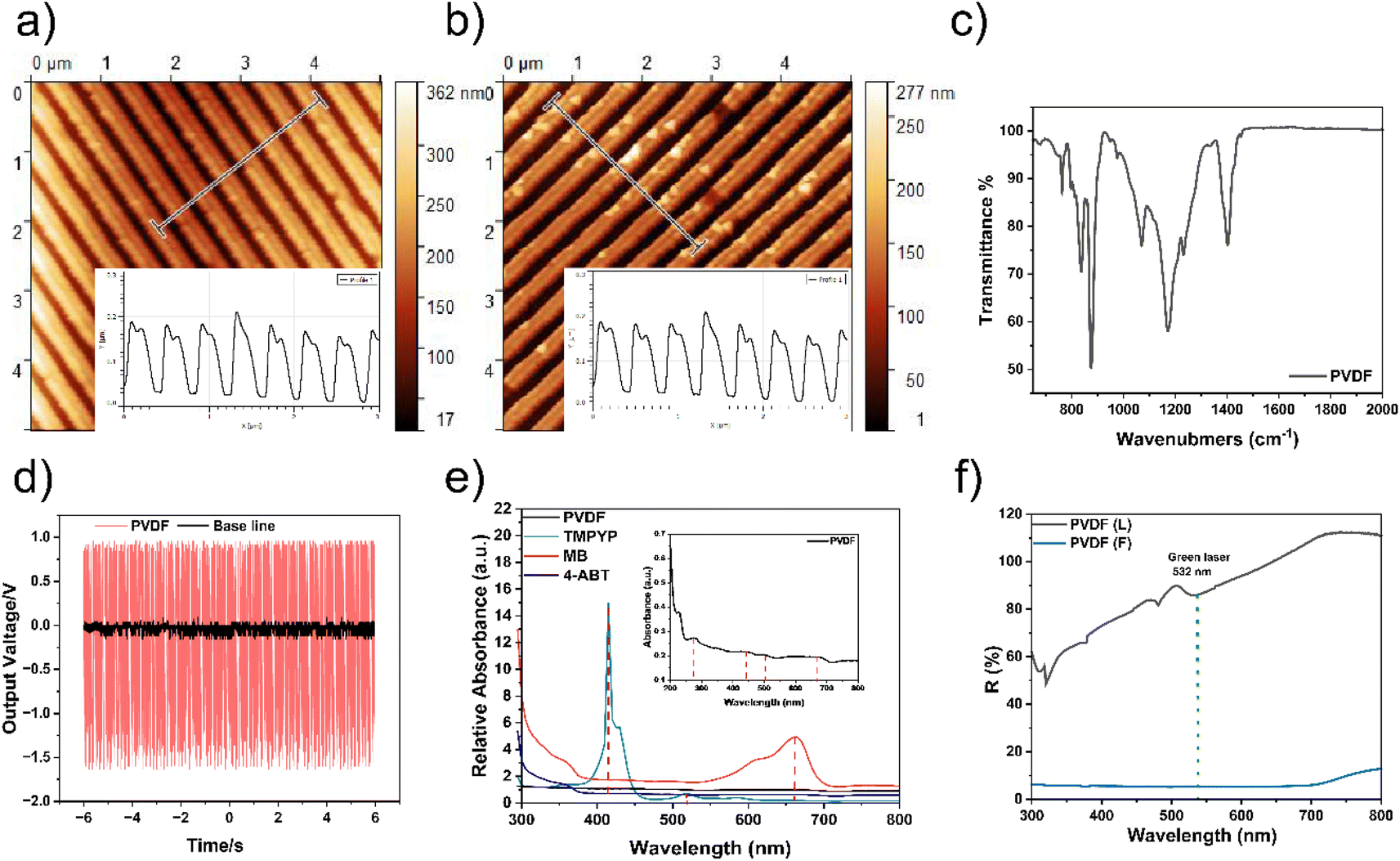 | ||
| Fig. 2 (a and b) Two AFM images of nanoimprinted PVDF. Inserts shows a plot of height vs. distance to profile the topography of the sample. (a) Shows the imprinted PVDF before adding a silver layer, (b) was recorded after a layer of silver was added to the surface of the imprinted PVDF. (c) Infrared absorption (FTIR) spectra FTIR of PVDF. Shown are band positions assigned to the α or β phases that the polymer. (d) The current voltage plot for PVDF. The voltage output is indicative of strong piezoelectric potential. (e) Reflection spectra for PVDF before imprinting e.g. flat (F) and following imprinting (L). (f) Optical absorption measurements of the probe molecules and PVDF film before silver coating. | ||
Polyvinylidene fluoride (PVDF) encompasses three primary crystalline phases—alpha (α), beta (β), and gamma (γ)—each distinguished by unique infrared absorption spectra signatures.23 Enhanced dipole moments and increased molecular order in the β-phase contribute to superior piezoelectric properties.3,6,23 The infrared absorption spectrum of the nanoimprinted PVDF substrate (Fig. 2(c)) exhibits distinct absorption bands, a hallmark of PVDF's crystalline phases. These phases, each possessing unique vibrational signatures, are inherent to PVDF.3,6,23 The spectral features align with the α and β phases, indicating the successful formation of PVDF's electroactive phases during the nanoimprinting process. This process demonstrates the ability to induce phase transformations in PVDF, enhancing its piezoelectric properties. The piezoelectric properties of the sample are confirmed by electrical measurements. The nanoimprinted PVDF piezoelectric film (Fig. 2(d)) shows a approximately 1 V output upon mechanical stress being applied to the sample. Resulting from piezoelectric potential being activated. The optical absorption of the PVDF film before silver coating (Fig. 2(e)) shows no absorption features in the visible region. This arises as the polymer is a wide band gap semiconductor (Eg ∼ 6 eV).1 Optical reflection measurements provided valuable insights into the interaction between the nanostructured PVDF films and incident light (Fig. 2(f)). The presence of linear nanostructures, coupled with the Ag coating, influenced the reflection spectra, leading to alterations in the films' optical properties. The UV-vis reflection data shows peaks and dips, indicative of the films' nanoimprinted features. Dips at 530 and 480 nm have been observed along with additional features at 420 and 360 nm. Such spectroscopic features are not present in a flat/unimprinted film indicating that the nanoarray features give rise to the distinct dips/peaks in the reflection spectra (Fig. 2(e)). These features potentially arise from resonant peaks corresponding to localized plasmonic modes of the nanoarray and/or coupled plasmonic modes.15,16,24 Such coupled modes arise from the interaction between neighbouring plasmonic nanofeatures in the imprinted array leading to coupled plasmonic modes.24
Photonic and piezoelectric-enhanced SERS detection
The properties of the Ag-coated imprinted PVDF substrate design were examined by first looking at the effect of the imprinted features on the Raman enhancement factor (EF). COMSOL Multiphysics modeling of the electric field generated by the localized surface plasmons on imprinted samples was undertaken. An electric field map (Fig. 3(a)) from a single 2D nanoimprinted array feature shows the largest fields are generated on the edges of the square-like nanostructure. The simulated Raman enhancement factor of these imprinted structures (Fig. 3(a)) shows strong enhancement at approximately 430 and 500 nm arising from transverse and longitudinal localized plasmon modes of the nanoimprinted structure respectively. The optical reflection spectrum for the Ag-coated imprinted PVDF substrate (Fig. 2(e)) shows a drop (dip) in reflectance at approximately 530 nm potentially arising from absorption by the longitudinal mode in the substrate. On this basis, a Raman excitation wavelength of 532 nm was selected to probe the SERS from Ag-coated imprinted PVDF thin film samples. | ||
| Fig. 3 COMSOL and SERS spectra were recorded on Ag-coated imprinted PVDF. (a) COMSOL simulation of a single imprinted feature showing electric field distribution, also shown is a plot of simulated Raman enhancement factor as a function of wavelength generated from the single imprinted feature. (b) SERS from 4ABT (10−5 M) on a flat (red) and imprinted (black) Ag-coated PVDF. (c) A plot of SERS signal intensity for 1436 cm−1 Raman peak over different spots on the substrate. (d) SERS spectra were recorded with various concentrations of 4ABT from 10−4 to 10−11 M. (e) Plot of 1436 cm−1 peak intensity vs. concentration. | ||
The SERS spectra of 4ABT were recorded on Ag-coated imprinted PVDF and flat Ag-coated PVDF (e.g. no imprinted features) (Fig. 3(b)). The SERS spectra show peaks at 1075 and 1594 cm−1 with additional peaks located at 1140, 1388, and 1438 cm−1 in line with literature reports.25–27 The SERS signal from the nanoimprinted sample is significantly stronger than from the unimprinted substrate. The Raman EF of the nanoimprinted SERS substrate (without the piezoelectric enhancement) was calculated to be 9 × 10⁵ using a spectrum of the 10−5 M sample as a reference, with silicon substrate serving as the benchmark for the normal Raman substrate. Our EF is similar to EFs reported for nanograting systems, for example, EF of 2 × 10⁶ and a limit of detection (LOD) of 10−9 M being reported for laser-written gold nano gratings fabricated on silicon.28 While EF of >1 × 10⁵ and a limit of detection (LOD) of 10−8 M were reported for grating formed by laser patterning of poly(methyl methacrylate) followed by silver evaporation.29 This demonstrates that the imprinted surface features significantly improve the SERS EF. The signal reproducibility was then studied by plotting the SERS signal for 4ABT from 20 randomly chosen spots on the substrate. Good SERS signal reproducibility over the sample (Fig. 3(c)) was observed with a relative standard deviation of the SERS peak at 1438 cm−1 calculated to be <11%. The sample possesses long-range uniformity resulting in the electromagnetic “hot spots” supporting reproducible SERS signal strengths, with variation in the Raman signal potentially arising from concentration variation in the probe molecule surface across the sample. SERS intensity exhibited a concentration-dependent increase (Fig. 3(d and e)), showing a linear correlation with 4ABT concentration, as depicted in Fig. 3(d) with the signals down to 10−11 M sample being detected.
COMSOL simulations (Fig. 4(a)) were undertaken to examine the impact of applying a weight to the surface of the Ag-coated imprinted PVDF substrate. Where the applied weight acts as a force causing mechanical deformation of the semiconductor plastic creating a piezoelectric potential. A COMSOL-generated electric field map (Fig. 4(a)) of a single 2D nanoimprinted array feature before and after the mechanical force was applied was simulated. As outlined above before force is applied the imprinted nanostructure shows electric field resonances strongest on the edges of the square-like imprinted structure. Following an applied force to the substrate, the electric field intensity increases. Particularly at the edges of the nanostructure (Fig. 4(a)). Simulations of Raman EF as a function of spectral wavelength were then undertaken and plotted, before and after weight was applied to the substrate (Fig. 4(a)). This simulation showed an increase in electric field intensity supports an increase in Raman EF of 9-fold following the application of a 500 g weight. Inspection of the simulated spectrum of the Raman enhancement factor (Fig. 4(a)) shows that the maximum enhancement occurs at approximately 520 nm, which is a redshift of 20 nm compared to the maxima Raman enhancement factor wavelength for the sample before a force is applied. This increase and red-shift in the Raman enhancement factor potentially occur through charge transfer between the piezoelectric polymer and the plasmonic nanofeature. This increase in charge density on the plasmonic material affects the electromagnetic field strength boosting the SERS signal. Studies30,31 have shown that increasing the charge density on plasmonic (silver) nanofeatures creates a red shift in the maxima of the plasmon resonance, as well as an increase in electric field strength resulting in increased SERS signals.
 | ||
| Fig. 4 (a(i)) COMSOL simulations of electric field distribution (ii) simulated Raman enhancement factor as a function of wavelength for a single imprinted feature showing electric field distribution before and after 500-gram weight was added and (iii) SERS spectra at different pressure. (b) SERS spectra for 4ABT on the substrate, with a weight or load added (black) and then removed (green). (c) A plot of SERS signal intensity for the substrate with an added weight and then with the weight removed repeated 10 times. (d) The SERS intensity at the 1436.25 cm−1 peak of 4-ABT increases with incremental weights (0, 100, 200, and 400 g). (e) SERS spectra for TMPyP on the substrate, with a weight or load added (black) and then removed (green). (f) SERS spectra for a third probe molecule MB with a weight or load added by finger pressing the surface of the substrate (black) and then after removing the applied force (green) for a probe molecule concentration of 10−5 M and 10−10 M. | ||
To assess the contribution of piezoelectricity to the Raman EF, a 4ABT 10−5 M sample was selected as a representative case. Applying a weight of 200 g at a 5 mm distance from the incident laser spot on the samples served as a strategic approach to enhance piezoelectric properties. The application of this force on the substrate during the Raman scattering process resulted in an average 1.4-fold amplification (Fig. 4(b and c)) of the signal of the representative peak. Leading to an increased EF, to 1.3 × 10⁶ from EF = 9 × 10⁵ obtained without piezoelectric enhancement. The Raman EF increase been proportional to the applied weight. In the (Fig. S1, ESI†) demonstrates how applying pressure to a PVDF/Ag-coated system with a probe molecule enhances SERS performance. When a 200 g force is applied, the piezoelectric properties of PVDF generate an electric field across the Ag, shifting its Fermi level and intensifying the local electromagnetic field around the probe molecule. This electric field enhances charge transfer and local field intensity, leading to a stronger Raman signal under applied pressure. COMSOL calculations (Fig. 4a(iii)) show that as the weight added to the substrate increases the Raman enhancement factor also increases. SERS measurements were undertaken applying different weights (Fig. 4(d)) showed that the SERS signal strength increased with an increase in the applied weight. To assess the role of PVDF's piezoelectric properties in SERS enhancement, a control experiment was conducted using a non-piezoelectric PDMS/Ag grating system with methylene blue (MB) as the probe molecule (Fig. S3, ESI†). Unlike the PVDF/Ag system, which shows increased SERS intensity under pressure due to PVDF's electric field generation and Fermi level modulation, the PDMS/Ag system displays decreased SERS intensity when compressed, highlighting the essential role of PVDF's piezoelectric effect in pressure-induced SERS enhancement.
To broaden the evaluation of sensing performance for typical probe molecules, we conducted additional studies testing the porphyrin TMPyP32,33 with and without piezoelectric enhancement (Fig. 4(e)). Following the application of a 200 g load a Raman EF = 1.3 was observed regarding an increase in SERS intensity. As outlined in the above COMSOL simulations the inherent piezoelectric characteristics of the PVDF film generate an electric field under mechanical stress, intensifying the interaction between the probe molecule and the substrate. Resulting in an amplified near-field effect yielding stronger SERS signals. Mechanical deformation of PVDF through the application of external pressure during SERS measurements modulates the piezoelectric potential, influencing near-field enhancement and culminating in increased SERS EF. The subsequent relaxation of the piezoelectric enhanced SERS signal (Fig. 4(e)) back to the original SERS signal level occurs following the removal of the applied force. Highlighting the reversibility of these mechanical-induced changes. The LOD of the piezoelectrically enhanced SERS substrates was also evaluated for a third probe molecule methylene blue (MB) prepared at 10−5 M, and 10−9 M. Following piezoelectric activation enhanced SERS signal intensity can be seen when additional pressure was applied (Fig. 4(f)). The MB SERS Raman band at 1622 cm−1 has been enhanced 1.5 times enabling MB to be more easily detected at low concentrations.
Conclusion
In conclusion, the flexible nanoimprinted piezoelectric-plasmonic substrate demonstrates significantly enhanced SERS performance. This enhancement arises from the synergistic interplay between piezoelectric-induced polarization channels, plasmonic resonances, and the nanoscale features imprinted on the substrate. These mechanisms collectively amplify the localized electromagnetic fields at the surface, enabling stronger interactions with target molecules and improving detection sensitivity. COMSOL simulations support this by revealing electromagnetic hot spots generated by the nanostructures, further amplified under mechanical stress through piezoelectric charge generation. This lightweight and flexible substrate holds great promise for diverse applications, including medical diagnostics, environmental monitoring, and trace detection. Future work will focus on optimizing these parameters to push the boundaries of sensitivity and extend its applicability across various fields.Data availability
The datasets supporting the findings of this study are openly available in the Research Repository UCD. These include the data generated and analyzed during the current study. All relevant code and additional material are also available in the ESI attached to the manuscript.†Author contributions
A. F. A., R. G., and J. H. R. conceptualized and designed the experiments, as well as developed the experimental apparatus. A. F. A. and R. G. conducted the sample preparation, AFM, electrical measurements, and Raman spectroscopy. Reflection spectroscopy was performed by A. F. A., and A. A. UV-vis measurements were carried out by A. F. A. and A. F. FTIR measurements were executed by A. F. A. and E. K. D. D. performed the simulations using COMSOL software. All authors contributed to data analysis, discussed the results, and participated in the writing and review of the manuscript.Conflicts of interest
The authors declare no competing interests.Acknowledgements
This research was generously supported by the Ministry of Education in the Kingdom of Saudi Arabia (MOE) through Shaqra University, in partnership with the Saudi Arabian Cultural Mission (SACM). We sincerely appreciate their financial assistance, which significantly contributed to the successful completion of this study. The authors express their sincere gratitude to Brian Rodriguez for providing access to the AFM instrumentation and to David Browne for facilitating access to the UV-vis reflection spectroscopy. Special thanks go to Joe Branson for his invaluable assistance with the silver coating and to Aoife Cowen for her support with the FTIR measurements.References
- S. D. Mahapatra, P. C. Mohapatra, A. I. Aria, G. Christie, Y. K. Mishra, S. Hofmann and V. K. Thakur, Piezoelectric materials for energy harvesting and sensing applications: Roadmap for future smart materials, Adv. Sci., 2021, 8(17), 2100864, DOI:10.1002/advs.202100864.
- Y. Wu, T. Sun, M. Shao, C. Ji, C. Li, C. Zhang and Z. Li, Pyroelectrically Driven Charge Transfer and its Advantages on SERS and Self-Cleaning Property, Laser Photonics Rev., 2024, 19(4), 2401152, DOI:10.1002/lpor.202401152.
- X. Wan, H. Cong, G. Jiang, X. Liang, L. Liu and H. He, A Review on PVDF Nanofibers in Textiles for Flexible Piezoelectric Sensors, ACS Appl. Nano Mater., 2023, 6(3), 1522–1540, DOI:10.1021/acsanm.2c04916.
- D. T. Alvarez-Ruiz, S. Almohammed, A. Fularz, S. T. Barwich and J. H. Rice, Self-energized organic-inorganic hybrid composite for surface enhanced Raman spectroscopy, J. Appl. Phys., 2021, 129(19), 1–8, DOI:10.1063/5.0048802.
- Y. Liu, S. Qiao, C. Fang, Y. He, H. Sun, J. Liu and Y. Ma, A highly sensitive LITES sensor based on a multi-pass cell with dense spot pattern and a novel quartz tuning fork with low frequency, Opto-Electron. Adv., 2024, 7(3), 230230, DOI:10.29026/oea.2024.230230.
- M. Yan, S. Liu, Y. Liu, Z. Xiao, X. Yuan, D. Zhai, K. Zhou, Q. Wang, D. Zhang, C. Bowen and Y. Zhang, Flexible PVDF–TrFE Nanocomposites with Ag-decorated BCZT Heterostructures for Piezoelectric Nanogenerator Applications, ACS Appl. Mater. Interfaces, 2022, 14(47), 53261–53273, DOI:10.1021/acsami.2c15581.
- H. Li, H. Dai, Y. Zhang, W. Tong, H. Gao and Q. An, Surface-Enhanced Raman Spectra Promoted by a Finger Press in an All-Solid-State Flexible Energy Conversion and Storage Film, Angew. Chem., Int. Ed., 2017, 56(10), 2649–2654, DOI:10.1002/anie.201610737.
- H. Li, H. Yin, H. Dai, H. K. Lee, Y. Cui, F. Sun, Y. Zhang and Q. An, Enriching surface-enhanced Raman spectral signatures in combined static and plasmonic electrical fields in self-powered substrates, Nano Energy, 2022, 92, 106737, DOI:10.1016/j.nanoen.2021.106737.
- J. Lu, Y. Song, F. Lei, X. Du, Y. Huo, S. Xu, C. Li, T. Ning, J. Yu and C. Zhang, Electric Field-Modulated Surface Enhanced Raman Spectroscopy by PVDF/Ag Hybrid, Sci. Rep., 2020, 10(1), 5269, DOI:10.1038/s41598-020-62251-0.
- S. Almohammed, A. Fularz, F. Zhang, D. Alvarez-Ruiz, F. Bello, D. D. O'Regan, B. J. Rodriguez and J. H. Rice, Flexing Piezoelectric Diphenylalanine–Plasmonic Metal Nanocomposites to Increase SERS Signal Strength, ACS Appl. Mater. Interfaces, 2020, 12(43), 48874–48881, DOI:10.1021/acsami.0c15498.
- S. Almohammed, A. Fularz, M. B. Kanoun, S. Goumri-Said, A. Aljaafari, B. J. Rodriguez and J. H. Rice, Structural Transition-Induced Raman Enhancement in Bioinspired Diphenylalanine Peptide Nanotubes, ACS Appl. Mater. Interfaces, 2022, 14(10), 12504–12514, DOI:10.1021/acsami.1c22770.
- S. Almohammed, A. Finlay, D. Duleba, S. Cosgrave, R. Johnson, B. J. Rodriguez and J. H. Rice, Piezoelectric Peptide Nanotube Substrate Sensors Activated through Sound Wave Energy, ACS Mater. Lett., 2024, 6(5), 1863–1869, DOI:10.1021/acsmaterialslett.3c01613.
- S. Almohammed, B. J. Rodriguez and J. H. Rice, Nucleobase sensing using highly-sensitive surface-enhanced Raman spectroscopy templates comprising organic semiconductor peptide nanotubes and metal nanoparticles, Sens. Bio-Sens. Res., 2019, 24, 100287, DOI:10.1016/j.sbsr.2019.100287.
- S. Almohammed, S. Fedele, B. J. Rodriguez and J. H. Rice, Aligned diphenylalanine nanotube–silver nanoparticle templates for high-sensitivity surface-enhanced Raman scattering, J. Raman Spectrosc., 2017, 48(12), 1799–1807, DOI:10.1002/jrs.5254.
- A. Fularz, D. Stogiannis and J. H. Rice, Cellulose Acetate-Based Plasmonic Crystals for Surface-Enhanced Raman and Fluorescence Spectroscopy, ACS Mater. Au, 2022, 2(4), 453–463, DOI:10.1021/acsmaterialsau.2c00013.
- A. Espinha, C. Dore, C. Matricardi, M. I. Alonso, A. R. Goñi and A. Mihi, Hydroxypropyl cellulose photonic architectures by soft nanoimprinting lithography, Nat. Photonics, 2018, 12(6), 343–348, DOI:10.1038/s41566-018-0152-1.
- A. F. Alotaibi, A. Alanazi, A. Lesniak-Podsiadlo, A. Cowen, B. J. Rodriguez and J. H. Rice, Nanoimprinted cellulose acetate-TiO2 composite thin film, Photon. Nanostruct: Fundam. Appl., 2024, 59, 101257, DOI:10.1016/j.photonics.2024.101257.
- A. F. Alotaibi, B. J. Rodriguez and J. H. Rice, A nano-imprinted graphene oxide-cellulose composite as a SERS active substrate, Anal. Methods, 2024, 16(21), 3385–3391, 10.1039/d4ay00749b.
- J. Jiang, X. Wang, S. Li, F. Ding, N. Li, S. Meng, R. Li, J. Qi, Q. Liu and G. L. Liu, Plasmonic nano-arrays for ultrasensitive bio-sensing, Nanophotonics, 2018, 7(9), 1517–1531, DOI:10.1515/nanoph-2018-0023.
- H. Schneidewind, K. Weber, M. Zeisberger, U. Hübner, A. Dellith, D. Cialla-May, R. Mattheis and J. Popp, The effect of silver thickness on the enhancement of polymer based SERS substrates, Nanotechnology, 2014, 25(44), 445203, DOI:10.1088/0957-4484/25/44/445203.
- C. Lee, C. S. Robertson, A. H. Nguyen, M. Kahraman and S. Wachsmann-Hogiu, Thickness of a metallic film, in addition to its roughness, plays a significant role in SERS activity, Sci. Rep., 2015, 5(1), 11644, DOI:10.1038/srep11644.
- K. Kneipp, M. Moskovits, and H. Kneipp, Surface-Enhanced Raman Scattering, Springer Science & Business Media, 2006, http://books.google.ie/books?id=5xlTw9WCUwEC%26printsec=frontcover%26dq=Schatz,+G.C.,+Young,+M.A.+and+Van+Duyne,+R.P.,+2006.+Electromagnetic+mechanism+of+SERS.+In%C2%A0Surface-enhanced+Raman+scattering:+physics+and+applications%C2%A0(pp.+19-45).+Berlin,+Heidelberg Search PubMed.
- X. Cai, T. Lei, D. Sun and L. Lin, A critical analysis of the α, β and γ phases in poly(vinylidene fluoride) using FTIR, RSC Adv., 2017, 7(25), 15382–15389, 10.1039/c7ra01267e.
- Y. Zheng, A. H. Soeriyadi, L. Rosa, S. H. Ng, U. Bach and J. J. Gooding, Reversible gating of smart plasmonic molecular traps using thermoresponsive polymers for single-molecule detection, Nat. Commun., 2015, 6(1), 8797, DOI:10.1038/ncomms9797.
- S. Almohammed, M. Alruwaili, E. G. Reynaud, G. Redmond, J. H. Rice and B. J. Rodriguez, 3D-Printed Peptide-Hydrogel Nanoparticle Composites for Surface-Enhanced Raman Spectroscopy Sensing, ACS Appl. Nano Mater., 2019, 2(8), 5029–5034, DOI:10.1021/acsanm.9b00940.
- R. M. Al-Shammari, M. A. Baghban, N. Al-Attar, A. Gowen, K. Gallo, J. H. Rice and B. J. Rodriguez, Photoinduced Enhanced Raman from Lithium Niobate on Insulator Template, ACS Appl. Mater. Interfaces, 2018, 10(36), 30871–30878, DOI:10.1021/acsami.8b10076.
- S. Damm, F. Lordan, A. Murphy, M. McMillen, R. Pollard and J. H. Rice, Application of AAO Matrix in Aligned Gold Nanorod Array Substrates for Surface-Enhanced Fluorescence and Raman Scattering, Plasmonics, 2014, 9(6), 1371–1376, DOI:10.1007/s11468-014-9751-y.
- Z. Ma, Y. Zhang, B. Han, X. Liu, H. Zhang, Q. Chen and H. Sun, Femtosecond Laser Direct Writing of Plasmonic Ag/Pd Alloy Nanostructures Enables Flexible Integration of Robust SERS Substrates, Adv. Mater. Technol., 2017, 2(6), 1600270, DOI:10.1002/admt.201600270.
- Y. C. Chang, B. H. Huang and T. H. Lin, Surface-Enhanced Raman Scattering and Fluorescence on Gold Nanogratings, Nanomaterials, 2020, 10(4), 776, DOI:10.3390/nano10040776.
- A. T. Alanazi and J. H. Rice, Hybrid composite based on conducting polymers and plasmonic nanomaterials applied to catalysis and sensing, Mater. Res. Express, 2022, 9(7), 075002, DOI:10.1088/2053-1591/ac7d9a.
- S. Almohammed, F. Zhang, B. J. Rodriguez and J. H. Rice, Photo-induced surface-enhanced Raman spectroscopy from a diphenylalanine peptide nanotube-metal nanoparticle template, Sci. Rep., 2018, 8(1), 3880, DOI:10.1038/s41598-018-22269-x.
- S. Ferdele, B. Jose, R. Foster, T. E. Keyes and J. H. Rice, Strong coupling in porphyrin J-aggregate excitons and plasmons in nano-void arrays, Opt. Mater., 2017, 72, 680–684, DOI:10.1016/j.optmat.2017.07.018.
- M. H. V. Reddy, R. M. Al-Shammari, N. Al-Attar, E. Kennedy, L. Rogers, S. Lopez, M. O. Senge, T. E. Keyes and J. H. Rice, Micro- or nanorod and nanosphere structures derived from a series of phenyl-porphyrins, Phys. Chem. Chem. Phys., 2014, 16(9), 4386–4393, 10.1039/c3cp54936d.
Footnote |
| † Electronic supplementary information (ESI) available. See DOI: https://doi.org/10.1039/d4na00942h |
| This journal is © The Royal Society of Chemistry 2025 |