
 Open Access Article
 This Open Access Article is licensed under a Creative Commons Attribution-Non Commercial 3.0 Unported Licence
Advances in core technologies for semiconductor manufacturing: applications and challenges of atomic layer etching, neutral beam etching and atomic layer deposition
Tzu-Yi
Lee†
 ab,
Pei-Tien
Chen†
a,
Chien-Chi
Huang†
a,
Hsin-Chu
Chen
*c,
Li-Yin
Chen
a,
Po-Tsung
Lee
a,
Fang-Chung
Chen
a,
Ray-Hua
Horng
d and
Hao-Chung
Kuo
*ab
ab,
Pei-Tien
Chen†
a,
Chien-Chi
Huang†
a,
Hsin-Chu
Chen
*c,
Li-Yin
Chen
a,
Po-Tsung
Lee
a,
Fang-Chung
Chen
a,
Ray-Hua
Horng
d and
Hao-Chung
Kuo
*ab
aDepartment of Photonics, College of Electrical and Computer Engineering, National Yang Ming Chiao Tung University, Hsinchu 30010, Taiwan. E-mail: hckuo0206@nycu.edu.tw
bSemiconductor Research Center, Foxconn Research, Taipei 11492, Taiwan
cInstitute of Advanced Semiconductor Packaging and Testing, National Sun Yat-sen University, Kaohsiung 804201, Taiwan. E-mail: chenhc@mail.nsysu.edu.tw
dInstitute of Electronics, National Yang Ming Chiao Tung University, 1001 University Road, Hsinchu, 30010, Taiwan
First published on 11th April 2025
Abstract
This article comprehensively reviews the technological advancements, emerging materials, processing techniques adopted (atomic layer deposition, atomic layer etching, and neutral beam etching), geometric influences, and fabrication challenges in the development of advanced semiconductor devices. These technologies are recognized for their precision at the atomic scale and are crucial in fabricating next-generation silicon photonics optoelectronic devices. They also play an important role in the development of RF/power third-generation compound semiconductors and advanced semiconductor devices. Atomic layer deposition (ALD) offers superior control over thin film growth, ensuring uniformity and material conformity. Atomic layer etching (ALE) enables precise layer-by-layer material removal, making it ideal for high-aspect-ratio structures. Neutral beam etching (NBE) minimizes surface damage, a key factor in maintaining device reliability, particularly for GaN-based semiconductors. This article also assesses the role of these technologies in enhancing semiconductor device performance, with a focus on overcoming the limitations of traditional methods. The combined application of ALD, ALE, and NBE technologies is driving innovations in advanced semiconductor fabrication, making these processes indispensable for advancements in areas such as micro-LEDs, optical communication, and high-frequency, high-power electronic devices.
1. Introduction
With the rapid growth of the semiconductor industry, Moore's law has become a core guiding principle for the continuous advancement of electronic devices. Moore's law predicts that the number of transistors will double every two years, a trend that is driving the continued reduction in device and circuit size. As the size of semiconductor devices shrinks further, the complexity and accuracy of the manufacturing process increase dramatically, requiring the introduction of ultra-precision and ultra-fine technologies into the semiconductor process to ensure device performance and reliability. Among these technologies, etching and deposition are particularly crucial as they form the foundation for achieving high-performance semiconductor devices. They play an essential role in enabling device miniaturization and increasing functional density. Fig. 1 illustrates the trend in semiconductor manufacturing technology from 2000 to 2035, reflecting advancements beyond Moore's law and incorporating more-than-Moore principles.1 As transistor technology to Integrated Circuit (IC) evolves, we can see a progression from scale devices and wires to scale basic logic units to scale system functions. Early developments in transistor technology, such as geometric scaling at the 90 nm node, included introducing strained Si and using copper (Cu) for back-end-of-line (BEOL) interconnections.2–4 Over time, technological advances drove transistors to 40 nm and 28 nm nodes, when the use of high-k gate dielectrics and metal gate technologies appeared, marking the era of equivalent scaling. With the further development of process technology, from 20 nm to 7 nm, transistor technology entered the era of heterogeneous scaling (post-Moore scaling),5 which included the widespread use of fin field-effect transistors (FinFETs).6,7 FinFETs provide superior channel control due to their three-dimensional structure, which allows the gate to surround the channel on multiple sides, enhancing gate control and reducing short-channel effects. In recent years, the introduction of gate-all-around (GAA) transistors, an advanced technology, has further shrunk device size and provided better control of short-channel effects, reduced leakage current, and enhanced switching performance.8 As technology nodes advance to 5 nm and beyond, innovations such as GAA transistors provide better control of short-channel effects, reduced leakage, and enhanced performance.7 Future scaling is expected to incorporate compound field-effect transistors (CFETs), 2D semiconductors, and hybrid integration, which not only sustain Moore's law but also expand into more-than-Moore functionalities, such as photonic integration, quantum technologies, and neuromorphic computing.1,9–13 These advancements heavily rely on nanoscale etching and deposition processes, such as atomic layer deposition (ALD), atomic layer etching (ALE), and neutral beam etching (NBE), which are critical in achieving the precision and performance required for next-generation devices. This article shows how these advanced techniques drive semiconductor fabrication, supporting continued progress and enabling breakthroughs beyond Moore's law. | ||
| Fig. 1 Evolution of transistor density and gate length in ICs.1 | ||
2. Etching techniques
2.1 Definition and background
The etching process involves removing a material from a surface through chemical or physical methods, which typically plays a key role in semiconductor manufacturing. Precise control of this process, including major factors such as etch depth, etch profile, surface roughness, and uniformity, is critical to ensuring the performance and reliability of micro- and nanoelectronic devices. Wet etching, which utilizes a chemical reaction in a bath environment, is known for its low cost, ease of implementation, and high material selectivity. Conversely, dry etching is performed through physical and chemical reactions in a vacuum chamber, providing greater precision depth control, profile selectivity, and the ability to define critical feature dimensions. However, in addition to their respective advantages, each method has its disadvantages that must be considered, as shown in Table 1.9,10 A solid understanding of these fundamental etching techniques provides the foundation for exploring the latest advancements in etching technology. Continuous innovation in these methods is critical to meet the changing needs of modern semiconductor applications.| Wet etching | Dry etching | |
|---|---|---|
| a PR = Photo resist. | ||
| Method | Chemical reaction | Physical/chemical reaction |
| Conditions | Atmosphere, bath | Vacuum chamber |
| Advantage | (1) Low cost | (1) Deep etching range |
| (2) Easy implementation | (2) Higher etching rates | |
| (3) High selectivity for most materials | (3) Can be easily automated | |
| (4) Capable of defining small feature size (<100 nm) | ||
| Disadvantage | (1) Inadequate for defining feature size < 1 μm | (1) Poor selectivity |
| (2) Causes wafer contamination | (2) Low throughput | |
| (3) Difficult to maintain a constant etch rate | (3) Usage of toxic and corrosive gases | |
| (4) Leads to some adverse chemical effects | (4) Potential radiation damage | |
| Directionality | Isotropic (except crystalline materials) | Typically anisotropic |
| Etching direction |

|

|
Table 2 highlights the major etching parameters and process considerations essential for optimizing etching techniques in semiconductor manufacturing.11,12 To achieve precise control, high selectivity, and consistent etch rates, it is important to understand the root cause of each parameter as they directly impact product performance. By addressing these key aspects, manufacturers can achieve better process stability and improve the quality of the final products.
| Parameter | Description | Impact |
|---|---|---|
| Etching rate | The speed at which the material is removed | Increased rates boost efficiency but can lead to rough surfaces and structural damage |
| Etching rate nonuniformity | Consistency of the etch rate across the wafer | Uniformity is influenced by plasma power, gas flow, temperature, and pressure |
| Selectivity | The ratio of etching rates between different materials | Ensures precise removal of targeted materials without affecting adjacent layers |
| Critical dimensions | Shape and smoothness of etched features | Influenced by the balance between etching and passivation cycles |
| Aspect ratio dependent etching (ARDE) | Variation in etch rates for structures with different aspect ratios | Proper management ensures uniform etching in high aspect ratio structures |
In Si-based CMOS, GaN-based, and SiC-based devices, dry etching techniques are crucial for creating high-precision structures and ensuring the reliability and performance of transistors in dense, highly integrated circuits. Si-based CMOS uses dry etching to achieve high aspect ratios and fine line patterns, while GaN and SiC-based devices depend on these techniques to produce precise features and smooth surfaces.13 In contrast, wet etching is primarily used in these applications for surface treatment and defect characterization, offering advantages such as high selectivity and low damage.14
2.2 Overview of etching techniques
Etching techniques can be typically classified into wet etching and dry etching, each with specific methods and applications, as shown in Fig. 2. Wet etching involves the use of liquid chemicals to remove materials from the wafer surface. It can be further divided into several sub-techniques. Chemical etching is the most traditional form of wet etching, where a chemical solution is used to dissolve specific materials. Defect-selective etching is used to selectively etch materials based on their defect densities, allowing for targeted removal of defective areas.15 Aqueous etchants are commonly used in chemical etching for their ability to dissolve specific materials in a water-based solution, making them easy to handle and environmentally friendly.16 These methods are often favored for their simplicity and low cost, but they can lead to lattice orientation selectivity and uniformity issues. Electrochemical etching involves using an electrical current to drive the etching process in an electrolyte solution, allowing for more precise control over the etching process. Within electrochemical etching, there are specific techniques such as electroless etching, which does not require an external power source and relies on self-sustaining chemical reactions once initiated,17 and anodic etching, which uses a positive voltage to drive the etching process and is useful for creating porous structures in materials such as silicon.18 Another variant is photoelectrochemical (PEC) etching, which uses light to enhance the electrochemical etching process, offering precise etching in compound semiconductors.19 Dry etching, on the other hand, uses gases or plasma to remove a material from the wafer. It is highly precise and suitable for defining very small feature sizes. There are several types of dry etching techniques, which are described below. First, physical etching methods, such as electron beam etching and ion beam etching, use focused beams to etch materials at the nanoscale. Electron beam etching offers high precision and is used in advanced nanofabrication,20 while ion beam etching is effective for achieving high aspect ratio structures.21 The other method uses laser etching during the process.22 Reactive ion etching (RIE) combines physical sputtering and chemical reactions to achieve precise etching and is widely used in microelectronics for creating high-aspect-ratio feature sizes.23 Plasma etching uses plasma to generate reactive species that etch the material and is effective for pattern transfer and surface modification.24 In recent years, advanced techniques such as ALE and NBE have also emerged. ALE alternates between adsorption and reaction steps to remove the material one atomic layer at a time and involves lasers to ablate the material from the wafer and can be used for both macro- and micro-scale etching.25 Third, chemical etching in the dry category involves the use of reactive gases, such as inductively coupled plasma (ICP) etching uses a plasma generated by inductive coupling to etch materials, providing high etch rates and good control providing exceptional precision,26 while NBE uses neutral beams to avoid charge build-up and photon-radiation damage typically caused by plasma etching, making it ideal for ultra-high-density integrated circuits.27 These different etching techniques offer unique advantages and challenges and are essential for semiconductor device manufacturing, as they enable precise atomic-level depth control and minimal surface damage necessary for critical dimension electronics. | ||
| Fig. 2 Classification of thin film etching techniques. | ||
2.3 Advanced dry etching techniques
ALE and NBE are essential for a wide range of advanced semiconductor applications, including high-density integrated circuits, 3D NAND flash memory, advanced logic devices such as FinFETs and GAA FETs, high-frequency and power devices such as GaN HEMTs and SiC MOSFETs, and optoelectronic devices such as VCSELs and photodetectors. Both ALE and NBE provide excellent control over the etching process, allowing for atomic-level precision. For fabricating devices with nanoscale features, these techniques are becoming increasingly common in advanced semiconductor applications. The ability to remove material layer by layer (in the case of ALE) or to etch with low damage (in the case of NBE) sets these techniques apart from traditional dry etching methods. ALE operates through a series of self-limiting reactions, ensuring that each cycle removes only a single atomic layer of material. This minimizes the risk of over-etching and reduces surface roughness, which is essential for maintaining the integrity of fine features. NBE uses neutralized particles to avoid the charging and radiation damage typically associated with ion beams, making it suitable for etching delicate structures without compromising their functionality.The capabilities of ALE and NBE are particularly beneficial for producing advanced semiconductor devices such as FinFETs,28 3D NAND flash memory,29 and other high-performance integrated circuits. With the development of CMOS technology, the reliability issues of advanced CMOS technology are becoming more challenging and complicated, especially for the 5 nm node and beyond. As critical dimensions continue to shrink, the electrical characteristics of devices are increasingly sensitive to variations in feature sizes. Even slight deviations in etch depth or profile can lead to significant changes in device performance, such as threshold voltage shifts, increased leakage currents, and reduced drive currents. GAA transistor structures and advanced etching techniques are required to achieve precise control over the lateral and vertical dimensions of the channels. Fig. 3 illustrates lateral and vertical GAA structures.30,31 In etching 20 nm linewidth of SiGe/Si structures, parameters such as pressure and power significantly influence the etch rate, selectivity, and morphology. Higher pressure and power improve the etch rate and profile definition, but excessive values can lead to inconsistencies in depth and uniformity. Therefore, precise control of these parameters is essential for achieving the accuracy required in advanced semiconductor devices such as GAA transistors. These devices require extremely fine feature sizes and precise control over the etching process, which can be effectively achieved using ALE and NBE. As semiconductor technology advances, new materials and increasingly complex structures are being introduced. ALE and NBE adapt to these changes, providing the flexibility needed to etch a variety of materials with different properties. These methods are all for the continued and sustained advancement of semiconductor technology.
 | ||
| Fig. 3 Diagram of lateral SiGe/Si GAA transistors: (a) relationship between etching selectivity and etching rate at different pressures. (b) Relationship between etching selectivity and etching rate at different power levels. (c) Isotropic etching profile of a Si0.7Ge0.3 (20 nm)/Si (20 nm) multilayer structure;30 diagram of vertical nanowire GAA transistors: (d) design structure for an individual device and (e) test structure featuring two devices connected in parallel through a local interconnect bridge.31 | ||
2.3.1.1 Principles of ALE. ALE functions through two principal mechanisms: thermal ALE and plasma ALE. Thermal ALE utilizes selective removal of surface layers through chemical reactions that form volatile compounds. This process is self-limiting, allowing for precise control over the etching and automatically stopping once the modified layer is fully removed. A key advantage of thermal ALE is its ability to perform isotropic etching with minimal surface damage.36,37 Additionally, plasma ALE not only provides precise etching control but is also effective for materials requiring high temperatures or complex precursors. This is attributed to the dissociation capabilities of plasma that enable the achievement of the desired results. A typical cycle in the ALE process, as illustrated in Fig. 4(a), comprises four main steps.38 Initially, a reactive gas, such as chlorine, is introduced onto the surface, adsorbing onto the material to be etched. This is followed by a purging step to remove any excess reactive gas, preventing unwanted reactions. Subsequently, an ion source gas such as argon is introduced, and plasma is activated to ionize the gas, providing the energy necessary to remove the adsorbed material layer. The final step involves another purge to clear the byproducts of the etching reaction. This cyclic process ensures that each cycle removes only a single atomic layer, thus providing atomic-scale precision and minimizing substrate damage. Fig. 4(b) also illustrates the relationship between removal energy and the etched amount per cycle (EPC). The ALE process window is characterized by two classification areas: the energy barrier limited region, where removal energy is too low, resulting in incomplete etching and low EPC, and the sputtering limited region, where removal energy is too high, leading to over-etching and substrate damage. Maintaining the removal energy within the ALE window is crucial for achieving self-limiting and controlled etching.26Fig. 4(c) provides a schematic representation of the ALE process. During each cycle of ALE, a reactive gas adsorbs onto the surface to form a reactive layer, which is then removed using ionized argon (Ar+), allowing for repeated precise layer-by-layer etching. The inserted illustration in Fig. 4(c) highlights the self-limiting nature of ALE, where the etching rate reaches a saturation point, ensuring precise control over the removal process.39
 | ||
| Fig. 4 (a) One cycle in the ALE process. (b) Etched amount per cycle (EPC) vs. removal energy. (c) Schematic of ALE steps and self-limiting removal.38 | ||
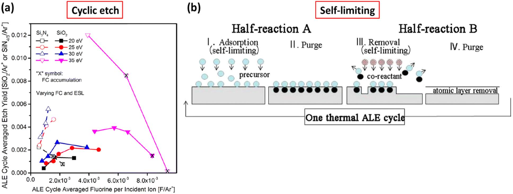
To demonstrate the advantages of ALE in achieving precise, controlled, and uniform etching, we can refer to the synergy between different plasma steps, the self-limiting nature of each etch cycle, and the repetitive cyclic process that collectively enables the production of high-performance devices with nanoscale features. Fig. 5 illustrates three fundamental aspects of ALE: synergy, self-limited etching, and cyclic etch.39 Synergy is demonstrated for the etching of silicon nitride in the combination of hydrogen and fluorinated plasma steps. The initial exposure to hydrogen plasma modifies the silicon nitride surface, making it more reactive to the subsequent fluorinated plasma. This synergistic effect enhances the etch rate and selectivity. The increased etch depth when both plasmas are used sequentially, compared to each plasma used individually, confirms the enhanced efficiency due to synergy.35,39 Self-limited etching is a critical feature of ALE, ensuring that each etch cycle removes only a single atomic layer. Fig. 5(a) shows the average etch yield in ALE at different F/Ar+ ratios, comparing the etching behaviors of Si3N4 and SiO2, which has a significant correlation with cyclic etching. As the F/Ar+ ratio increases, chemical etching efficiency improves, but once the ratio exceeds a critical point, the etch becomes limited by ion bombardment. At high F/Ar+ ratios, fluorocarbon layers accumulate on the surface, leading to a decrease in etch yield, much like the impact of insufficient residue removal between cycles in cyclic etching.40,42,43Fig. 5(b) illustrates the complete cycle of thermal ALE, showing two self-limiting half-reaction processes. In half-reaction A, step I is the adsorption phase, where the precursor self-limits by adsorbing onto the material surface. Once the surface is fully covered, the reaction automatically stops. In half-reaction B, step III is the material removal phase, where the second reactant converts the adsorbed layer into volatile products, removing one atomic layer in a self-limiting manner. This self-limiting characteristic ensures that only one atomic layer is removed per cycle, providing extremely high etching precision.38,41,42 These features ensure high precision, control, and uniformity, which are essential for producing advanced semiconductor devices.
2.3.1.2 Applications of ALE. To evaluate the performance of GaN materials using ALE with Cl2 and either He or Ar plasma, Ruel, Simon, et al. demonstrated that while Ar-based ALE processes show self-limiting behavior and lower damage to GaN, He-based ALE processes lead to deeper ion implantation and higher electrical degradation.44 This research highlights the importance of selecting appropriate etching plasma sources to minimize damage and optimize device performance. Regarding the discussion on optimizing device characteristics using ALE, Du, F, et al. studied the ALE technology and its surface treatment for InAlN/GaN heterostructures. After an appropriate number of ALE etching cycles, the two-dimensional electron gas (2-DEG) density and surface roughness improved by 15% and 11.4%, respectively, compared to using digital etching technology, and the sheet resistance (Rsh) decreased by 6.7%.45
Fig. 6(a) illustrates the high etch selectivity achieved through thermal ALE at 250 °C, demonstrating negligible removal of SiN, SiO2, and TiN after 1000 ALE cycles. This high selectivity is attributed to the targeted chemistry of the process and the absence of energetic ions and radicals, which allows for the precise removal of specific materials without affecting other components in the device.46Fig. 6(b) demonstrates significant benefits of plasma-assisted ALE, including exceptional etch depth uniformity across the wafer and flat silicon etch front, validating its capability to produce atomically smooth surfaces.26
 | ||
| Fig. 6 (a) Example of etch selectivity in thermal ALE at 250 C. Materials are (1) SiN, (2) HfO2, (3) SiO2, (4) TiN, and (5) Al2O3. No measurable removal in SiN, SiO2, and TiN was detected after 1000 ALE cycles.46 (b) Plasma-assisted ALE results showing characteristic ALE benefits with excellent depth uniformity across the wafer and flat silicon etch front on the feature.26 | ||
ALE can provide significant advantages in enhancing normally-off GaN recessed gate MIS-HEMT performance, such as breakdown voltage,47,48 low leakage current,48 and dynamic on-resistance.49 Even the application of ALE for low-damage surface etching of AlGaN has also shown characteristic optimization for high-frequency GaN HEMTs.50 The precision and control capabilities of ALE enable the creation of high-quality interfaces with low surface damage and well-defined features, which are critical for high-power applications.
Fig. 7(a), the cross-sectional image shows the precise etching of AlGaN layers from 25 nm to 3.7 nm. Fig. 7(b) presents the surface roughness measurement that the root mean square roughness (Ra) is 0.4 nm over a 1 μm2 area, indicating the smooth surface achieved through ALE. This smoothness is crucial for minimizing carrier scattering and surface traps and enhancing electron mobility in GaN-based devices.51Table 3 shows the performance of MIS-HEMTs with ALE-fabricated recessed gate devices and demonstrates a competitive balance of high current density (608 mA mm−1), controllable threshold voltage (+2.0 V), and high breakdown voltage (720 V at 1 μA mm−1), making it suitable for high power applications. In comparison, devices fabricated using ICP etching achieve a higher maximum current density of 836 mA mm−1 in double-channel designs but exhibit a lower breakdown voltage (705 V at 1 μA mm−1) and less precise threshold voltage control (+0.5 V). The dynamic on-resistance (Ron,sp) for ALE-fabricated devices is 1.27 mΩ cm2, which is superior to the 1.48 mΩ cm2 observed in ICP-etched devices.
 | ||
| Fig. 7 MIS-HEMT with a recessed gate structure. (a) TEM cross-section image in the gate recess region, highlighting a smoothly etched surface and precise etching control. (b) Surface morphology of the recessed gate region, revealing a surface roughness (Ra) of 0.4 nm, as inspected by AFM.47 | ||
Additionally, ALE-fabricated devices demonstrate significantly reduced surface damage, contributing to enhanced reliability. The smoothness of the etched surface achieved by ALE, characterized by an RMS roughness of 0.4 nm, is markedly better than the 1.2 nm obtained using ICP etching. These quantitative improvements in breakdown voltage (+15 V), threshold voltage stability (+1.5 V), and reduced surface roughness (66.67% improvement) underline the superiority of ALE over ICP etching, particularly for applications requiring precise electrical control and high reliability.51,53
The study by Hwang et al. illustrates the advantages of ALE in achieving low-damage, self-limiting etching processes for AlGaN using O2 and BCl3 plasma.53 This process ensures high etching precision, minimal surface damage, and excellent etch depth control, leading to improved electrical characteristics of Schottky diodes compared to traditional digital etching methods. As shown in Fig. 8(a), the ideality factor was found to be more uniform and lower for diodes fabricated using ALE (approximately 1.0 at a forward voltage of 0.3 V) compared to those made with digital etching (approximately 2.0 at the same voltage). This significant reduction in ideality factor (50% improvement) indicates that ALE causes less plasma-induced damage, resulting in better electrical characteristics, including lower reverse current and higher zero-bias barrier heights.
 | ||
| Fig. 8 (a) Photoluminescence intensity comparison between ALE and digital etching. (b) Ideality factor behavior in the forward voltage region.53 | ||
To further assess the impact on etching damage, photoluminescence (PL) intensity was measured at an etch depth of approximately 5 nm. Fig. 8(b) shows that near-band-edge PL intensity for samples etched using ALE is approximately 30% higher compared to those etched with digital etching. This suggests that ALE produces fewer non-radiative recombination centers, such as nitrogen vacancies, which are responsible for degrading device performance.
NBE is specifically designed to minimize plasma-induced damage on semiconductor materials, particularly GaN-based devices. Conventional plasma etching methods often cause significant surface damage due to ion bombardment, resulting in increased leakage currents, reduced breakdown voltages, and degraded device performance. NBE addresses these issues by providing a damage-free etching environment through the neutralization of ions and reduction of UV photons. This minimizes surface damage and leads to improved electrical characteristics.
Beyond its success with GaN-based devices, NBE has demonstrated significant potential in the fabrication of 3D Fin-FET structures, a cornerstone of modern 3D IC technologies. One of its most critical advantages is its ability to perform selective etching of germanium, a material increasingly used in advanced Fin-FET designs for its superior electron mobility. The neutralization process in NBE minimizes ion bombardment and plasma-induced damage, ensuring precise material removal without affecting adjacent layers. This high selectivity not only preserves the structural integrity of the germanium fins but also maintains clean interfaces,56 which are crucial for achieving high carrier mobility and reliable device performance.
NBE's capabilities in atomic-scale etching and its damage-free nature give it significant potential for fabricating the high-aspect-ratio structures required in Fin-FETs. These characteristics suggest that NBE could become an important tool in 3D IC manufacturing applications.
2.3.2.1 Principles of NBE. NBE operates by utilizing a neutral beam composed of neutralized ions that effectively etch the material surface without the undesirable effects typically associated with conventional plasma etching methods. The NBE system consists of a dual-chamber setup: a plasma generation chamber and an etching chamber, separated by a carbon electrode with high aspect ratio apertures. This configuration allows plasma ions to be neutralized as they pass through the carbon apertures, significantly reducing the presence of charged particles and UV photons. The NBE system, as shown in Fig. 9,54 ensures that the etched surface maintains its integrity and performance, making it crucial for the development of advanced semiconductor devices.
 | ||
| Fig. 9 (a) Neutral beam etching system. (b) Carbon aperture array.54 | ||
The design of the carbon apertures in the NBE system plays a critical role in its effectiveness. The carbon aperture array is crucial for achieving high-efficiency ion neutralization and protecting the substrate during the etching process. Graphite is commonly selected as the aperture material due to its excellent thermal and electrical properties, ensuring durability under intense plasma exposure. The high aspect ratio of these apertures is essential for the neutralization process. As plasma ions generated in the plasma chamber pass through the narrow, elongated carbon apertures, they are neutralized, transforming from charged particles into neutral atoms. This transformation is because neutral atoms, unlike charged ions, do not cause significant damage to the material being etched. The high aspect ratio design also enhances the neutralization process by providing an extended path for ions to interact with the carbon walls, converting charged ions into neutral particles. Moreover, it minimizes energy loss by maintaining the directionality and kinetic energy of neutralized particles while reducing ion-wall collisions.57 Additionally, the high aspect ratio design effectively filters out UV photons, which are another source of damage in conventional plasma etching processes. The carbon aperture array is further engineered to support a pressure differential between the plasma source and the processing regions. This configuration reduces background gas collisions, preserving the energy of the neutral beam and ensuring precise etching performance. By minimizing both ion bombardment and UV photon exposure, the carbon aperture design in NBE significantly reduces surface damage, leading to improved electrical characteristics of the etched devices. This makes NBE particularly advantageous for applications requiring high precision and minimal damage.
2.3.2.2 Applications of NBE. NBE is widely applied in the fabrication of high-density semiconductor devices, including advanced logic and memory devices. Its ability to produce high-resolution patterns with minimal surface damage also makes it suitable for GaN devices used in millimeter-wave applications.58 Additionally, the precise etch depth control and excellent surface roughness for recessed gate E-mode AlGaN/GaN HEMTs exhibit excellent electrical characteristics.59 In addition to its technological advantages, NBE introduces distinct cost implications. While its initial equipment investment is higher due to the neutral beam generation system, it reduces long-term costs by minimizing surface damage and improving process yields. In contrast, traditional plasma etching, with lower upfront costs, often incurs higher operational expenses due to greater defect mitigation needs. These dynamics make NBE ideal for high-precision applications such as GaN-based HEMTs and micro-LEDs,60 where reliability and yield outweigh initial costs. Furthermore, when applied to n-GaN surfaces treated with fluorine ions and neutral beams, NBE optimizes ohmic contacts and exhibits lower contact resistivity. This is because the fluorine neutral beam removes nitrogen from the surface.61 Compared to fluorine ion beams, although both reduce contact resistivity, the fluorine neutral beam is more effective, likely due to the lack of charge-induced defect formation.62 The choice of etching gas in NBE is also a crucial parameter. Ohori, D, et al. studied the etching effects of HBr and Cl2 neutral beams, finding that HBr could achieve a thinner reaction layer than Cl2 because the diameter of Br atoms is 1.2 times larger than that of Cl atoms. Furthermore, HBr could generate less volatile etching products due to the higher boiling point of its byproducts.63
Hemmi et al. demonstrated that adjusting the carbon aperture aspect ratio in NBE significantly affects surface roughness and plasma-induced damage. With a carbon aperture aspect ratio of 10, the RMS roughness was significantly lower at 0.452 nm compared to 1.024 nm for a carbon aperture aspect ratio of 2, highlighting the smoother etch achieved with better neutralization, as shown in Fig. 10. This adjustment in the aperture design effectively reduced surface damage, leading to improved electrical performance in AlGaN/GaN HEMTs.64
 | ||
| Fig. 10 AFM images of the AlGaN surface with different carbon aperture aspect ratio designs.64 | ||
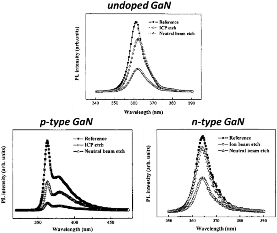
NBE also provides a solution by utilizing a beam of neutral particles that eliminates the charged particles and UV photons responsible for plasma damage.54 This process ensures precise control of etching depth and significantly reduces damage to the etched surfaces. Hemmi et al. demonstrated that NBE-etched GaN HEMTs reduced isolation leakage current by tenfold (1 μA mm−1 to 0.1 μA mm−1 at 4 V) compared to plasma beam (PB) etching, with RMS surface roughness improving from 2.226 nm to 0.427 nm. NBE also increased soft breakdown voltage (SBV) to over 210 V, compared to 25.6 V for PB, and hard breakdown voltage to over 800 V (PB: 600–700 V).54 Furthermore, Park et al., using the PL data shown in Fig. 11, demonstrated a 30% higher near-band-edge PL intensity in NBE-etched GaN, indicating fewer defects and enhanced optical efficiency without an increase in forward voltage.55
 | ||
| Fig. 11 PL data of undoped GaN, p-type GaN, and n-type GaN after etching with ICP and neutral beams, with the reference samples being unetched.55 | ||
Edward Yi Chang et al. demonstrated the superior interface quality and electrical performance of high-frequency GaN HEMTs when utilizing NBE compared to ICP-RIE. High-resolution transmission electron microscopy (HRTEM) images show a smoother and more uniform gate recess interface with NBE, as shown in Fig. 12. The electrical performance, including noise and frequency response, highlights that NBE-processed devices exhibit better direct current (DC) and high-frequency characteristics.58 Compared to ICP-RIE results, on-resistance is improved by 52%, transconductance is increased by 22%, and the noise figure is reduced by 31% using NBE. Additionally, the cutoff frequency is increased by 28%, and drain current density is enhanced. This improvement is attributed to the minimal etching damage provided by the NBE process, making it an excellent technique for high-performance GaN device fabrication.
 | ||
| Fig. 12 HRTEM of the gate recess AlGaN etching region and zoom-in images (a) by neutral beam etching (b) by ICP-RIE.58 | ||
Ray-Hua Horng et al. investigated the performance of NBE and ICP-RIE in the fabrication of GaN-based micro-LEDs. The results shown in Fig. 13(a) and (b), demonstrated that sidewall defects caused by plasma etching are significantly reduced by NBE, thereby enhancing the efficiency of the LEDs. Devices etched with NBE exhibit nearly consistent external quantum efficiency (EQE) across different array sizes, with the EQEmax being 6.95% for 4 × 4 arrays (40 μm) and 7.11% for 2 × 2 arrays (80 μm). In contrast, devices etched with ICP-RIE show a significant decrease in EQE as the size decreases, with EQEmax values of 8.13% for 2 × 2 arrays (80 μm) and 7.48% for 4 × 4 arrays (40 μm). This demonstrates that NBE maintains a more consistent performance, particularly in smaller-sized micro-LEDs, reducing the size effect and enhancing overall device efficiency. Through cathodoluminescence (CL) analysis, as illustrated in Fig. 13(c), it was found that samples etched with NBE have stronger and more sustained radiative recombination signals at the sidewalls, while the signals in ICP-RIE etched samples are weaker and decay more quickly. This indicates that the UV light generated during the ICP-RIE process damages the mesa sidewalls, creating more defects and reducing radiative recombination behavior.65 These findings highlight the significant advantages of NBE technology in fabricating high-performance GaN-based micro-LEDs.
 | ||
| Fig. 13 EQE of micro-LED arrays processed by (a) NBE and (b) ICP-RIE. (c) CL analysis in the blue-light wavelength region: NBE vs. ICP-RIE.65,66 | ||
In this chapter, the application and development of etching techniques, especially dry etching, in semiconductor manufacturing are discussed. The chapter first introduces the basic concepts of conventional etching techniques and compares the advantages and disadvantages of wet etching and dry etching. It then highlights advanced dry etching techniques, including ALE and NBE, which play a crucial role in the fabrication of modern semiconductor devices due to their highly precise control capability. The NBE technique significantly reduces the surface damage during etching by neutralizing the ion beam, which is particularly suitable for GaN-based devices. In this chapter, it is shown how these advanced etching techniques address the limitations of conventional techniques and provide new solutions for fabricating smaller, more efficient and more reliable semiconductor devices.
3. Deposition techniques
Thin film technology is an advanced approach aimed at improving the structural, electrical, magnetic, optical, and mechanical properties of bulk materials. It has found widespread application in semiconductor devices, integrated circuits, transistors, liquid crystal displays, light-emitting diodes, solar cells, sensors, and micro-electromechanical systems (MEMSs).67–69 The distinctive properties of thin film materials are crucial for the technological advancement of various electronic, electrical, magnetic, and optical devices.70,71 These films are created using various physical or chemical methods, each of which is essential for producing ultra-thin materials known for their uniform, conformal, and controllable thickness. As atomic and near-atomic scale manufacturing (ACSM) evolves, the necessity of depositing high-quality, impurity-free thin films for laminated structures becomes crucial.72 This is especially true when film thickness approaches atomic dimensions, posing significant challenges for conventional deposition methods.Traditional thin film deposition processes often face the challenge of achieving a balance between conformality, precise thickness control, and material selection for desired functionality. Fig. 14 shows various types of thin film deposition techniques. Established methods such as physical vapor deposition (PVD) and chemical vapor deposition (CVD), sputtering, spin coating, dip coating, and spray pyrolysis have been extensively utilized. However, achieving conformal film deposition over complex three-dimensional structures with high aspect ratios is challenging for techniques such as PVD, and electrodeposition is limited to conductive materials only. Although CVD is adaptable and can produce high-quality films, it has drawbacks, including high processing temperatures and the difficulty of obtaining consistent thickness on complex geometries.
 | ||
| Fig. 14 Thin film deposition techniques. | ||
Recently, an advanced vapor-phase deposition process known as ALD has addressed these limitations by providing precise control over film thickness and conformality due to its self-limiting surface reactions. This novel technique has been extensively investigated, effectively satisfying the urgent demand in advanced micro/nano semiconductor manufacturing.73,74 The fundamental advantages of this technology were compared to those of other deposition methods such as electroplating, spin coating, sputtering, PVD, and CVD. It has the potential to overcome current challenges and establish new standards at the atomic level in thin film technology.
3.1 Traditional deposition technology
Thin film deposition techniques are systematically classified into four distinct categories based on the nature of the deposition process, as illustrated in Fig. 14. This classification fundamentally relies on whether the deposition mechanism in PVD or CVD is primarily physical or chemical. Additionally, solution deposition thin film methods include a variety of techniques, including chemical bath deposition (CBD),75,76 spray pyrolysis,77 sol–gel processing,78 spin coating,79 and dip-coating.80 Each method utilizes chemical reactions in a solution to form films. The key parameters that must be carefully controlled in these chemical reactions include solution concentration, temperature, pH levels, and reaction time. Precise control of these factors is important to achieve the desired film properties and ensure that the film is suitable for a specific application. In contrast, physical processes such as PVD,81 sputtering,82 molecular beam epitaxy (MBE),83 electron beam evaporation,84 and thermal evaporation primarily rely on the physical transfer of a material from a source to the substrate under vacuum conditions. The chemical category includes methods such as CVD,85 plasma-enhanced CVD (PECVD),86 metal–organic CVD (MOCVD),87 and ALD,88 which involve chemical reactions at the surface of the substrate to grow the film. Finally, the classification of other CVD techniques includes advanced methods such as mist-CVD and hydride vapor phase epitaxy (HVPE). Mist-CVD operates without vacuum environments, utilizing aerosolized precursors for efficient deposition, making it ideal for large-area applications. This technique has been effectively employed to grow high-quality Ga2O3 films, demonstrating advantages such as low cost, simplicity, and compatibility with various substrates. For example, high-quality crystalline NiO/β-Ga2O3 p–n heterojunctions grown via mist-CVD exhibit excellent crystallinity, showcasing its potential for advanced semiconductor device applications.89,90 HVPE, on the other hand, is primarily employed for high-quality single-crystal growth, particularly in III–V semiconductors. Additionally, HVPE has been effectively utilized in depositing aluminum nitride (AlN), a material renowned for its wide bandgap and high thermal conductivity. HVPE-grown AlN films exhibit excellent structural properties, including high crystallinity and smooth surface morphology, which are critical for applications requiring high breakdown voltages and large-area substrates. Furthermore, HVPE facilitates the growth of thick AlN layers at high growth rates, enabling the production of free-standing AlN wafers that serve as substrates for III-nitride device structures. These advancements underscore the versatility of HVPE in supporting advanced semiconductor applications, such as deep ultraviolet optoelectronics and acoustic devices.91 These advanced methods expand the scope of CVD techniques by offering unique advantages such as cost-effectiveness, compatibility with diverse substrates, and high crystal quality, catering to the demands of next-generation electronic and optoelectronic devices.Each thin film deposition technology has unique advantages and inherent limitations, which greatly affect their application in various technical fields. PVD processes, such as sputtering and evaporation, offer excellent control over film purity and composition due to their vacuum-based deposition environment, facilitating the production of high-quality films with precise microstructural characteristics. Nevertheless, there are process challenges, including limitations in material selection, difficulties in achieving conformal coverage over complex geometries, and potential issues with film quality. Conversely, CVD processes are often preferred for their ability to produce uniform coatings over large and intricately shaped areas, a capability that PVD cannot consistently achieve. The capability of CVD to handle a wide range of materials, combined with its effectiveness in filling high aspect ratio structures, renders it essential for the fabrication of semiconductor devices and integrated circuits.92 However, CVD methods typically require higher substrate temperatures and may introduce unnecessary impurities from precursor chemicals, which creates challenges related to thermal budget and material compatibility.
Among these traditional methods, ALD emerges as a particularly promising technology. The unique nature of ALD enables high uniformity and easy control over composition and stacking processes.93 Recently, there has been increased interest in the fabrication process for each layer, driven by the need for continuously scaled-down devices. ALD operates on the principle of sequential self-limiting surface reactions, enabling atomic-scale control over film thickness and composition.94 This unique feature allows for the deposition of extremely thin and conformal films, which are essential for advanced semiconductor applications where dimensional control is critical. Additionally, ALD provides superior uniformity when deposited on high aspect ratio structures, overcoming one of the major limitations faced by PVD and CVD.95 Despite its slower deposition rates, the precision and scalability of ALD position it as a key technology in the ongoing development of nano-scale devices and structures, highlighting its potential to drive future innovations in thin film technology.96 A comprehensive comparison of CVD, PVD, and ALD is shown in Table 4.
| Property | PVD | CVD | ALD |
|---|---|---|---|
| Growth mechanism | Continuous | Continuous | Self-limiting |
| Growth rate | 100 nm–1 μm min−1 | 10–100 nm min−1 | 0.1–1 nm min−1 |
| Materials | Metals, elements, alloys, and some oxides/nitrides | Oxides, nitrides, sulfides, and metals, elements | Oxides, nitrides, sulfides, and metals, elements |
| Temperature range | 20–500 °C | 200–1000 °C | 50–300 °C |
| Vacuum | 10−6–10−3 torr | 10−3–10 torr | 10−2–10 torr |
| Directionality | Line-of-sight | Isotropic | Isotropic |
| Cleanliness | Particles | Particles | No particles |
| Conformality | 50–70% | 70–90% | >90% |
| Uniformity | ∼80 Å range | ∼10 Å range | Å range |
3.2 Atomic layer deposition
Originally developed and globally recognized as atomic layer epitaxy in the late 1970s, ALD was initially motivated by the need to create thin-film electroluminescent (TFEL) flat-panel displays.97 These displays require high-quality dielectric and luminescent films on large-area substrates. By the mid-1980s, the utility of ALD was extended to epitaxial compound semiconductors. Significant research efforts in the late 1980s focused on the preparation of III–V compounds. The renewed focus on ALD during the mid-1990s was driven by its applications in silicon-based microelectronics. The continuous miniaturization of device dimensions and the increasing aspect ratios in integrated circuits demand the adoption of novel materials and deposition techniques. ALD is regarded as one of the most promising methods, owing to its ability to produce ultrathin, conformal films with precise atomic-level control over film thickness and composition. This section will further explore the ALD mechanism, area-selective atomic layer deposition (AS-ALD), and its applications in further detail.Fig. 15(a) presents a schematic comparison of a sputtering system and an ALD system, highlighting the differences in film deposition morphology on high-aspect-ratio devices. Fig. 15(b) illustrates the general ALD process through cyclic surface reactions: (1) adsorption of precursor A, (2) purging with inert gas to remove excess precursors and byproducts, (3) adsorption of precursor B, and (4) repeated purging to facilitate layer-by-layer growth until the desired film thickness is achieved.99 This adsorption process involves both physisorption and chemisorption, with excess physisorbed materials that can be removed by purging with an inert gas. The limitation of active surface sites ensures that the surface reactions of each cycle are self-limiting. Due to its self-limiting characteristics, ALD can precisely control film thickness at the atomic level by adjusting the number of growth cycles. The saturation process during each cycle restricts the reaction to less than one atomic or molecular layer, promoting uniformity and excellent step coverage across complex surfaces and large areas. ALD flexibility covers a wide range of materials, allowing the deposition of oxides, nitrides, fluorides, sulfides, metals, polymers, and mixed or doped materials.101 It also supports the deposition of multilayers with customizable properties at the atomic level, expanding the scope of its applications. Notably, materials such as Al2O3, TiO2, and TiN can be deposited at temperatures below 150 °C, reducing the risk of thermal damage to temperature-sensitive substrates.99
 | ||
| Fig. 15 Schematic illustrations of thin film deposition techniques. (a) Comparison of PVD and ALD on structured surfaces, highlighting the limitations of PVD in high aspect ratio devices and the conformality of ALD.96 (b) Diagram of the ALD process showing the layer-by-layer deposition of Al2O3 from TMA and H2O precursors.99 (c) ALD growth rate graph as a function of deposition temperature, illustrating the temperature sensitivity and optimal ranges for precursors.100 | ||
Despite its advantages, ALD may exhibit undesirable side reactions, present challenges due to its complex reaction chemistry and reactor design, and generally offer low throughput and potential issues with conformality.102 To address the issue of low throughput, strategies such as spatial ALD and plasma-enhanced ALD (PE-ALD) have been developed. Spatial ALD increases deposition rates by simultaneously allowing continuous precursor exposure across different substrate regions, thereby bypassing ALD's traditional cyclic nature.74 In contrast, PE-ALD utilizes plasma to activate surface reactions, enabling faster deposition rates and facilitating deposition on less reactive surfaces at lower temperatures.103 While these methods enhance throughput, they also introduce challenges, including higher equipment costs and increased process complexity, which must be considered for industrial applications. In general, the temperature of the process is crucial for ALD reactions. ALD must operate within a specific temperature range to avoid slow growth rates, thermal disintegration, and slow reaction of precursors. The “temperature window” is defined as the range within which film growth reaches saturation, as illustrated in Fig. 15(c). At temperatures below this window, reactions may be lacking or may lead to precursor condensation, while at higher temperatures, the risk of precursor desorption or thermal decomposition increases. Hence, maintaining conditions within the ALD temperature window is crucial for optimizing the deposition process.
As research continues to expand the capabilities and address the limitations of ALD, this technique remains at the leading edge of thin film deposition technologies, promising further enhancements and wider applications in the future. This progress is essential for meeting the evolving demands of nano-engineering and microelectronics, where the atomic-level control provided by ALD is increasingly critical.
 | ||
| Fig. 16 Detailed representations of AS-ALD techniques and analyses. (a) Schematic illustration of the AS-ALD process, showcasing the method for selective area deposition.104 (b) Integration of isothermal atomic layer deposition with atomic layer etching supercycles for selective deposition of TiO2 on SiO2, complemented by TOF-SIMS images of the TiO2 on the patterned structure.105 (c) XPS depth profiles for ALD HZO films grown at 280 °C on Ru and TiN substrates after 200 and 300 cycles.106 (d) TEM images and EDX mapping of ZnO crystals coated with 21 nm of amorphous TiN after 300 cycles of the PE-ALD process, revealing variations in particle size and shape and the composition mapping performed with HAADF-STEM.107 | ||
Selectivity is determined not only by film thickness but it also serves as a key indicator of process efficiency. As the growth phase exceeded the defined selective window, deposition began on the non-growth regions, resulting in reduced selectivity.104 An additional etching step can be integrated into the conventional binary ALD cycle to address this issue.105 This step is crucial for removing nuclei in non-growth areas, thereby preserving high selectivity. Importantly, the etching process must be selectively defined to remove the deposited material without affecting the integrity of the underlying substrate. This approach ensures the precision and effectiveness of the ALD technique in applications that require high pattern accuracy. For example, the selective deposition of TiO2 thin films on Si/SiO2-patterned surfaces, as shown in Fig. 16(b).105 The implementation of supercycles enabled the deposition of TiO2 films with a thickness exceeding 12 nm while still maintaining a high selectivity of 97%. This study demonstrated the advanced capabilities of selective deposition techniques, including ALD and ALE, among other self-limiting reaction processes. The findings make a substantial contribution to the understanding of how complex atomic-scale structures can be engineered with precise material deposition, thereby enhancing the potential applications of these technologies in semiconductor manufacturing and other fields.
Kim et al. further advanced AS-ALD by developing a method for selectively depositing Hf1−xZrxO2 (HZO) thin films through the catalytic dissociation of O2 molecules.106 This significantly enhanced the dielectric constants on metal substrates, achieving high dielectric constants of 34 on Ru and 31 on TiN substrates. Fig. 16(c) illustrates XPS depth profiling, confirming the selective nature and purity of the deposited films. This study emphasizes the potential of catalytic local activation to advance three-dimensional nanopatterning in nanoelectronic device fabrication. Moreover, Longrie et al.'s study utilized a rotary reactor to deposit TiN on submicrometer ZnO powder through both thermal and PE-ALD.107 This method proved effective in completely removing N(CH3)2 ligands. Fig. 16(d) displays energy-dispersive X-ray spectroscopy (EDX) mapping and transmission electron microscopy (TEM) images that confirmed uniform coatings on all powder agglomerates and individual particles. Their findings revealed that the plasma-enhanced layers contained higher titanium and nitrogen content with significantly reduced oxygen and carbon levels compared to thermally grown films, indicating improved compositional purity. These studies collectively highlight the effectiveness of AS-ALD in achieving precise and selective thin-film deposition, which is critical for the ongoing development of nanoscale device fabrication. These findings explore their implications for the future of semiconductor manufacturing, reflecting on how AS-ALD can address the growing complexity and stringent requirements of modern electronic devices.
3.2.3.1 ALD in optoelectronics applications. As the size of LEDs decreases, the impact of sidewall defects becomes more significant, resulting in reduced wafer luminous efficiency.113 ALD has become an important technology for improving the performance of LED devices, especially for passivation applications. Sidewall passivation minimizes surface recombination velocities, which can greatly affect the efficiency and performance of LEDs.114 A red micro-LED with SiO2 by ALD used as a sidewall passivation layer is schematically shown in Fig. 17(a).115 ALD offers superior coverage and conformality so that even the most complex microstructures in LED devices are effectively passivated, reducing non-radiative recombination at the sidewalls. From the comparison between devices with various coatings and different current levels, a significant decrease in integrated optical power can be observed as shown in Fig. 17(b). For smaller devices, such as those with dimensions of 5 μm and 15 μm, ALD technology demonstrated lower leakage currents and higher conductivity compared to PECVD. Specifically, in larger devices with a size of 50 μm, ALD-coated samples exhibited an average reduction in leakage current by a factor of 7.8, indicating that ALD is more effective in sidewall passivation, thereby minimizing leakage pathways and surface recombination losses. When examining micro-LEDs of various sizes, the significance of ALD sidewall treatment becomes even more apparent. This significant difference is primarily attributed to increased surface recombination in smaller devices.115 Micro-LEDs with ALD sidewall passivation demonstrate significantly higher output power densities and external quantum efficiencies (EQEs) compared to those without ALD treatment, as illustrated in Fig. 17(c). The enhancement in EQE of micro-LEDs with ALD sidewall passivation is primarily due to the reduction in Shockley–Read–Hall (SRH) non-radiative recombination. The ALD treatment improves surface quality by passivating defects and reducing surface states, which are significant contributors to non-radiative recombination, particularly in smaller devices. This leads to more efficient carrier recombination and higher light output. The uniform passivation provided by ALD reduces surface states and defects, which are more pronounced in smaller devices due to their higher surface-to-volume ratios.116 Consequently, micro-LEDs treated with ALD maintain higher efficiency and brightness, which is crucial for applications that require high-resolution displays and precise lighting control. Specifically, the ALD-treated devices show a significant improvement in surface recombination velocity, reducing it from 1026 cm s−1 to 551.3 cm s−1, which translates into a 73.47% enhancement in EQE for 5 μm devices and 66.72% for 10 μm devices.
 | ||
| Fig. 17 Applications of ALD in LED enhancement. (a) Schematic diagram of a red micro-LED with an ALD-applied SiO2 sidewall passivation layer.115 (b) Integrated spectral intensities for samples treated with ALD and PECVD at high/low current densities.115 (c) Output power density comparisons for micro-LEDs of dimensions 5 × 5 μm2 and 10 × 10 μm2, with and without ALD sidewall treatments, including peak EQE.116 (d) Comparison of emission lifetimes in OLED panels with and without Al2O3 ALD encapsulation, illustrating the durability advantages of ALD.117 | ||
Furthermore, ALD offers substantial advantages in the passivation and encapsulation of LED and OLED devices. Its ability to produce high-quality, conformal films ensures enhanced current densities, output power, and EQE in micro-LEDs, as well as extended emission lifetimes in OLED panels, as shown in Fig. 17(d). The EQE enhancement for micro-LEDs treated with ALD sidewall passivation was significant, with improvements of up to 73.47% for 5 μm devices and 66.72% for 10 μm devices. Additionally, ALD-treated OLED panels showed little to no degradation in luminance intensity over extended periods, demonstrating the effectiveness of ALD in maintaining device performance.117
3.2.3.2 ALD in microelectronics and semiconductor applications. As device dimensions decrease, conventional materials and fabrication methods encounter limitations, necessitating the development of advanced solutions such as ALD. In the case of FinFETs, a 3D gate is used to replace planar grids, improving device density and performance, as presented in Fig. 18(a). ALD enables the uniform coating of advanced 3D gate structures with high-k dielectrics such as HfO2, achieving an equivalent oxide thickness (EOT) of around 1 nm.121 This results in a reduction of leakage current density from approximately 10−6 A cm−2 to 10−9 A cm−2 and an 85% retention of universal SiO2 mobility, significantly enhancing gate control, reducing leakage, and improving overall efficiency and scalability. Additionally, the stability of threshold voltage under stress conditions is maintained within ±5%, ensuring reliable device operation.
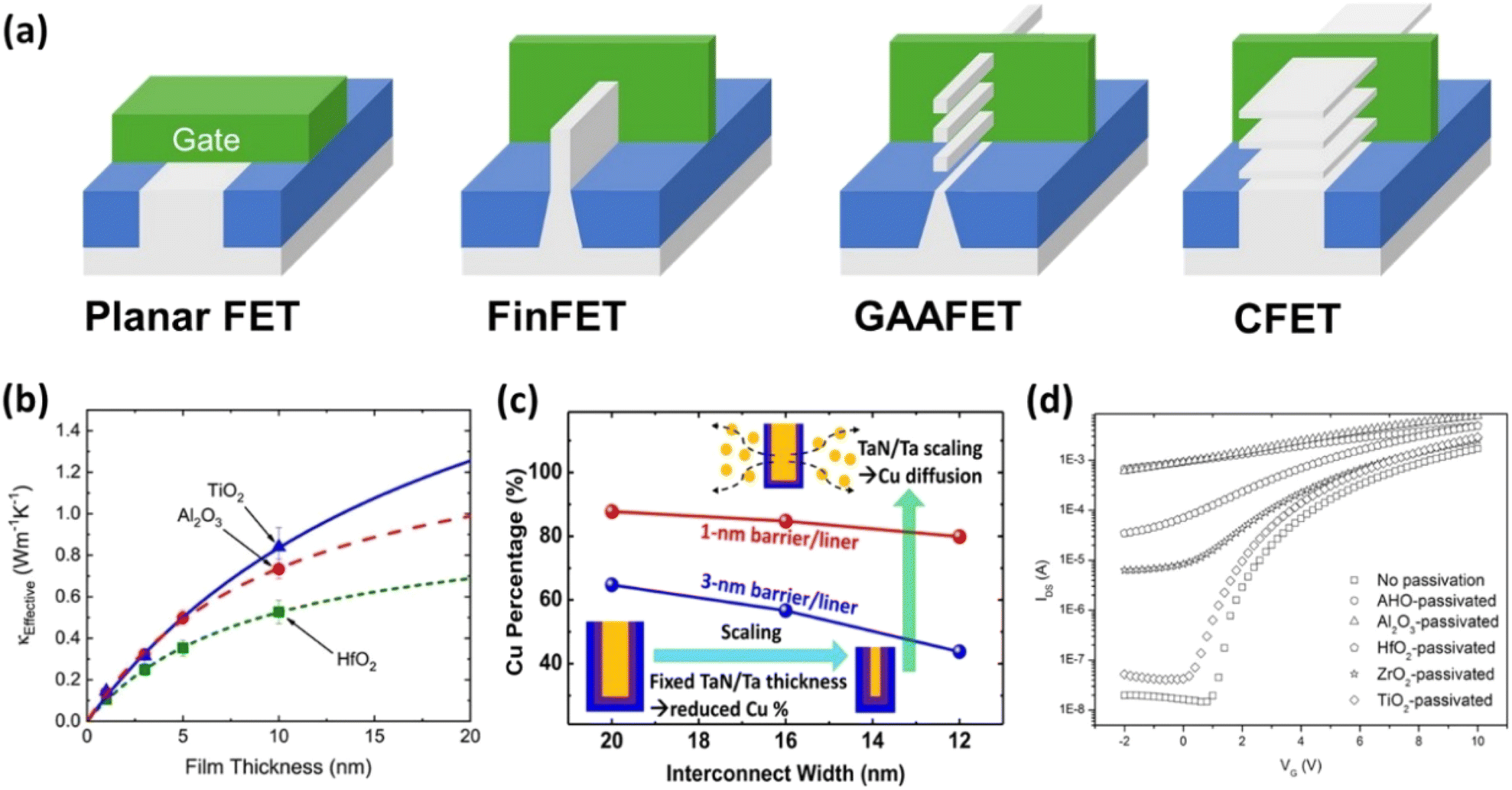 | ||
| Fig. 18 Applications of ALD in microelectronics and semiconductors. (a) Evolution of transistor design concepts from planar to CFET structures. (b) The fabrication of flexible ZnO thin-film transistors on plastic substrates using a low-temperature ALD process.118 (c) The qualifying criteria for barrier and liner layers.119 (d) Transfer characteristics of the ZnO TFTs before and after being passivated with various ALD films.120 | ||
In the field of microelectronics and semiconductors, ALD is pivotal for depositing high-k dielectric materials such as hafnium oxide (HfO2) and aluminum oxide (Al2O3). These high-k materials are characterized by their ability to provide higher capacitance densities compared to traditional silicon dioxide, which is essential for scaling down transistor sizes without increasing leakage currents.122 Specifically, HfO2 and Al2O3 exhibit excellent insulating properties, with a high-k, which enhances gate capacitance while maintaining low equivalent oxide thickness.123 This results in improved gate control and reduced power consumption in transistors. Moreover, their thermal stability and compatibility with silicon processes make them ideal for use in advanced semiconductor devices.124Fig. 18(b) illustrates the effective thermal conductivity of Al2O3, HfO2, and TiO2 films with varying thicknesses between 1 and 10 nm, demonstrating their ability to maintain insulating properties across different scales, further contributing to reduced leakage currents and enhanced transistor performance.118 These high-k materials replace traditional silicon dioxide, reducing gate leakage currents and enhancing capacitance, thereby maintaining device performance at smaller scales.
In advanced memory devices such as dynamic random-access memory (DRAM) and NAND flash, the requirement for uniform trench structures and precise capacitor fabrication is critical. For DRAM capacitors, ALD is essential for depositing ultra-thin, conformal layers of HfO2, which increases capacitance density by up to 30% while reducing leakage currents to 10−9 A cm−2. In NAND flash, ALD ensures uniform oxide–nitride–oxide (ONO) stack deposition, which significantly enhances memory retention and reliability, particularly in high-temperature environments. ALE further improves trench profiles, achieving sidewall smoothness within 1 nm, essential for minimizing variability in memory cell performance.125 ALD facilitates the deposition of high-k materials with exceptional uniformity, achieving a 20–30% increase in memory density and reducing leakage currents to levels below 10−8 A cm−2. ALE complements this process by creating precise trenches with minimal variability. Trenches fabricated via ALE exhibit depth uniformity exceeding 98%, which ensures consistent electrical performance and enhances capacitor reliability. Furthermore, ALD plays a crucial role in the formation of metal gate electrodes. This transition from polysilicon gates to metal gates is essential for reducing gate resistance and enhancing transistor speed. Materials such as titanium nitride (TiN) and tantalum nitride (TaN), deposited via ALD, ensure uniform coverage over complex 3D structures, such as the fin structures in FinFETs.126 This uniformity forms effective gate electrodes that reduce the gate resistance and thus improve the overall speed and efficiency of the transistor.
In integrated circuits, ALD is vital for creating effective barrier and liner layers for copper interconnects, preventing copper diffusion into surrounding materials, which is critical for circuit reliability.119,127Fig. 18(c) summarizes the qualifying criteria for barrier and liner layers, as well as process-related issues affecting surrounding materials and structures. By reducing barrier/liner thickness to sub-nanometer levels, ALD enables a 15% increase in copper volume, thereby lowering line resistance and improving conductivity. Devices utilizing ALD-deposited barrier layers demonstrate a 25% reduction in leakage current, enhancing reliability and scalability for advanced nodes.
The conformity in high aspect ratio features is crucial for the integrity of these interconnects, and ALD's precision is particularly effective here. For instance, ALD's application in depositing semiconductor materials such as indium gallium zinc oxide (IGZO) for thin-film transistors (TFTs) enables significant improvements in device performance.128 IGZO deposited via ALD achieves higher electron mobility, typically exceeding 10 cm2 V−1 s−1, compared to traditional amorphous silicon TFTs, which generally exhibit mobilities around 1 cm2 V−1 s−1.129 This increase in mobility directly enhances the switching speed and overall performance of advanced display technologies. The uniform deposition capability of ALD ensures consistent electrical properties across large areas and complex structures, which is critical for the development of flexible and large-area electronics. Furthermore, ALD's low-temperature deposition, often below 200 °C, preserves the integrity of flexible and wearable electronics by preventing damage to sensitive substrates, which might occur at higher temperatures.130 For example, ZnO TFTs fabricated on plastic substrates using low-temperature ALD show high transparency (over 85%) and robust electrical performance, with on/off ratios exceeding 106, as illustrated in Fig. 18(d). This capability underscores ALD's potential in advancing high-performance, flexible electronic devices by maintaining material properties while ensuring mechanical flexibility.120
Overall, the role of ALD in semiconductor fabrication is expected to grow as the demand for smaller, more efficient electronic devices increases. ALD's ability to deposit thin, uniform films with precise control over composition and thickness makes it an essential tool for ongoing innovations in semiconductor technology. Emerging applications, such as 3D ICs and advanced memory devices, also benefit from ALD's precision and uniformity.131 In summary, ALD plays a crucial role in the advancement of transistor technology. For example, ALD ensures conformal coating of TSVs, achieving a 95% improvement in vertical integration efficiency, while ALE provides precise etching with minimal sidewall damage. These advancements support the ongoing miniaturization and diversification of electronic devices. In 3D ICs, ALD enables the deposition of high-k dielectrics for TSV insulation, achieving leakage current reductions to levels below 10−8 A cm−2 and ensuring consistent capacitance values across high-aspect-ratio structures.132 This capability enhances the reliability of interconnects, reducing failure rates by over 20%. Additionally, ALE's atomic-scale precision allows for the etching of TSVs with depth uniformity exceeding 98%, critical for maintaining signal integrity in multi-layer chip designs.
3.2.3.3 ALD in environmental and energy domains. In addition to the applications mentioned above, ALD is highly effective for depositing functional layers on specific surfaces. In photovoltaics, ALD enhances solar cell performance and durability by reducing surface recombination through passivation layers at rear silicon surfaces. Typically made of Al2O3 or TiO2, these layers decrease surface recombination velocities and increase efficiency, as shown in Fig. 19(a).133 The incorporation of an ultrathin Al2O3 layer at the perovskite/PEDOT interface resulted in an increase in power conversion efficiency from 9.6% to 11.2%. This enhancement is attributed to a reduction in charge recombination and improved passivation provided by the ALD layer. Additionally, the ALD-treated devices exhibited an increase in open-circuit voltage from 0.85 V to 0.91 V and an improvement in the fill factor from 0.59 to 0.65. The passivation mechanism involves chemical passivation, which reduces surface defect states, and field-effect passivation, which repels charge carriers away from the surface.137,138 For example, Al2O3 layers introduce negative fixed charges that repel electrons, thereby reducing electron–hole recombination. ALD is also utilized in thin-film and perovskite solar cells to achieve precise control over layer thickness and composition, optimizing device architecture and stability. This uniformity is essential for maintaining the structural and functional integrity of solar cells under environmental stressors such as moisture and temperature variations.
 | ||
| Fig. 19 Applications of ALD in environmental and energy domains. (a) Passivation layers of Al2O3 deposited via ALD in perovskite solar cells.133J–V curves of the champion perovskite devices with and without the ALD Al2O3 layer at the perovskite/PEDOT interface, along with stabilized power output (SPO) measurements of the respective devices. (b) The schematic illustration of synthesis of a single-atom Pd/graphene catalyst via ALD.134 (c) ALD is utilized to fabricate core/shell structures in drug delivery systems, establishing a correlation between the fine particle fraction and interparticle force following extended storage.135 (d) ALD coatings can protect Fe3O4 nanoparticles from oxidation and provide a controlled surface for functionalization.136 | ||
Catalysis is another area where ALD has made substantial contributions. ALD enables the deposition of catalytic materials with atomic precision, facilitating the creation of highly active and stable catalysts. For instance, ALD can be used to deposit noble metal nanoparticles, such as platinum or palladium, on high-surface-area supports, resulting in catalysts with a high dispersion of active sites essential for catalytic reactions.112 A notable example involves the fabrication of atomically dispersed Pd on graphene using ALD, as illustrated in Fig. 19(b). In the selective hydrogenation of 1,3-butadiene, the single-atom Pd1/graphene catalyst demonstrated approximately 100% butene at 95% conversion.134 The high performance is attributed to changes in the adsorption mode of 1,3-butadiene and the enhanced steric effect on the isolated Pd atoms. Furthermore, ALD allows for the engineering of core–shell structures, enhancing catalytic activity and selectivity, while also improving stability and resistance to sintering and poisoning.139 These attributes are particularly valuable in applications such as automotive exhaust treatment, hydrogen production, and chemical synthesis.
In the field of biomedicine, ALD's precise control over film properties has been harnessed for a variety of applications. One prominent example is the use of ALD to create biocompatible coatings for medical implants.140 These coatings, often made of materials such as titanium dioxide or hydroxyapatite, enhance the integration of implants with biological tissues, reduce the risk of infection, and improve the overall biocompatibility of the device. Additionally, ALD is utilized in the development of drug delivery systems. The as-deposited ceramic films exhibited no cytotoxicity in the human cell culture environment. By coating nanoparticles with ALD films, it is possible to precisely control the release rates of therapeutic agents, enhance the stability of the drug formulations, and target specific tissues or cells. Fig. 19(c) displays the implementation of ceramic ALD films such as SiO2, TiO2, and Al2O3, which significantly increased the fine particle fraction of budesonide.135 In the study, the implementation of ceramic ALD films such as SiO2, TiO2, and Al2O3 on budesonide particles significantly increased the fine particle fraction (FPF) by approximately 2.3 times for SiO2 and Al2O3 and 1.9 times for TiO2, after 10 ALD cycles. This indicates high drug loading and improved cell viability. This precision is crucial for maximizing the therapeutic efficacy while minimizing side effects. Moreover, magnetic nanoparticles show promise in magnetic resonance imaging, hyperthermia treatment, and targeted drug delivery, as depicted in Fig. 19(d). The enhanced stability and biocompatibility provided by ALD coatings make these magnetic nanoparticles more effective for clinical applications.
In addition to its applications in LEDs, transistors, photovoltaics, catalysis, and biomedicine, ALD is also crucial in other fields such as energy storage and environmental protection. For energy storage, ALD improves battery electrodes and electrolyte interfaces, resulting in increased capacity, stability, and lifespan in lithium-ion batteries. In environmental protection, ALD is utilized to create advanced materials for gas separation and water purification, offering solutions for cleaner air and water. The precision and versatility of ALD enable it to address complex challenges across these diverse fields.
In this chapter, the application of thin-film deposition techniques, in particular ALD, to the fabrication of modern semiconductors is explored in depth, as ALD stands out for its ability to precisely control the thickness and composition of thin films at the atomic level and has become a key method for realizing high-performance and high-reliability device fabrication. The principles of ALD, the development of AS-ALD, and its wide range of applications in optoelectronics, semiconductors, and energy technologies are described in detail, showing unparalleled advantages in increasing the efficiency of optoelectronic devices, optimizing high-k dielectric layers and metal gate electrodes, and improving the performance of batteries and fuel cells. Overall, this chapter demonstrates ALD as an advanced method in current thin-film deposition techniques, whose remarkable versatility and precision have led to its expanding range of applications in modern technology.
4. Conclusions
The future of ALD, ALE, and NBE technologies is promising as ongoing advancements continue to address the evolving demands of semiconductor manufacturing. Numerous optimization strategies have been employed to enhance their precision and efficiency. In particular, controlling deposition thickness in ALD, achieving atomic-level etching with ALE, and minimizing surface damage through NBE have proven crucial for improving device performance. Geometrical parameters such as layer thickness, etch depth, and surface passivation have significant impacts on device reliability and durability. Addressing thermal management, particularly in high-power applications, becomes essential as devices scale further. Future efforts could explore the use of more thermally conductive substrates and the refinement of etching profiles to minimize defects and improve device performance. Additionally, optimizing contact technologies to reduce resistance and ensure smooth surface morphology will be critical. Looking ahead, further research should focus on enhancing the uniformity and precision of these processes for advanced applications in micro-LEDs, high-speed communications, and optoelectronics. Future research should consider the performance capabilities of ALD, ALE, and NBE technologies to promote the development of next-generation semiconductor devices.Data availability
No new data were generated or analysed in the course of this study. This review is based on previously published data, which are fully cited in the manuscript.Conflicts of interest
There are no conflicts to declare.References
- T. Wei, Z. Han, X. Zhong, Q. Xiao, T. Liu and D. Xiang, iScience, 2022, 25, 105160 CrossRef CAS PubMed.
- R. D. Miller, Science, 1999, 286, 421–423 CrossRef CAS.
- M. Krishnan and M. Lofaro, in Advances in Chemical Mechanical Planarization (CMP), Elsevier, 2016, pp. 27–46 Search PubMed.
- S. Wang, Y. Sun, F. Dong, L. Xue, R. Li, C. Sheng and S. Liu, In 2021 IEEE 23rd Electronics Packaging Technology Conference (EPTC), 2021, pp. 524–529 Search PubMed.
- D. M. Fleetwood, IEEE Trans. Nucl. Sci., 2021, 68, 509–545 CAS.
- Y. Zhang, A. Zubair, Z. Liu, M. Xiao, J. Perozek, Y. Ma and T. Palacios, Semicond. Sci. Technol., 2021, 36, 054001 CrossRef CAS.
- H. Chiang, T. Chen, J. Wang, S. Mukhopadhyay, W. Lee, C. Chen, W. Khwa, B. Pulicherla, P. Liao and K. Su, In 2020 IEEE Symposium on VLSI Technology, 2020, pp. 1–2 Search PubMed.
- A. K. Gundu and V. Kursun, IEEE Trans. Electron Devices, 2022, 69, 922–929 CAS.
- H. Abe, M. Yoneda and N. Fujiwara, Jpn. J. Appl. Phys., 2008, 47, 1435 Search PubMed.
- M. Shearn, X. Sun, M. D. Henry, A. Yariv and A. Scherer, Semicond. Technol., 2010, 27, 81–105 Search PubMed.
- K. Nojiri, Dry Etching Technology for Semiconductors, Springer, 2015 Search PubMed.
- B. Wu, A. Kumar and S. Pamarthy, J. Appl. Phys., 2010, 108, 051101 CrossRef.
- K. Racka-Szmidt, B. Stonio, J. Żelazko, M. Filipiak and M. Sochacki, Materials, 2021, 15, 123 Search PubMed.
- D. Zhuang and J. Edgar, Mater. Sci. Eng., R, 2005, 48, 1–46 CrossRef.
- J. L. Weyher and J. J. Kelly, Springer Handbook of Crystal Growth, 2010, 1453–1476 Search PubMed.
- J. Weyher, P. Brown, J. Rouviere, T. Wosinski, A. Zauner and I. Grzegory, J. Cryst. Growth, 2000, 210, 151–156 Search PubMed.
- B. Ozdemir, M. Kulakci, R. Turan and H. E. Unalan, Nanotechnology, 2011, 22, 155606 CrossRef PubMed.
- M. Theunissen, J. Appels and W. Verkuylen, J. Electrochem. Soc., 1970, 117, 959 CrossRef CAS.
- P. A. Kohl, IBM J. Res. Dev., 1998, 42, 629–638 CAS.
- S. Randolph, J. Fowlkes and P. Rack, Crit. Rev. Solid State Mater. Sci., 2006, 31, 55–89 CrossRef CAS.
- P. G. Glöersen, J. Vac. Sci. Technol., 1975, 12, 28–35 CrossRef.
- R. Shul, G. McClellan, S. Casalnuovo, D. Rieger, S. Pearton, C. Constantine, C. Barratt, R. Karlicek, C. Tran and M. Schurman, Appl. Phys. Lett., 1996, 69, 1119–1121 CrossRef CAS.
- H. Jansen, H. Gardeniers, M. de Boer, M. Elwenspoek and J. Fluitman, J. Micromech. Microeng., 1996, 6, 14 CrossRef CAS.
- C. Cardinaud, M.-C. Peignon and P.-Y. Tessier, Appl. Surf. Sci., 2000, 164, 72–83 Search PubMed.
- F. Houle, Appl. Phys. A: Mater. Sci. Process., 1986, 41, 315–330 Search PubMed.
- K. J. Kanarik, T. Lill, E. A. Hudson, S. Sriraman, S. Tan, J. Marks, V. Vahedi and R. A. Gottscho, J. Vac. Sci. Technol., A, 2015, 33, 020802 Search PubMed.
- K. Endo, S. Noda, M. Masahara, T. Kubota, T. Ozaki, S. Samukawa, Y. Liu, K. Ishii, Y. Ishikawa and E. Sugimata, IEEE Trans. Electron Devices, 2006, 53, 1826–1833 CAS.
- W. Lu, Y. Lee, J. Murdzek, J. Gertsch, A. Vardi, L. Kong, S. M. George and J. A. del Alamo, In 2018 IEEE International Electron Devices Meeting (IEDM), 2018, p. 39 Search PubMed.
- K. Ishikawa, K. Karahashi, T. Ishijima, S. I. Cho, S. Elliott, D. Hausmann, D. Mocuta, A. Wilson and K. Kinoshita, Jpn. J. Appl. Phys., 2018, 57, 06JA01 Search PubMed.
- E. Liu, J. Li, N. Zhou, R. Chen, H. Shao, J. Gao, Q. Zhang, Z. Kong, H. Lin and C. Zhang, Nanomaterials, 2023, 13, 2127 Search PubMed.
- H. H. Radamson, H. Zhu, Z. Wu, X. He, H. Lin, J. Liu, J. Xiang, Z. Kong, W. Xiong and J. Li, Nanomaterials, 2020, 10, 1555 Search PubMed.
- C. T. Carver, J. J. Plombon, P. E. Romero, S. Suri, T. A. Tronic and R. B. Turkot, ECS J. Solid State Sci. Technol., 2015, 4, N5005 Search PubMed.
- D. S. Kim, J. B. Kim, D. W. Ahn, J. H. Choe, J. S. Kim, E. S. Jung and S. G. Pyo, Electron. Mater. Lett., 2023, 19, 424–441 Search PubMed.
- M. M. Hussain, S.-C. Song, J. Barnett, C. Y. Kang, G. Gebara, B. Sassman and N. Moumen, IEEE Electron Device Lett., 2006, 27, 972–974 CAS.
- K. J. Kanarik, S. Tan and R. A. Gottscho, J. Phys. Chem. Lett., 2018, 9, 4814–4821 Search PubMed.
- A. H. B. Yassin, PhD thesis, Osaka University, 2020.
- S. M. George, Acc. Chem. Res., 2020, 53, 1151–1160 CrossRef CAS PubMed.
- G. Yuan, N. Wang, S. Huang and J. Liu, In 2016 17th International Conference on Electronic Packaging Technology (ICEPT), 2016, pp. 1365–1368 Search PubMed.
- S. D. Sherpa and A. Ranjan, J. Vac. Sci. Technol., A, 2017, 35, 01A102 Search PubMed.
- C. Li, D. Metzler, C. S. Lai, E. A. Hudson and G. S. Oehrlein, J. Vac. Sci. Technol., A, 2016, 34, 041307 Search PubMed.
- C. Fang, Y. Cao, D. Wu and A. Li, Prog. Nat. Sci.:Mater. Int., 2018, 28, 667–675 CrossRef CAS.
- X.-H. Wang, L.-T. Xu and T. Cheng, In 2023 China Semiconductor Technology International Conference (CSTIC), 2023, pp. 1–2 Search PubMed.
- N. Miyoshi, H. Kobayashi, K. Shinoda, M. Kurihara, T. Watanabe, Y. Kouzuma, K. Yokogawa, S. Sakai and M. Izawa, Jpn. J. Appl. Phys., 2017, 56, 06HB01 Search PubMed.
- S. Ruel, P. Pimenta-Barros, F. Le Roux, N. Chauvet, M. Massardier, P. Thoueille, S. Tan, D. Shin, F. Gaucher and N. Posseme, J. Vac. Sci. Technol., A, 2021, 39, 022601 CrossRef CAS.
- F. Du, Y. Jiang, Z. Wu, H. Lu, J. He, C. Tang, Q. Hu, K. Wen, X. Tang and H. Hong, Crystals, 2022, 12, 722 CrossRef CAS.
- A. Fischer and T. Lill, Phys. Plasmas, 2023, 30, 080601 Search PubMed.
- A.-C. Liu, P.-T. Tu, H.-C. Chen, Y.-Y. Lai, P.-C. Yeh and H.-C. Kuo, Micromachines, 2023, 14, 1582 CrossRef PubMed.
- X. Li, P. Ma, X. Ji, T. Wei, X. Tan, J. Wang and J. Li, J. Semicond., 2018, 39, 113002 Search PubMed.
- T.-Y. Yang, H.-Y. Huang, Y.-K. Liang, J.-S. Wu, M.-Y. Kuo, K.-P. Chang, H.-T. Hsu and E.-Y. Chang, IEEE Electron Device Lett., 2022, 43, 1629–1632 CAS.
- Y. Zhang, S. Huang, K. Wei, S. Zhang, X. Wang, Y. Zheng, G. Liu, X. Chen, Y. Li and X. Liu, IEEE Electron Device Lett., 2020, 41, 701–704 CAS.
- M. Meneghini, C. De Santi, I. Abid, M. Buffolo, M. Cioni, R. A. Khadar, L. Nela, N. Zagni, A. Chini and F. Medjdoub, J. Appl. Phys., 2021, 130, 181101 CrossRef CAS.
- J. Wei, S. Liu, B. Li, X. Tang, Y. Lu, C. Liu, M. Hua, Z. Zhang, G. Tang and K. J. Chen, IEEE Electron Device Lett., 2015, 36(12), 1287–1290 CAS.
- I.-H. Hwang, H.-Y. Cha and K.-S. Seo, Coatings, 2021, 11, 268 CrossRef CAS.
- F. Hemmi, C. Thomas, Y. C. Lai, A. Higo, A. Guo, S. Warnock, J. A. del Alamo, S. Samukawa, T. Otsuji and T. Suemitsu, Phys. Status Solidi A, 2017, 214, 1600617 CrossRef.
- B. Park, K. Min, H. Lee, J. Bae, D. Kim and G. Yeom, J. Vac. Sci. Technol., B: Microelectron. Nanometer Struct.-Process., Meas., Phenom., 2007, 25, 295–298 CrossRef CAS.
- D. Ohori, T. Fujii, S. Noda, W. Mizubayashi, K. Endo, E.-T. Lee, Y. Li, Y.-J. Lee, T. Ozaki and S. Samukawa, J. Vac. Sci. Technol., A, 2019, 37, 021003 Search PubMed.
- Z. El Otell, Neutral Beam Etching, Open University, United Kingdom, 2013 Search PubMed.
- Y.-K. Lin, S. Noda, H.-C. Lo, S.-C. Liu, C.-H. Wu, Y.-Y. Wong, Q. H. Luc, P.-C. Chang, H.-T. Hsu and S. Samukawa, IEEE Electron Device Lett., 2016, 37, 1395–1398 CAS.
- Y.-H. Chen, D. Ohori, M. Aslam, Y.-J. Lee, Y. Li and S. Samukawa, IEEE Open J. Nanotechnol., 2023, 150–155 CAS.
- S. Samukawa, In 2018 14th IEEE International Conference on Solid-State and Integrated Circuit Technology (ICSICT), 2018, pp. 1–3 Search PubMed.
- H. Lee, J. Bae, B. Park, J. Jang and G. Yeom, Electrochem. Solid-State Lett., 2007, 10, H161 CrossRef CAS.
- B. Park, S. Kim, S. Kang, K. Min, S. Park, S. Kyung, H. Lee, J. Bae, J. Lim and D. Lee, J. Phys. D: Appl. Phys., 2008, 41, 024005 CrossRef.
- D. Ohori, T. Sawada, K. Sugawara, M. Okada, K. Nakata, K. Inoue, D. Sato, H. Kurihara and S. Samukawa, J. Vac. Sci. Technol., A, 2020, 38, 032603 CrossRef CAS.
- F. Hemmi, C. Thomas, Y.-C. Lai, A. Higo, Y. Watamura, S. Samukawa, T. Otsuji and T. Suemitsu, Solid-State Electron., 2017, 137, 1–5 CrossRef CAS.
- Y.-H. Hsu, Y.-C. Hsu, C.-C. Lin, Y.-H. Lin, D.-S. Wuu, H.-C. Kuo, S. Samukawa and R.-H. Horng, Mater. Today Adv., 2024, 22, 100496 CrossRef.
- Y.-Y. Lo, Y.-H. Chen, Y.-C. Hsu, T.-Y. Lee, Y.-Y. Hung, Y.-C. Kao, H.-W. Zan, D.-S. Wuu, H.-C. Kuo and S. Samukawa, Mater. Today Adv., 2024, 22, 100485 CrossRef CAS.
- A. Shah, H. Schade, M. Vanecek, J. Meier, E. Vallat-Sauvain, N. Wyrsch, U. Kroll, C. Droz and J. Bailat, Prog. Photovoltaics Res. Appl., 2004, 12, 113–142 CrossRef CAS.
- A. Shah, P. Torres, R. Tscharner, N. Wyrsch and H. Keppner, Science, 1999, 285, 692–698 CrossRef CAS PubMed.
- S. Trolier-McKinstry and P. Muralt, J. Electroceram., 2004, 12, 7–17 CrossRef CAS.
- Y. Fu, H. Du, W. Huang, S. Zhang and M. Hu, Sens. Actuators, A, 2004, 112, 395–408 CrossRef CAS.
- R. Soohoo, IEEE Trans. Magn., 1979, 15, 1803–1805 Search PubMed.
- J. Gao, X. Luo, F. Fang and J. Sun, Int. J. Extreme Manuf., 2021, 4, 012001 Search PubMed.
- J. S. Ponraj, G. Attolini and M. Bosi, Crit. Rev. Solid State Mater. Sci., 2013, 38, 203–233 Search PubMed.
- P. Poodt, D. C. Cameron, E. Dickey, S. M. George, V. Kuznetsov, G. N. Parsons, F. Roozeboom, G. Sundaram and A. Vermeer, J. Vac. Sci. Technol., A, 2012, 30, 010802 Search PubMed.
- S. Pawar, B. Pawar, J. Kim, O.-S. Joo and C. Lokhande, Curr. Appl. Phys., 2011, 11, 117–161 Search PubMed.
- P. Nair, M. Nair, V. Garcıa, O. Arenas, Y. Pena, A. Castillo, I. Ayala, O. Gomezdaza, A. Sanchez and J. Campos, Sol. Energy Mater. Sol. Cell., 1998, 52, 313–344 Search PubMed.
- D. Perednis and L. J. Gauckler, J. Electroceram., 2005, 14, 103–111 CrossRef CAS.
- L. Znaidi, Mater. Sci. Eng., B, 2010, 174, 18–30 Search PubMed.
- S. Ilican, Y. Caglar and M. Caglar, J. Optoelectron. Adv. Mater., 2008, 10, 2578–2583 CAS.
- D. Dastan, S. L. Panahi and N. B. Chaure, J. Mater. Sci.: Mater. Electron., 2016, 27, 12291–12296 CrossRef CAS.
- M. Stueber, H. Holleck, H. Leiste, K. Seemann, S. Ulrich and C. Ziebert, J. Alloys Compd., 2009, 483, 321–333 CrossRef CAS.
- J. Musil, P. Baroch, J. Vlček, K. Nam and J. Han, Thin Solid Films, 2005, 475, 208–218 CrossRef CAS.
- C. Brooks, L. Kourkoutis, T. Heeg, J. Schubert, D. Muller and D. Schlom, Appl. Phys. Lett., 2009, 94, 162905 CrossRef.
- D. Agarwal, R. Chauhan, A. Kumar, D. Kabiraj, F. Singh, S. Khan, D. Avasthi, J. Pivin, M. Kumar and J. Ghatak, J. Appl. Phys., 2006, 99, 123105 CrossRef.
- M. Purica, E. Budianu, E. Rusu, M. Danila and R. Gavrila, Thin Solid Films, 2002, 403, 485–488 CrossRef.
- C. Ahn, J. Lee, H. U. Kim, H. Bark, M. Jeon, G. H. Ryu, Z. Lee, G. Y. Yeom, K. Kim and J. Jung, Adv. Mater., 2015, 27, 5223–5229 CrossRef CAS PubMed.
- S. T. Tan, B. Chen, X. Sun, W. Fan, H. S. Kwok, X. Zhang and S. Chua, J. Appl. Phys., 2005, 98, 013505 CrossRef.
- M. Leskelä and M. Ritala, Thin Solid Films, 2002, 409, 138–146 CrossRef.
- Z. Zhang, P. Yan, Q. Song, H. Chen, W. Zhang, H. Yuan, F. Du, D. Liu, D. Chen and Y. Zhang, Fundam. Res., 2023, 1292–1305 Search PubMed.
- G. T. Dang, M. W. Allen, M. Furuta and T. Kawaharamura, Jpn. J. Appl. Phys., 2019, 58, 090606 CrossRef CAS.
- M. Sun, J. Zhang, J. Huang, J. Wang and K. Xu, J. Cryst. Growth, 2016, 436, 62–67 CrossRef CAS.
- J. Jeong, S.-P. Choi, C. I. Chang, D. C. Shin, J. S. Park, B. Lee, Y.-J. Park and H.-J. Song, Solid State Commun., 2003, 127, 595–597 CrossRef CAS.
- K. E. Elers, T. Blomberg, M. Peussa, B. Aitchison, S. Haukka and S. Marcus, Chem. Vap. Deposition, 2006, 12, 13–24 CrossRef CAS.
- J. Lu, J. W. Elam and P. C. Stair, Surf. Sci. Rep., 2016, 71, 410–472 CrossRef CAS.
- E. Shkondin, O. Takayama, J. M. Lindhard, P. V. Larsen, M. D. Mar, F. Jensen and A. V. Lavrinenko, J. Vac. Sci. Technol., A, 2016, 34, 031605 CrossRef.
- H.-M. Kim, D.-G. Kim, Y.-S. Kim, M. Kim and J.-S. Park, Int. J. Extreme Manuf., 2023, 5, 012006 CrossRef.
- M. Leskelä and M. Ritala, Angew. Chem., Int. Ed., 2003, 42, 5548–5554 Search PubMed.
- R. W. Johnson, A. Hultqvist and S. F. Bent, Mater. Today, 2014, 17, 236–246 Search PubMed.
- Q. Peng, X.-Y. Sun, J. C. Spagnola, G. K. Hyde, R. J. Spontak and G. N. Parsons, Nano Lett., 2007, 7, 719–722 Search PubMed.
- J. A. Oke and T.-C. Jen, Int. J. Adv. Des. Manuf. Technol., 2023, 126, 4811–4825 CrossRef.
- J. Zhang, Y. Li, K. Cao and R. Chen, Nanomanuf. Metrol., 2022, 5, 191–208 CrossRef.
- P. O. Oviroh, R. Akbarzadeh, D. Pan, R. A. M. Coetzee and T.-C. Jen, Sci. Technol. Adv. Mater., 2019, 20, 465–496 CrossRef PubMed.
- D. R. Boris, V. D. Wheeler, N. Nepal, S. B. Qadri, S. G. Walton and C. C. R. Eddy, J. Vac. Sci. Technol., A, 2020, 38, 040801 CrossRef CAS.
- A. J. Mackus, M. J. Merkx and W. M. Kessels, Chem. Mater., 2018, 31, 2–12 CrossRef PubMed.
- S. K. Song, H. Saare and G. N. Parsons, Chem. Mater., 2019, 31, 4793–4804 CrossRef CAS.
- H.-B. Kim, J.-M. Lee, D. Sung, J.-H. Ahn and W.-H. Kim, Chem. Eng. J., 2024, 488, 150760 CrossRef CAS.
- D. Longrie, D. Deduytsche, J. Haemers, P. F. Smet, K. Driesen and C. Detavernier, ACS Appl. Mater. Interfaces, 2014, 6, 7316–7324 CrossRef CAS PubMed.
- W. L. Gladfelter, Chem. Mater., 1993, 5, 1372–1388 CrossRef CAS.
- G. Dingemans, N. Terlinden, D. Pierreux, H. Profijt, M. Van de Sanden and W. Kessels, Electrochem. Solid-State Lett., 2010, 14, H1 CrossRef.
- M. H. Cho, C. H. Choi, H. J. Seul, H. C. Cho and J. K. Jeong, ACS Appl. Mater. Interfaces, 2021, 13, 16628–16640 Search PubMed.
- J. R. Bakke, K. L. Pickrahn, T. P. Brennan and S. F. Bent, Nanoscale, 2011, 3, 3482–3508 RSC.
- B. J. O'Neill, D. H. Jackson, J. Lee, C. Canlas, P. C. Stair, C. L. Marshall, J. W. Elam, T. F. Kuech, J. A. Dumesic and G. W. Huber, ACS Catal., 2015, 5, 1804–1825 CrossRef.
- Y.-W. Yeh, S.-H. Lin, T.-C. Hsu, S. Lai, P.-T. Lee, S.-Y. Lien, D.-S. Wuu, G. Li, Z. Chen and T. Wu, Nanoscale Res. Lett., 2021, 16, 1–14 Search PubMed.
- M. S. Wong, D. Hwang, A. I. Alhassan, C. Lee, R. Ley, S. Nakamura and S. P. DenBaars, Opt. Express, 2018, 26, 21324–21331 CrossRef CAS PubMed.
- H.-H. Huang, S.-K. Huang, Y.-L. Tsai, S.-W. Wang, Y.-Y. Lee, S.-Y. Weng, H.-C. Kuo and C.-c. Lin, Opt. Express, 2020, 28, 38184–38195 CrossRef CAS PubMed.
- T.-Y. Lee, Y.-M. Huang, H. Chiang, C.-L. Chao, C.-Y. Hung, W.-H. Kuo, Y.-H. Fang, M.-T. Chu, C.-I. Wu and C.-c. Lin, Opt. Express, 2022, 30, 18552–18561 Search PubMed.
- H. Choi, S. Shin, H. Jeon, Y. Choi, J. Kim, S. Kim, S. C. Chung and K. Oh, J. Vac. Sci. Technol., A, 2016, 34, 01A121 Search PubMed.
- E. A. Scott, J. T. Gaskins, S. W. King and P. E. Hopkins, APL Mater., 2018, 6, 058302 CrossRef.
- C.-L. Lo, B. A. Helfrecht, Y. He, D. M. Guzman, N. Onofrio, S. Zhang, D. Weinstein, A. Strachan and Z. Chen, J. Appl. Phys., 2020, 128, 080903 CrossRef CAS.
- Y.-Y. Lin, C.-C. Hsu, M.-H. Tseng, J.-J. Shyue and F.-Y. Tsai, ACS Appl. Mater. Interfaces, 2015, 7, 22610–22617 CrossRef CAS PubMed.
- Y. Senzaki, K. Choi, P. D. Kirsch, P. Majhi and B. H. Lee, ACS Appl. Mater. Interfaces, 2005, 10(6), 5140–5146 Search PubMed.
- J. Klootwijk, K. Jinesh, W. Dekkers, J. Verhoeven, F. Van Den Heuvel, H.-D. Kim, D. Blin, M. Verheijen, R. Weemaes and M. Kaiser, IEEE Electron Device Lett., 2008, 29, 740–742 CAS.
- S. Maikap, H. Lee, T. Wang, P. Tzeng, C. Wang, L. Lee, K. Liu, J. Yang and M. Tsai, Semicond. Sci. Technol., 2007, 22, 884 CrossRef CAS.
- G. Dingemans, R. Seguin, P. Engelhart, M. v. d. Sanden and W. Kessels, Phys. Status Solidi RRL, 2010, 4, 10–12 CrossRef CAS.
- J. A. Kittl, K. Opsomer, M. Popovici, N. Menou, B. Kaczer, X. P. Wang, C. Adelmann, M. Pawlak, K. Tomida and A. Rothschild, ECS Trans., 2009, 19, 29 CrossRef CAS.
- S. C. Heo and C. Choi, Microelectron. Eng., 2012, 94, 11–13 CrossRef CAS.
- L. G. Wen, P. Roussel, O. V. Pedreira, B. Briggs, B. Groven, S. Dutta, M. I. Popovici, N. Heylen, I. Ciofi and K. Vanstreels, ACS Appl. Mater. Interfaces, 2016, 8, 26119–26125 CrossRef CAS PubMed.
- J. Sheng, E. J. Park, B. Shong and J.-S. Park, ACS Appl. Mater. Interfaces, 2017, 9, 23934–23940 CrossRef CAS PubMed.
- J. Sheng, T. Hong, H.-M. Lee, K. Kim, M. Sasase, J. Kim, H. Hosono and J.-S. Park, ACS Appl. Mater. Interfaces, 2019, 11, 40300–40309 CrossRef CAS PubMed.
- A. K. Bishal, N. D. Anderson, S. K. Ho Hung, J. R. Jokisaari, R. F. Klie, A. Koh, W. Abdussalam, C. Sukotjo and C. G. Takoudis, ACS Appl. Mater. Interfaces, 2020, 12, 44371–44380 CrossRef CAS PubMed.
- Z. Lin, M. Si and D. Y. Peide, In 2022 IEEE Symposium on VLSI Technology and Circuits (VLSI Technology and Circuits), 2022, pp. 1–2 Search PubMed.
- K. Chui, I.-T. Wang, F. Che, L. Ji and Z. Yao, In 2019 IEEE 21st Electronics Packaging Technology Conference (EPTC), 2019, pp. 721–724 Search PubMed.
- D. Koushik, W. J. Verhees, D. Zhang, Y. Kuang, S. Veenstra, M. Creatore and R. E. Schropp, Adv. Mater. Interfaces, 2017, 4, 1700043 CrossRef.
- H. Yan, H. Cheng, H. Yi, Y. Lin, T. Yao, C. Wang, J. Li, S. Wei and J. Lu, J. Am. Chem. Soc., 2015, 137, 10484–10487 CrossRef CAS PubMed.
- D. La Zara, F. Sun, F. Zhang, F. Franek, K. Balogh Sivars, J. Horndahl, S. Bates, M. Brannstrom, P. Ewing and M. J. Quayle, ACS Nano, 2021, 15, 6684–6698 CrossRef CAS PubMed.
- C.-L. Duan, Z. Deng, K. Cao, H.-F. Yin, B. Shan and R. Chen, J. Vac. Sci. Technol., A, 2016, 34, 04C103 CrossRef.
- D. Menzel, A. Al-Ashouri, A. Tejada, I. Levine, J. A. Guerra, B. Rech, S. Albrecht and L. Korte, Adv. Energy Mater., 2022, 12, 2201109 CrossRef CAS.
- F. Wang, M. Yang, Y. Zhang, J. Du, S. Yang, L. Yang, L. Fan, Y. Sui, Y. Sun and J. Yang, Nano Res., 2021, 1–7 Search PubMed.
- Q. Zhang, I. Lee, J. B. Joo, F. Zaera and Y. Yin, Acc. Chem. Res., 2013, 46, 1816–1824 CrossRef CAS PubMed.
- F. Yang, R. Chang and T. J. Webster, Int. J. Nanomed., 2019, 9955–9970 CrossRef CAS PubMed.
Footnote |
| † These authors contributed equally to this work. |
| This journal is © The Royal Society of Chemistry 2025 |