
 Open Access Article
 This Open Access Article is licensed under a Creative Commons Attribution-Non Commercial 3.0 Unported Licence
Cost-effective fabrication of submicron-scale patterns enabled by microcontact printing with a pre-strained soft elastomeric stamp†
Eunhwan
Jo
a and
Jaesam
Sim
 *b
*b
aDepartment of Mechanical Engineering, Kumoh National Institute of Technology, 61 Daehak-ro, Gumi, Gyeongbuk 39177, Republic of Korea
bPurpose Built Mobility Group, Korea Institute of Industrial Technology, 6 Cheomdangwagi-ro 208 beon-gil, Buk-gu, Gwangju 61012, Republic of Korea. E-mail: sjswkd3@kitech.re.kr
First published on 4th February 2025
Abstract
While photolithography and e-beam lithography remain the predominant techniques for nanoscale patterning, their high costs and inherent complexity have limited their accessibility for certain applications. Recently, shrink lithography has emerged as a promising technique for reducing pattern dimensions through substrate contraction, offering a simpler and cost-effective alternative to existing methods. In this study, we propose a method combining microcontact printing with a pre-stretched soft elastomeric stamp to achieve scalable pattern reduction. We introduce the pre-stretching and releasing of the Ecoflex-based soft elastomeric stamp in microcontact printing processes, leveraging its excellent stretchability and elasticity. This approach allows for the reduction of the original pattern dimensions by up to 60%. Furthermore, by experimentally quantifying the shrinkage with respect to the applying strain, we characterize the degree of pattern reduction, which offers a promising alternative for fabricating sub-micron scale features, with potential applications in scalable nano-manufacturing.
Introduction
Patterning at the nanoscale is of great interest in current electronics, including thin-film electronics, integrated circuits, photonics, and micro/nanoelectromechanical systems (MEMS/NEMS) because the miniaturization of the dimension is directly related to the scalability and the desired performances.1,2 Advances in photolithography and e-beam lithography with high resolution have made it possible to form patterns at the nanoscale; however, the significant costs and resources required to set up and maintain the necessary equipment present a significant challenge.3 As an alternative approach, soft lithography with elastomeric stamps allows for patterning at the nanoscale without the need for expensive and complex equipment.4,5 However, the resolution of soft lithography depends on master molds, which are fabricated through the use of costly and time-consuming processes, including focused ion beam or e-beam lithography. Elastomeric stamps, which are typically formed by casting a liquid-based curable prepolymer for the replication of the master mold, such as polydimethylsiloxane (PDMS), are then used to transfer the pattern onto various substrates. Nevertheless, this soft lithography technique is limited to merely replicating and transferring the pattern of the master mold. Thus, fabricating nanoscale master molds still necessitates considerable costs and complex processes that are unfamiliar and not easily accessible to the majority of researchers and engineers.6,7As an alternative to the aforementioned issues, shrink lithography has gained attention for its ability to reduce patterning dimensions significantly after fabrication through conventional photolithography processes with reactive ion etching (RIE), hot embossing, and laser ablation, offering a cost-effective and simplified approach.6,8–10 This method typically involves the formation patterns on shrinkable hydrogels11 or pre-stressed polymer substrates, such as polystyrene or polyolefin,12 and then rapid shrinking of the substrate in order to achieve nanoscale features. The shrinkage is typically triggered by subjecting the substrate to a temperature slightly above the polymer's glass transition temperature, which causes the hydrogel or prestressed polymer to contract. Shrink lithography processes can achieve reduction rates of over 70% in the dimensions of the original patterning in a single step, allowing for a significant reduction in the pattern size proportional to the substrate's contraction.8 However, these thermally shrinkable polymers tend to exhibit irreversible bistable behavior, maintaining their original state until triggered by heat, at which point they either retain their prestressed structure or fully contract, depending on whether the prestress has been completely released.13 In other words, the degree of shrinkage cannot be precisely controlled through adjustments in time or temperature, and the pre-formed patterns inevitably shrink to the maximum extent possible. Therefore, properly controlling the shrinkage to achieve the desired pattern dimensions remains a challenge.
Herein, we present a cost-effective and scalable miniaturization approach that combines microcontact printing and shrink lithography with a mechanically pre-stretched soft elastomeric stamp, which proportionally reduces the designated pattern. The material selected for the pre-stretched soft elastomeric stamp was Ecoflex with excellent stretchability and elasticity, which is composed of a vinyl-terminated PDMS base with a platinum catalyst. These elastic features over a wide elongation range enabled us to surmount the constrained elastic strain range of conventional PDMS. The patterned photoresist (PR) was replicated on the uncured Ecoflex coated on the pre-stretched Ecoflex substrate. Then, by adjusting the degree of pre-stretching, we were able to control the amount of shrinkage in the elastomeric stamp's pattern. After releasing the pre-stretching, the shrunken pattern was successfully transferred to the desired substrate via microcontact printing. Consequently, by replicating and shrinking, we successfully reduced the designated PR pattern from 2 μm, originally formed by a conventional I-line photolithography process, down to 800 nm, achieving a 60% reduction in the dimension. Furthermore, we experimentally characterized the ratio of pattern shrinkage with respect to the strain applied to the pre-stretched substrate. This characterization allowed us to precisely control the final pattern size and shrinkage ratio by adjusting the strain on the substrate, providing a tunable approach to achieve the desired pattern dimensions and shrinkage ratios.
Experimental methods
Patterning for the master mold
As described in the process schematic in Fig. 1 and Table 1, a 2 μm thick layer of positive photoresist (GXR 601, AZ Electronic Materials) was spin-coated onto a silicon (Si) wafer chip to create a master mold for the elastomeric stamp. It is noteworthy that in order to successfully transfer the PR pattern formed on the Si chip, it is necessary to intentionally avoid using an adhesive promoter, such as hexamethyldisilane (HMDS), on the PR pattern. Subsequently, the solvent was removed through soft baking, after which the PR was exposed using a conventional photolithography setup comprising an I-line (365 nm) exposure system with a photomask. The prepared photomask has various periodic line patterns with various widths ranging from 2 μm to 500 μm to characterize the reduction ratio in the dimensions with respect to the pattern width. Following a post-exposure bake at 110 °C for 120 s, the PR pattern was developed for 60 s by using a diluted solution of a commercially available PR developer (AZ 340 MIF, AZ Electronic Materials) with deionized water (3![[thin space (1/6-em)]](https://www.rsc.org/images/entities/char_2009.gif) :5 ratio). The Si chip was rinsed with deionized water, followed by a hard bake, which completed the process. All the processes for preparing the master mold employed conventional photolithography equipment. Also, the process did not include any vacuum-chamber process,8 such as reactive-ion etching, compared to the micro/nanoimprint process, indicating the cost-effectiveness and accessibility of our process.
:5 ratio). The Si chip was rinsed with deionized water, followed by a hard bake, which completed the process. All the processes for preparing the master mold employed conventional photolithography equipment. Also, the process did not include any vacuum-chamber process,8 such as reactive-ion etching, compared to the micro/nanoimprint process, indicating the cost-effectiveness and accessibility of our process.
 | ||
| Fig. 1 Schematic illustration of the experimental procedure. (a) PR patterning for creating a master mold using conventional photolithography. (b) Pattern replication onto a pre-stretched soft elastomeric stamp. (c) Releasing the pre-stretched stamp to achieve pattern shrinkage. (d) Microcontact printing utilizing the shrunken pattern for shrink lithography. | ||
| Photoresist patterning conditions | |
|---|---|
| Target thickness | 2 μm |
| Spin coating | 4000 rpm for 30 s without adhesive promoters |
| Soft baking | 90 °C for 120 s |
| Post exposure baking | 110 °C for 120 s |
| Developer (AZ 340 MIF and deionized water in a 3:5 ratio) |
60 s |
Stretchable substrate preparation and its elongation control
Ecoflex (00-30, Smooth-On, Inc.) was prepared as a stretchable substrate by mixing the base liquid and curing agent in a 1:1 ratio. To remove undesired bubbles formed during the mixing, the uncured mixture was degassed under vacuum conditions for 1 h, then poured on the prepared Teflon-coated mold14 and set to 2 mm thickness considering the elastic limit during elongation. The Teflon coating reduced the surface energy between the cured Ecoflex and the mold, making it easy to detach the cured Ecoflex substrate. The stretchable substrate was prepared after curing at 100 °C for 30 min in a convection oven.
The stretchable substrate was subjected to uniaxial tensile strain in a custom-made jig at elongations of 50%, 100%, 150%, 200%, 250%, and 300% to forcibly designate the deformation length. The ends of the specimen were fixed to the jig rod, and the designated displacement was applied in a uniaxial direction through the lead screw-based displacement manipulator. Given that the viscoelastic Ecoflex requires time to fully deform, sufficient time was allowed during the displacement manipulation to accommodate this time-dependent deformation.15
Master mold replication and shrinkage
To replicate the prepared PR pattern on the master mold, the uncured Ecoflex mixture was spin-coated onto the master mold. The master mold coated with uncured Ecoflex was then flipped and attached to the pre-stretched substrate. As previously mentioned, we intentionally avoided the use of the PR adhesion promoters to reduce the adhesion force between the PR and Si substrate, ensuring the transfer of the entire PR pattern. Fig. S1† exhibits an optical image indicating the loss of the replicated pattern during the peeling when a PR adhesive promoter was used. After subsequently curing the Ecoflex and carefully removing the Si chip, the PR pattern was transferred. We noted that in the case without the adhesive promoter, the 3D replicating structure in the Ecoflex was better protected from mechanical stress during the detachment of the Si chip than when the adhesive promoter was used. After replicating the master mold and removing the transferred PR by subsequent rinsing with acetone and deionized water, the pre-stretched substrate released the elongation to reduce the dimensions of the replicated pattern.Microcontact printing of the shrink pattern
To replicate the shrink pattern, we conducted microcontact printing, one of the soft lithography processes, with the released replica mold. Specifically, a positive photoresist (GRX 601, AZ Electronic Materials) was spin-coated on the surface of the released replica mold. Subsequently, the wet PR film on the surface was stamped and transferred onto a newly prepared Si substrate by placing the PR-coated mater mold without applying additional external loads except for their weight. Then, the wafer was hard-baked for 120 s at 110 °C to ensure solidification of the PR after carefully removing the replica mold. The process for the microcontact printing was conducted in a clean room to minimize interferences such as temperature.Results and discussion
Pattern gap deformation according to the elongation rate
First, we have conducted experiments to confirm the mechanical characterization and the elasticity of Ecoflex under elongation from 0% to 300%. The experiments were performed using a universal tensile testing machine (KMX-E100N, MAS) equipped with a force gauge (DTG-10, Digitech) to apply tension and measure force accurately. Within this strain range (0–300%), no failure or fracture was observed. Also, we confirmed that Young's modulus was estimated to be approximately 174 kPa, as shown in Fig. S2.† In addition, we observed hysteresis between the loading and unloading cycles, indicating energy dissipation during deformation. The hysteresis, calculated as the ratio of the energy dissipated (area enclosed by the loading and unloading curves) to the total energy applied during loading, was approximately 9.3% with a residual strain of 5.1%.To demonstrate the feasibility of the proposed process and verify the reduction in line width, we investigated the surface of the master and replicated molds using an optical microscope. Fig. 2a and b show optical microscopy images of the master mold with a periodic line array PR pattern, featuring a 10 μm line width and 10 μm gap and a 2 μm line width and 2 μm gap, respectively. Fig. 2c and d present the optical microscopy images of the replicated mold after shrinking by releasing the pre-stretching. After molding in the pre-stretched state and then releasing the strain, it was confirmed that both the line width and gap of the original line arrays were significantly reduced in the released replicated mold.
 | ||
| Fig. 2 Optical microscopy images of the PR pattern on the master mold with a periodic line pattern with a width and gap of (a) 10 μm and (b) 2 μm, respectively. Optical microscopy images of the replicated mold after pre-stretching and subsequent release, showing a reduction of 60% in dimensions of (c) 10 μm and (d) 2 μm periodic line patterns, respectively. | ||
Fig. 3a–d show the amount of deformation in the pattern gap as a function of the designated strain of the pre-stretched substrate. To quantitatively evaluate the shrinkage as a function of strain, we characterized the reduction in line width of the patterns based on the designated strain applied to the pre-stretched substrate. Specifically, periodic line patterns with widths and gaps of 500 μm, 100 μm, 10 μm, and 2 μm were prepared. We conducted the fabrication process for patterns with a minimum line width of 2 μm, which is the resolution guaranteed by the used PR and I-line-based lithography equipment. The magnitude of the pre-stretching strain was set from 0 to 300% with a step of 50% strain, and the subsequent changes in line width were optically measured after the strain was released. The soft Ecoflex stamper exhibited elastic properties even at strains exceeding 300%, allowing it to uniformly recover to its original dimensions after the strain was released. Fig. 3a and b show the change in dimensions as a function of strain for specimens with line widths and gaps of 500 μm and 100 μm, respectively. Through this process, we achieved up to a 60% reduction in line width. Additionally, the tendency in the dimensional reduction remained consistent even for line widths in the range of several micrometers. As shown in Fig. 3c and d, the equivalent tendency in dimensional reduction of approximately 60% was observed for the line pattern arrays with 10 μm and 2 μm line widths and gaps, respectively, thereby achieving approximately 4 μm and 2 μm reduced line arrays. Fig. S3† also reveals that the dimensional reduction is approximately 60% at 300% pre-strain with a homogeneity for both the 50 μm and 10 μm line patterns, respectively.
 | ||
| Fig. 3 Quantitative characterization of the reduction in line patterns as a function of pre-stretching strain with initial line widths of (a) 500 μm, (b) 100 μm, (c) 10 μm, and (d) 2 μm. | ||
We observed that when Ecoflex was subjected to 300% pre-stretching, the reduction in pattern size was approximately 60%. This reduction ratio is smaller than the theoretical prediction of 75%, where the released pattern length is four times the pre-strained length when considering the negligible compressibility of the Ecoflex (with Poisson's ratio of approximately 0.49) and the isotropic elasticity of Ecoflex over the 300% strain range. This discrepancy arises not only from the residual strain of 5.1%, as described above, but also due to the elastic restoring force of the compressed upper Ecoflex that is attached to the deformed lower Ecoflex. When the pre-strain is removed, the patterned upper Ecoflex remains in a compressed state, and its own restoring force counteracts the ideal compression expected from the removal of the pre-stretch. This results in the observed reduction being less than theoretically predicted.
Comparison of pattern reduction between pre-stretched PDMS and Ecoflex substrates
Furthermore, we conducted a comparison for the pattern reduction between the commonly employed elastomer PDMS (Sylgard 184 with a base/curing agent ratio of 10:1) and the Ecoflex-based stamp used in our study. PDMS is also a representative elastomer but has a more rigid network than Ecoflex. The chemical backbones of Ecoflex and Sylgard are not fundamentally different; both materials are based on Si-based rubber chains. The differences in their mechanical properties arise primarily from variations in the degree of crosslinking within the polymer network. This variation in crosslinking density leads to distinct mechanical moduli and strain ranges between the two materials.16–18 Although a PDMS elastomer is known to have a tensile strain of up to 150%, the applied strain range is limited to 50% in our experiment due to issues with tearing and handling.19 Therefore, we applied pre-stretching in the range of 0 to 40% and observed a low dimensional reduction. As shown in Fig. 4a, quantitative characterization of various line patterns revealed that due to the limited elastic strain range of PDMS, the obtained pattern reduction was only approximately 20%. In contrast, the pre-stretching of the proposed Ecoflex-based stamp allowed for a tensile strain of up to 300%, resulting in approximately three times larger pattern shrinkage than that of the PDMS, achieving a 60% reduction in pattern size, as shown in Fig. 4b.
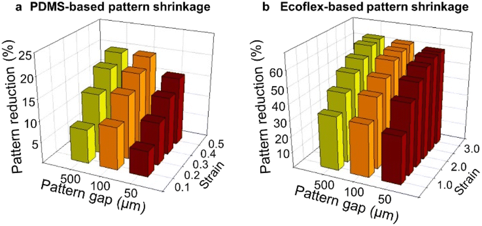 | ||
| Fig. 4 Quantitative comparison of the minimum achievable pattern dimensions using (a) PDMS and (b) Ecoflex as pre-stretched substrates. | ||
Microcontact printing
Fig. 5 presents the results of microcontact printing using the released Ecoflex stamp. The replicated pattern on the Ecoflex stamp, as shown in Fig. 5a, features a line pattern with an initial width and gap of approximately 4 μm, reduced from the original 10 μm line pattern according to the pre-strain of 3.0. We spin-coated the PR layer on top of this and defined the pattern on a prepared Si substrate by microcontact printing. Fig. 5b exhibits the optical images of the successfully defined PR pattern with a width of 4 μm. Additionally, to achieve sub-micrometer scale PR patterns, we used a stamp with a line pattern width of 800 nm, as shown in the optical micrograph in Fig. 5c. The line pattern of 800 nm in the stamp was obtained by shrinking a pattern originally obtained through I-line photolithography with a width of 2 μm according to the pre-strain of 3.0. Introducing the proposed fabrication process, we successfully achieved 800 nm line patterns, via microcontact printing, as shown in Fig. 5d. The quasi-opacity of Ecoflex in the visible range poses challenges for typically used top-view optical alignment. However, alternative alignment methods, particularly those utilizing the backside of the substrate, have been well established and widely adopted in photolithography processes.20 These processes commonly use wafer substrates, silicon with high transmission in the infrared range, and glass or quartz with high transmission in both the visible and infrared ranges. | ||
| Fig. 5 (a) Optical microscopy image of the replicated pattern on the Ecoflex stamp with the pre-strain of 3.0, showing the reduced line pattern to 4 μm from the original 10 μm dimensions. (b) Microcontact printing result of the replicated PR pattern. (c) Optical microscopy image of the stamp with the line pattern width reduced to 800 nm after the shrinkage from an initial 2 μm. (d) Successfully defined 800 nm PR line pattern using microcontact printing, demonstrating the effectiveness of the proposed shrink lithography process. | ||
Conclusions
In this study, the pattern gap was controlled by applying physical deformation of the stretchable Ecoflex substrate. We quantitatively controlled the magnitude of the external strain applied to Ecoflex, thereby determining the elongation ratio of the elastomer. As the elongation ratio increased, the reduction ratio of the pattern gaps also increased, which thereby achieved a 60% dimension reduction in the pattern. On the basis of the experimental results, we quantified the pattern deformation and confirmed a correlation between the applied strain and the dimensional reduction in the pattern. Consequently, by combining microcontact printing and shrinking lithography processes with conventional I-line photolithography, we successfully achieved an 800 nm periodic line array which is a 60% reduction in the dimension.Data availability
The datasets are available from the corresponding author on reasonable request.Author contributions
Conceptualization: J. S.; data analysis: E. J. and J. S.; methodology: E. J. and J. S.; resources: E. J. and J. S.; supervision: J. S.; visualization: E. J.; writing – original draft: E. J.; writing – review and editing: E. J. and J. S.Conflicts of interest
There are no conflicts to declare.Acknowledgements
This research was supported by the National R&D Program through the National Research Foundation of Korea (NRF) funded by the Ministry of Science and ICT (No. RS-2024-00348205).Notes and references
- S. Liu, J. Wang, J. Shao, D. Ouyang, W. Zhang, S. Liu, Y. Li and T. Zhai, Adv. Mater., 2022, 34, 2200734, DOI:10.1002/adma.202200734.
- J. Jung, K. K. Kim, Y. D. Suh, S. Hong, J. Yeo and S. H. Ko, Nanoscale Horiz., 2020, 5, 1036–1049, 10.1039/D0NH00241K.
- A. S. Gangnaik, Y. M. Georgiev and J. D. Holmes, Chem. Mater., 2017, 29, 1898–1917, DOI:10.1021/acs.chemmater.6b03483.
- S. Barcelo and Z. Li, Nano Convergence, 2016, 3, 21, DOI:10.1186/s40580-016-0081-y.
- S. Walia, C. M. Shah, P. Gutruf, H. Nili, D. R. Chowdhury, W. Withayachumnankul, M. Bhaskaran and S. Sriram, Appl. Phys. Rev., 2015, 2, 011303, DOI:10.1063/1.4913751.
- S. Surdo, S. Piazza, L. Ceseracciu, A. Diaspro and M. Duocastella, Appl. Surf. Sci., 2016, 374, 151–156, DOI:10.1016/j.apsusc.2015.10.142.
- C. Wu, H. Hsieh and Y. Lee, Micromachines, 2019, 10, 547, DOI:10.3390/mi10080547.
- S. Sayed and P. R. Selvaganapathy, Nanoscale Adv., 2020, 2, 5461–5467, 10.1039/D0NA00785D.
- W. Wang, Z. Zhao, H. Han, L. Li, D. Dai, Z. Zhang, J. Jin, S. Shao, L. Lu, W. Wang, C. Cheng, L. Liu and Q. Qu, Sci. Adv., 2022, 10, eadk4620, DOI:10.1126/sciadv.abn8338.
- X. Song, D. Fu, S. Shah and J. Reif, Adv. Mater. Technol., 2020, 5, 2000146, DOI:10.1002/admt.202000146.
- A. Lal Das, R. Mukherjee, V. Katiyer, M. Kulkarni, A. Ghatak and A. Sharma, Adv. Mater., 2007, 19, 1943–1946, DOI:10.1002/adma.200602681.
- S. Lin, E. K. Lee, N. Nguyen and M. Khine, Lab Chip, 2014, 14, 3475–3488, 10.1039/C4LC00528G.
- S. Sayed and P. R. Selvaganapathy, Microsyst. Nanoeng., 2022, 8, 20, DOI:10.1038/s41378-021-00338-y.
- W. M. Choi and O. O. Park, Microelectron. Eng., 2003, 3, 249–255, DOI:10.1016/S0167-9317(03)00436-2.
- S. Sim, E. Jo, Y. Kang, E. Chung and J. Kim, Small, 2021, 17, 2105334, DOI:10.1002/smll.202105334.
- D. Qi, K. Zhang, G. Tian, B. Jiang and Y. Huang, Adv. Mater., 2021, 33, 2003155, DOI:10.1002/adma.202003155.
- D. R. Darby, Z. Cai, C. R. Mason and J. T. Pham, J. Appl. Polym. Sci., 2022, 139, e52412, DOI:10.1002/app.52412.
- J. Vaicekauskaite, P. Mazurek, S. Vudayagiri and A. L. Skov, J. Mater. Chem. C, 2020, 8, 1273–1279, 10.1039/C9TC05072H.
- S. Park, K. Mondal, R. M. I. Treadway II, V. Kumar, S. Ma, J. D. Holbery and M. D. Dickey, ACS Appl. Mater. Interfaces, 2018, 10, 11261–11268, DOI:10.1021/acsami.7b18394.
- P. Pal, Y.-J. Kim and S. Chandra, Sens. Lett., 2006, 4, 1–10, DOI:10.1166/sl.2006.007.
Footnote |
| † Electronic supplementary information (ESI) available. See DOI: https://doi.org/10.1039/d4na00757c |
| This journal is © The Royal Society of Chemistry 2025 |