
 Open Access Article
 This Open Access Article is licensed under a
 Creative Commons Attribution 3.0 Unported Licence
Scratch-resistant sapphire nanostructures with anti-glare, anti-fogging, and anti-dust properties†
Kun-Chieh
Chien‡
,
Mehmet
Kepenekci‡
 ,
Andrew
Tunell
and
Chih-Hao
Chang
*
,
Andrew
Tunell
and
Chih-Hao
Chang
*
Walker Department of Mechanical Engineering, The University of Texas at Austin, Austin, Texas 78712, USA. E-mail: chichang@utexas.edu
First published on 11th February 2025
Abstract
Although there has been significant interest in the novel material properties of bio-inspired nanostructures, engineering them to become mechanically durable remains a significant challenge. This work demonstrates the fabrication of sapphire nanostructures with anti-glare, anti-fogging, anti-dust and scratch-resistant properties. The fabricated nanostructures demonstrated a period of 330 nm and an aspect ratio of 2.1, the highest reported for sapphire thus far. The nanostructured sapphire sample exhibited broadband and omnidirectional antireflection properties, with an enhanced transmission of up to 95.8% at a wavelength of 1360 nm. The sapphire nanostructures also exhibited enhanced wetting performance and could mitigate fogging from water condensation or repel water droplets. Furthermore, owing to their sharp features, the fabricated structures could prevent particulate adhesion and maintain a 98.7% dust-free surface area solely using gravity. Furthermore, nanoindentation and scratch tests indicated that the sapphire nanostructures have an indentation modulus and hardness of 182 GPa and 3.7 GPa, respectively, which are similar to those of bulk glass and scratch-resistant metals such as tungsten. These sapphire nanostructures can be fabricated using high-throughput nanomanufacturing techniques and can find applications in scratch-resistant optics for photonics, electronic displays, and protective windows.
New conceptsExisting windows with bio-inspired properties are generally made of silica-based glass and are not mechanically durable. This work demonstrates a novel transparent window made of sapphire nanostructures with anti-glare, anti-fogging, self-cleaning, and, most importantly, scratch-resistant properties. The new key concept is that by engineering the material composition and geometry of nanostructures, their material properties can be tailored in multiple physical domains. This work also provides the key insight that nanostructures can be as durable as smooth ceramic and scratch-resistant metal surfaces. |
I. Introduction
There has been significant interest in studying biological micro-/nanostructures that are found in nature, which have inspired engineered materials with novel physical properties. In optics, photonic nanostructures in butterflies (Morpho menelaus),1 green peacocks (Pavo muticus),2 and flower beetles (Torynorrhina flammea)3 have led to the fabrication of engineered materials with brilliant structural colors that can be dynamically tuned.4–6 In these photonic structures, light interference effects lead to structural coloration and a narrow reflectance band, which can be shifted to change the color appearance. Another example is the moth eye, where antireflection nanostructures with a tapered profile can minimize optical losses on the surface or interface of a material.7–15 These structures create a gradient-index medium, where the refractive index gradually changes to reduce Fresnel losses, and have been widely demonstrated in silicon, silica-based glass, and polymers.8–10,12,15,16 In addition to bioinspired hierarchical structures based on the moth eye, those based on brochosomes found in leafhoppers (Alnetoidia alneti) have demonstrated high antireflection properties.17,18Moreover, surface nanostructures can exhibit novel wetting properties after engineering geometric roughness and surface energy.12,16,19–26 The lotus leaf (Nelumbo nucifera) exhibits superhydrophobicity,19 where a water droplet in the Cassie–Baxter state has an extremely high water contact angle. Creating rough geometric features with lower surface energy enables the engineering of surfaces and devices with self-cleaning properties.12,16,22–26 Nanostructures with high surface energy can also improve fluid wetting, which has been observed in desert beetles (Stenocara sp.) for fog collection.20 In this regime, water droplets are in the Wenzel state, where the fluid fully wets the surface, and can lead to wicking effects and anti-fogging properties.12,21,23,25 In the design of bio-inspired nanostructures, one of the critical geometric parameters is the structure aspect ratio, which is defined by the ratio of the height (h) to the width (w). Recent work has shown that nanostructures with a high aspect ratio can lead to a broader wavelength band for antireflection and enhanced pressure robustness for maintaining superhydrophobicity.9 However, although a high aspect ratio can lead to improved physical properties, it also degrades the mechanical robustness of the structures.14 Therefore, one key challenge and an enabling factor for bio-inspired nanostructures is how to engineer structures with enhanced mechanical durability.
One potential method to improve the mechanical durability of nanostructured glass is the use of transparent ceramic materials, which have a higher bulk strength, stiffness, and hardness. One example is alumina-based sapphire, which has attractive optical, chemical, and mechanical properties.27–29 Sapphire can maintain an optical transmittance of greater than 80% in the range of 230 to 4400 nm, which is essential for optics operating in the broadband spectrum from ultraviolet (UV) to infrared (IR) region. Also, it has excellent mechanical properties, a Mohs hardness rating of 9, and Young's modulus of 350 GPa, and is scratch resistant. Furthermore, sapphire is temperature tolerant, chemically inert, and corrosion resistant, making it a compelling choice for extreme environments. Sapphire is widely used as a protective window for watches, electronics, and sensitive optical elements due to its high scratch resistance and optical transparency. One primary application of sapphire is windows and domes for defense and space applications,30 where it must withstand harsh launch conditions and maintain high infrared light transmission for optical signals.
Although bio-inspired nanostructures have been widely reported for silica-based glass, silicon, polymers, and other more traditional materials, they have been less explored for alumina-based glass. The challenge in creating high-density, high-aspect-ratio sapphire nanostructures can be attributed to the high mechanical hardness and chemical stability of sapphire, which makes traditional micromachining processes less effective. Microscale structures can be patterned on sapphire substrates using reactive ion etching (RIE),31–34 but they are too large to have effective antireflection and wetting properties. Recent work has demonstrated the successful patterning of sub-micrometer pillars or holes;35–38 however, these structures lack long-range spatial coherence and/or have an aspect ratio of less than 1. Furthermore, previous work required complex pattern transfer steps to enhance the etch selectivity of sapphire, resulting in a relatively high surface roughness and structure randomness, which can increase the optical scattering and reduce the optical clarity.
Herein, we demonstrate the fabrication of bio-inspired, multifunctional sapphire nanostructures with anti-glare, anti-fogging, self-cleaning, and scratch-resistant properties. Enabled by scalable nanolithography and advanced pattern transfer processes, the fabricated nanostructures were perfectly ordered with a period of 330 nm and low surface roughness. Furthermore, the fabricated structures possessed an aspect ratio of 2.1, the highest value reported in the literature for sapphire nanostructures to date. The fabricated sample was characterized using a spectrophotometer and demonstrated a broadband, omnidirectional antireflection effect. The sapphire nanostructures also exhibited anti-fogging and water-repelling properties by controlling the surface energy using surface functionalization. Furthermore, the fabricated structure demonstrated anti-dust properties by reducing the contact area with particulates. The indentation modulus and hardness of the sapphire nanostructures were characterized using nanoindentation and found to be similar to that of bulk glass and scratch-resistant metal. The demonstrated sapphire nanostructures have a unique combination of anti-glare, anti-dust scratch-resistance properties, and thus can be applied as protective windows, displays, and sensor surfaces for extreme environments.
II. Experimental approach
The nanostructures were patterned using interference lithography, and then transferred to a sapphire substrate using reactive ion etching. Sapphire has a low etching rate due to its chemical stability, and thus a thick polysilicon layer with a thickness of 1000 nm was deposited on the sapphire substrates for use as an etching mask. Subsequently, the samples were spin coated with a 100 nm-thick antireflection coating (Brewer Science, ARC i-con-7) and 200 nm-thick photoresist (Sumitomo, PFi-88A2). The photoresist was exposed using a Lloyd's mirror interference lithography (Kimmon HeCd laser, 325 nm wavelength) to pattern a 2D pillar array with a period of 330 nm. The photoresist pattern was transferred into the underlying ARC, polysilicon, and sapphire substrates using inductively coupled plasma reactive ion etching (ICP, Oxford 100) using O2, HBr, and BCl3/HBr gases, respectively. Notably, a low-RF power was used for the etching of the polysilicon layer with HBr RIE, which significantly increased the silicon to photoresist etch selectivity.39,40 This process resulted in a high aspect-ratio silicon mask from a low aspect-ratio resist structure and allows deep etching into the sapphire substrate. Subsequently, the structures was coated with a protective polymer film (Brewer Science, ProTEK B3-25), and the processing steps were repeated for the back side to create nanostructures on both sides of the substrate. The fabrication process is described in more detail in the Supporting Information A (ESI†).The fabricated sapphire nanostructures are depicted in the scanning electron microscopy (SEM) images shown in Fig. 1. Here, it can be observed that the sapphire nanostructures are periodic and have a tapered profile, as shown in Fig. 1(a). The structures were fabricated over an area of roughly 30 mm by 30 mm, and few defects could be observed. The structures were ordered in a square lattice with a period of 330 nm, as illustrated in the top-view SEM image shown in Fig. 1(b). Higher-magnification images are shown in Fig. 1(c) and (d) for the samples that were etched in BCl3/HBr RIE for 18 and 23 min, respectively. It can be observed that the tapered profile became increasingly sharp with longer etching times due to the shrinking of the polysilicon mask during RIE. The profile was controlled by the relative etching rates of the polysilicon vs. sapphire, and a more etch-resistant mask material could be used to create a slower taper. Over-etching of the sapphire structure once the mask is completely etched can lead to rounded taper, which can be mitigated by using end-point detection methods such as optical emission spectroscopy.40 The sample with a longer etch time possessed a feature width (w) of 240 nm and height (h) of 500 nm, which was used in all the characterization experiments. These dimensions resulted in an aspect ratio of h/w = 2.1, which is the highest value reported to date for sapphire nanostructures. In addition, the structure has relatively sharp tips with an estimated radius of 30 nm, which is important for reducing dust adhesion and will be discussed in the following sections. It is also important to note the structures have a low surface roughness, which is important for reducing optical scattering. The fabricated sample showed good uniformity over its entire area, with a shorter height of around 50 nm at the outer edge of the sample compared to the center. The boundary of the sample does not have any patterned nanostructures, which can be attributed to the formation of a non-uniform resist film due to edge effects during spin coating.
 | ||
| Fig. 1 SEM images of fabricated sapphire nanostructures. (a) Cross-section image of nanostructures with a 330 nm period and 400 nm height. (b) Top-view image of the structure with a square lattice. Higher magnification images of sapphire nanostructures with (c) 400 nm and (d) 500 nm heights. | ||
III. Results and discussion
A. Antireflection properties
The antireflection effects of the sapphire nanostructures were characterized using a UV-vis-NIR spectrophotometer (Agilent, Cary 5000), and the broadband transmittance in the wavelength range of 200 to 3000 nm for the planar, single-sided, and double-sided nanostructured sapphire substrates is shown in Fig. 2(a). The simulated transmittance was calculated using rigorous coupled-wave analysis (RCWA),41,42 as described in more detail in the Supporting Information B (ESI†), and agrees well with the data. It should be noted that sapphire has a relatively high optical refractive index of 1.7–1.8 in the visible to IR region, which can result in up to 15% reflection losses at normal incidence due to the high index mismatch. It can be observed that the transmittance of the single-sided and double-sided samples was higher than that of the planar sapphire for wavelengths longer than 550 nm. Overall, the average transmission from 550 to 3000 nm was 92.8% for the double-sided sample, 89.7% for the single-sided sample, and 86.7% for the planar sample. The maximum transmission for the double-sided sample was 95.8% at a wavelength of 1360 nm, in comparison to that of 91.1% and 85.9% for the single-sided and planar samples, respectively. This data agrees with the roughly 7.4% reflection loss for each of the planar sapphire surfaces at normal incident angle, which has an index of around ns = 1.75 at this wavelength. The absolute transmission enhancement of the nanostructures is around 9.9% for the double-sided sample and 5.2300% for the single-sided sample. The transmittance measurements indicate there are still reflection losses of around 4%, which can be attributed to the non-optimized profile near the valley of the structure. It can be observed that the duty-cycle of the structures abruptly ended at 0.85, which still resulted in an index mismatch to the substrate. Another source of loss is scattering losses due to fabrication defects and feature variations, which is compounded by double-sided patterning of the substrates. | ||
| Fig. 2 (a) Broadband transmittance of the planar, single-sided, and double-sided nanostructured sapphire samples. Transmission of (b) TE and TM and (c) non-polarized light versus the incident angle for the double-sided and planar sapphire samples at a wavelength of 1330 nm. (d) Visual demonstration of the anti-glare effects on color and black/white texts viewed through the double-sided nanostructured (left) and planar (right) sapphire samples. | ||
It can be observed that the antireflection effect gradual diminished at longer wavelengths, where the transmission of the double-sided nanostructured and planar samples at 3000 nm were 90.8% and 87.7%, respectively. This data shows an improvement of only 3.1%, which is much lower than the antireflection effect at shorter wavelengths. This effect can be attributed to the relatively short 500 nm height of the sapphire nanostructures, where the effective medium was not sufficiently tall for the longer operating wavelength. The maximum wavelength for effective antireflection can be approximated by,12λmax = 2hns![[thin space (1/6-em)]](https://www.rsc.org/images/entities/char_2009.gif) cosθi, where θi is the incident angle. The upper wavelength bound for the fabricated sapphire nanostructures was calculated to be λmax = 1750 nm, which agrees well with the transmittance data shown in Fig. 2(a). The antireflection effect at longer wavelengths can be improved by increasing the structure height, which requires deeper etches into the sapphire substrate. In the short wavelength regime, it was observed that the transmittance of both the single and double-sided nanostructured samples began to decrease for wavelengths shorter than 550 nm. This degradation can be attributed to diffraction, where the 1st-order diffractions were no longer evanescent but instead propagating orders trapped in the substrate as a waveguide mode. The lower wavelength bound to avoid diffraction effects can be approximated by,12λmin = Λ(ns + sinθi). In the case of the fabricated sapphire nanostructures, λmin = 570 nm, which agrees with the observed trend shown in Fig. 2. The λmin can be extended to the 300 nm range using structures with a shorter period in the range of 200 nm, as described further in Supporting Information B (ESI†).
cosθi, where θi is the incident angle. The upper wavelength bound for the fabricated sapphire nanostructures was calculated to be λmax = 1750 nm, which agrees well with the transmittance data shown in Fig. 2(a). The antireflection effect at longer wavelengths can be improved by increasing the structure height, which requires deeper etches into the sapphire substrate. In the short wavelength regime, it was observed that the transmittance of both the single and double-sided nanostructured samples began to decrease for wavelengths shorter than 550 nm. This degradation can be attributed to diffraction, where the 1st-order diffractions were no longer evanescent but instead propagating orders trapped in the substrate as a waveguide mode. The lower wavelength bound to avoid diffraction effects can be approximated by,12λmin = Λ(ns + sinθi). In the case of the fabricated sapphire nanostructures, λmin = 570 nm, which agrees with the observed trend shown in Fig. 2. The λmin can be extended to the 300 nm range using structures with a shorter period in the range of 200 nm, as described further in Supporting Information B (ESI†).
In addition to broadband behavior, the specular transmission as a function of incident angle was also investigated to demonstrate the omnidirectional behavior of the samples. The transmission of TE and TM-polarized light for the planar and double-sided nanostructured sapphire samples was measured versus incident angle in the range of 0° to 80° at 1330 nm, as shown in Fig. 2(b). It can be observed that both angle-dependent data agree well with the RCWA model. In the case of TE-polarized light, the transmission of the nanostructured sample was enhanced across all incident angles. Notably, at a high incident angle of 60°, the transmission was over 80%, which is a significant enhancement compared to the planar sample, which decreased to 54.2%. In the case of TM-polarized light, the double-sided nanostructured sample maintained transmission over 90% for incident angles from 0° to 60°, and no pronounced Brewster peak could be observed due to the suppression of the discrete index mismatch at the interface. Alternatively, the transmission of the planar sapphire had a peak at 60.3°, which agrees with the calculated Brewster angle at the air/sapphire interface.
The non-polarized transmission is the average of the TE and TM-polarized measurements, as shown in Fig. 2(c). Here, it can be observed that the sapphire sample with the nanostructures showed enhanced transmission at all incident angles. Notably, the non-polarized light transmission of the nanostructured sample could be maintained at around 90% for incident angles up to 60°. On the contrary, the transmission of the planar sample dropped to 76.4%. In addition, the planar sample exhibited a more pronounced decrease in transmission at high oblique incident angles, with a marked reduction to 38.4% at 80°. In contrast, the nanostructured sample could maintain 55.0% under the same conditions. Therefore, the antireflection effect was more pronounced at higher incident angle, where the absolute transmission enhancement increased from 12.4% at normal incident to 16.6% at 80°. The data confirms that the sapphire nanostructures have omnidirectional antireflection effects and can enhance the light transmission for all polarization states and wide incident lights.
The anti-glare effects in the fabricated sapphire samples could be visually observed, as illustrated in Fig. 2(d). Here, two camera images of the double-sided nanostructured and planar sapphire samples are placed over printed color and black/white texts on paper and illuminated with ambient white light. In both images the glare of the nanostructured sample can be observed to be significantly lower, resulting in high visibility of the underlying text through the nanostructured sample. In contrast, the planar sample has high glare, and the underlying text cannot be visually identified. It should be noted that a slight purple tint can be observed on the nanostructured sample, which can be attributed to the reduction in the antireflection effects at shorter wavelengths. This effect can be mitigated by further reducing the period of the sapphire nanostructures to 200 nm, enabling the operating range to be shifted to a shorter wavelength, as described in the previous section. It is important to note that glare can be observed at the boundary of the sample, where there are no patterned nanostructures due to edge effects during processing.
B. Anti-fogging properties
In addition to antireflection effects, the untreated sapphire nanostructures also exhibited anti-fogging effects. This effect can be attributed to the high surface energy of sapphire and its high aspect ratio, resulting in a superhydrophilic surface in the Wenzel state with a measured contact angle of close to 0°.43,44 This structure is also in the wicking state, and any water droplet on its surface is wicked into its structure. As a result, any water condensation forms a thin water film rather than microdroplets with random sizes, which reduces light scattering and mitigates the fogging effect. The anti-fogging effect of the bio-inspired nanostructured sapphire sample is illustrated in Fig. 3. Here, a cup of hot water with steam was placed under the double-sided nanostructured and planar sapphire samples for 10 s and the water condensation event was recorded (see Video S1, ESI†). The extracted frame before water condensation is shown in Fig. 3(a), where both the nanostructured and planar samples have high clarity and the logo on the display screen behind the samples are visible. The frame after introducing the steam for 2 s is shown in Fig. 3(b), where the water condensation on the planar sample results in significant fogging and the logos are obscured. Alternatively, very little fogging can be observed on the nanostructured sample, and the logos are still clear with high visibility. It is important to note that fogging can be observed at the edge of the nanostructured samples, where there are patterns due to the edge effects during processing. | ||
| Fig. 3 Images of the double-sided nanostructured (left) and planar (right) sapphire samples (a) before and (b) after water condensation. Measured broadband transmission (c) before and (d) after water condensation on double-sided (orange), single-sided (red), and planar (blue) sapphire surfaces. Time evolution of optical transmission at (e) 632 nm and (f) 980 nm due to fogging and defogging on double-sided (orange), single-sided (red), and planar sapphire (blue) substrates. | ||
To examine the transient effect of the anti-fogging behavior, the specular transmission of the double-sided, single-sided nanostructured, and planar sapphire samples was measured using a broadband spectrometer (Ocean Insight HR4Pro). The measured transmittance in the range of 300 to 1000 nm before and after water condensation is shown in Fig. 3(c) and (d), respectively. It can be observed that the transmission of the planar samples dropped to below 10% across the entire wavelength range after fog formation. In contrast, the double-sided sample maintained a transmission of above 80% for wavelengths longer than 540 nm, demonstrating a strong anti-fogging effect. The slight reduction in transmission can be attributed to the thin water film formed on the nanostructures, which can result in reflection losses due to index mismatch.
Furthermore, two commonly used laser wavelengths in the visible (632 nm) and near-IR range (980 nm) were selected to represent the time evolution of the transmission during the water condensation and evaporation processes, as shown in Fig. 3(e) and (f), respectively. During the 1-s water condensation period, the transmission of the planar sample significantly dropped to below 10% at both wavelengths, while the single-sided and double-sided samples maintained a transmission above 70% and 80%, respectively. Moreover, it took about 6 s for the water to evaporate from the planar sample and fully recover its optical transmission. In contrast, the recovery time for the double-sided nanostructure samples improved to around 1 s. The faster recovery can be attributed to the thin water film on the nanostructure having a higher water-sapphire interfacial area, allowing the water to evaporate faster. Although there was a slight drop in transmission for the double-sided sample during the water condensation process, the difference was difficult to observe with the naked eye given that the transmission remained above 80%.
C. Self-cleaning properties
In addition to an anti-fogging effect, the sapphire nanostructures also exhibited a self-cleaning effect by tuning their surface chemistry. Inspired by the lotus leaf, one way to achieve a self-cleaning surface is to induce superhydrophobicity in the Cassie–Baxter state, where the water droplet does not fully wet the structures.12,16,45–47 In this state the water droplet has low adhesion to the structure can remove any particle contamination through surface tension. High aspect-ratio structures also play a key role in maintaining pressure robustness, where a high impact velocity or pressure can induce a Cassie–Baxter to Wenzel state transition.12,16,43,48 To reduce the surface energy, the double-sided nanostructured and planar samples were treated with oxygen plasma etching to promote hydroxylation on their surface and coated with trichloro(octyl)silane through vapor phase deposition. After treatment, the static water contact angle (θ) of the planar sapphire surface increased to θ = 98.9° due the reduction in surface energy. The high structure aspect ratio induced the Cassie–Baxter state, where the apparent contact angle (θ*) for the nanostructured sapphire surface increased to θ* = 144.2°. The contact angle hysteresis (CAH) and roll-off angle of the sapphire nanostructures was measured to be about 12.2°, as described further in Supporting Information C (ESI†). The wetting characterization indicates that the fabricated sapphire nanotextured surface is close to being superhydrophobic, which is typically defined as θ* > 150° and CAH < 10°. The slightly lower contact angles can be attributed to fabrication defects in the sapphire nanostructures, which increase surface friction during droplet motion.The dynamic wetting behavior of water droplets at low and high velocities on the nanostructured sapphire sample was captured by a high-speed camera (Phantom Miro C321), as illustrated in Fig. 4. At low velocity, the droplet can be observed to completely roll off the nanostructure sapphire sample at an incline angle of 20°, as shown in Fig. 4(a). Here, the water was dispensed by a pipette close to the sample, and no droplet pinning can be observed. To demonstrate the high pressure robustness, the wetting response at higher droplet velocity was examined, as shown in Fig. 4(b). Here, the water was dropped at elevated height and had an impact velocity of 1 m s−1 on the sapphire nanostructures, which was inclined at 50°. It can be observed that the droplet completely rebound from the impact, indicating that the Cassie–Baxter state was maintained. At higher impact velocity, the droplet can be observed to be partially pinned after impact, indicating the that the droplet transitioned to the Wenzel state. The maximum velocity can be improved by further increasing the aspect ratio of the sapphire nanostructures. The videos of low and high velocity impact are available as Videos S2 and S3 (ESI†), respectively.
 | ||
| Fig. 4 Extracted frames from high-speed camera of water droplets falling on the sapphire nanostructures. (a) At low velocity, water droplet falls on the nanostructure sample at a 20° incline angle and rolls off. (b) At a velocity of 1 m s−1, the droplet impacts the nanostructure sample at a 50° oblique angle and completely rebounds. | ||
In conjunction with repelling water, the surface nanostructures can also facilitate anti-dust property by reducing particle adhesion to the surface. This effect leads to the well-documented self-cleaning effect, where water droplets are used to remove particle contamination on the surface through surface tension. However, recent work has demonstrated that if the particle adhesion force can be mitigated, the cohesion of particles to form larger aggregates can be an effective mechanism for dust removal.26 This effect is important for dust mitigation in space or applications where water is not readily available. Thus, to examine this dry self-cleaning effect, the adhesion of a particle with a surface nanostructure can be approximated by the Johnson–Kendall–Roberts (JKR) model,26,49–51 as follows:

The anti-dust property of the fabricated sapphire nanostructures were tested by using lunar dust simulant (Exolith Labs LMS-1), which consisted primarily of oxides and had a broad size range with an average value of around 50 μm.52 In this experiment, a layer of dust was applied onto the double-sided nanostructured and planar sapphire samples, which were then tilted vertically to allow the dust to be removed via gravity (see Video S4, ESI†), as shown in Fig. 5. Confocal microscopy (Keyence VK-X1100) was utilized to generate a topographic map of the contaminated surface, allowing any raised point to be identified as residual dust. The optical microscope images of the planar and double-sided nanostructured samples are shown in Fig. 5(a) and (b), respectively. Here, it can be observed that the dust particles cover a significant portion of the planar sapphire sample, while they are mostly removed from the nanostructured samples. The percentage area coverage of dust was used to compare the relative dust mitigating performance of these two samples. Based on 30 confocal images, the average dust coverage for each sample was determined to be 31.8% ± 2.7% and 1.3% ± 0.8% for the planar and nanostructured samples, respectively. This data shows a 95.9% reduction in residual dust coverage and is better than existing anti-dust polymer and metal surfaces.26,53 The calculation of the dust coverage and raw confocal images is described in more detail in Supporting Information D (ESI†).
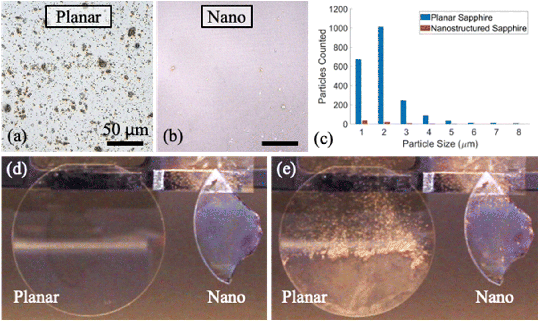 | ||
| Fig. 5 Demonstration of the anti-dust effect by the sapphire nanostructure. Top-view optical microscopic images of (a) planar and (b) nanostructured samples after dust application; the percentage area covered by dust is 31.8% and 1.3%, respectively. (c) Histogram of residual particles on both samples using confocal microscopy. Camera images of the planar and nanostructured samples (d) before and (e) after dust application and removal via gravity. | ||
The histograms of the residual particle on the planar and nanostructured sapphire samples are shown in Fig. 5(c), where particles smaller than 8 μm are examined given that most large particles were removed via gravity for both samples. Here, it can be observed that a significant number of particles remained on the planar sample, with 671 and 1012 particles counted with diameters of less than 1 and 2 μm, respectively. Alternatively, the nanostructured samples have only 36 and 21 for the corresponding two sizes, demonstrating a 20 and 50-fold reduction in residual particles, respectively. The calculation of the histogram is described in more detail in Supporting Information D (ESI†). The anti-dust property of the sapphire nanostructures can be visually observed. The extracted frames of the planar and double-sided nanostructures samples before and after the application of dust are shown in Fig. 5(d) and (e), respectively. Here, it can be observed that a layer of dust remained on the planar but mostly removed from the nanostructured sample. It is interesting to note there are small patches of residual dust on the edges of the nanostructured sample, which are regions on the substrate with no structures.
D. Scratch-resistant properties
In previous sections, the multifunctional sapphire nanostructures demonstrated effective anti-glare, anti-fogging, and self-cleaning properties. However, the durability of the nanostructures is a critical parameter that can limit their broad implementation. This is especially important given that sapphire is often used in harsh environments involving high temperatures and abrasion. Thus, the mechanical properties of the sapphire nanostructures were characterized using nanoindentation (Bruker, Hysitron TI 950 Triboindenter). A conospherical indenter with a cone angle of 90° and tip radius of 10 μm was used to ensure that multiple nanostructures were in contact. The mechanical response was measured using both quasi-static and cyclic partial loading-unloading indentation test methods with load control, as shown in Fig. 6. The indentation modulus and hardness values were extracted from the force vs. displacement curves using the Oliver-Pharr method.54 The indentation depth was limited to around 10–20% of the structure height to mitigate the substrate effect. | ||
| Fig. 6 Nanoindentation and scratch testing of sapphire nanostructures. (a) Load-displacement plot of a quasi-static nanoindentation test. Inset SEM image shows the test region after indentation. (b) Measured hardness and (c) indentation modulus vs. depth for quasi-static and cyclic tests. (d) Picture of the specimen after the pencil hardness testing showing the scratch mark. SEM image of sapphire nanostructures in the pencil test region (e) before and (f) after cleaning. | ||
A representative quasi-static indentation curve is shown in Fig. 6(a). Here, the indentation depth was around 64 nm at the maximum load of 3700 μN, and the inset SEM image shows the sapphire nanostructures after testing. It can be observed that the structures are mostly intact without any observable damage. The measured indentation modulus and hardness versus depth are shown in Fig. 6(b) and (c), respectively. Both quasi-static and cyclic tests were plotted and provide similar results. It can be observed that both the modulus and hardness increased with the indentation depth, which can be attributed to the tapered profile with an increasing solid volume fraction at the valley of the nanostructures. At the highest depth of 90 nm, the measured modulus and hardness were 182 GPa and 3.7 GPa, respectively. In comparison, the indentation modulus and hardness of the bulk sapphire were 440 GPa and 30 GPa, respectively.54,55 Here, it can be observed that the modulus has relatively low degradation given the ordered geometry of the nanostructure, which led to improved modulus vs. density scaling. The higher degradation in the hardness can be attributed to the relative ease of deforming the nanostructures versus a planar surface. It is important to note that the sapphire nanostructures have higher stiffness and similar hardness compared with the commonly used bulk glass, which for soda lime glass are 70 and 6 GPa, respectively.54 The nanostructured sapphire surface is also as hard as tungsten, a scratch-resistant metal with hardness of around 4 GPa.54 The detailed calculations and additional quasi-static and cyclic nanoindentation tests are shown in Supporting Information E (ESI†).
The scratch-resistant property of the multifunctional sapphire nanostructures was tested using pencil hardness testing (Elcometer 501) by following the standard ASTM D3363 testing protocol. In this experiment the sample was scratched with a control load of 7.5 N at an angle of 45° with pencil probes of various hardness. A camera image of the sample after the scratch testing with a 2B pencil is shown in Fig. 6(d). Here, a clear pencil mark can be observed, indicating that the graphite pencil has lower hardness and is scratched. The SEM image of the sapphire nanostructures after pencil testing is shown in Fig. 6(e), which shows the graphite debris in between the structures. It can be noted that the nanostructures are undamaged. The graphite marks were removed using RCA and piranha solution, and the cleaned structures are shown in Fig. 6(f). Here it can be observed that the structures are undamaged, indicating the scratch resistance of the sapphire nanostructures. However, some of the structures were damaged at increasing pencil hardness, which can be attributed to the high load of the test. These results indicate that the sapphire nanostructures are scratch resistant with similar hardness to bulk glass and scratch-resistant metals such as tungsten.
E. Discussion and future work
The fabricated sapphire nanostructures demonstrated anti-glare, anti-fogging, self-cleaning, and most importantly scratch-resistant behavior. It is expected that these physical properties can be further improved by increasing the aspect ratio of the structures, which is currently around 2. By reducing the structure period and increasing the structure height, the antireflection is expected to be more effective in the short and long wavelength regimes, respectively. The apparent contact angle can also be increased and the CAH reduced by having a higher aspect ratio, thereby reducing the liquid contact area at the tip of the structures. The increase in surface roughness can also enhance the pressure robustness and maintain superhydrophobicity for droplets at a higher velocity. In addition, structures with small features can also reduce the contact area and adhesion force of particles, which can lead to better anti-dust properties. Deeper etching into sapphire can be achieved by further optimizing the RIE parameters and using a thicker etch mask. However, it is important to note that although a higher structure aspect ratio can improve the optical, wetting, and self-cleaning behavior, it can potentially degrade the mechanical properties. This effect can be attributed to the scaling of the mechanical behavior in porous, cellular materials, which generally degrades at a reduced volume fraction.56,57 The degradation in stiffness is expected to be low in the sapphire nanostructures given that they are ordered and periodic, which can have enhanced stiffness vs. density scaling. Alternatively, the degradation in hardness is expected to be more significant given that high-aspect-ratio structures are more prone to mechanical damage.In addition to the aspect ratio, the geometric profile of the sapphire nanostructures can also be designed to improve their optical, self-cleaning, and mechanical behavior. A more gradual taper, where the duty cycle is continuously varied from 0 to 1, can create an improved gradient-index medium and further enhance the anti-glare effect. Creating nanostructure tips with lower curvature radius can also reduce the contact area with particle contaminants, which can lead to improved anti-dust properties. However, these sharp features are expected to be more prone to mechanical damage and wear, which can reduce the hardness of the nanostructures. Future work will focus on investigating the competing effects of optical, wetting, adhesion, and mechanical properties in relation to the structure aspect ratio and profile geometry.
In addition to demonstrating mechanical robustness, another key limitation in the broad applications of engineered surfaces is manufacturing challenges. In this work, the sapphire nanostructures were patterned over an area of 30 mm by 30 mm for demonstration of their material properties, but the developed process is scalable for larger areas. The nanostructures were patterned using interference lithography, which is a parallel patterning technique that has been adopted for meter-size substrates.58 Furthermore, given that only a thin polymer structure is need for the pattern transfer step, other high-throughput processes such as nanoimprint lithography can also be used.59–61 By being compatible with existing nanomanufacturing processes, the scratch-resistant multifunctional sapphire nanostructures can be potentially adopted in a wide array of industries such as electronics, optics, and aerospace.
IV. Summary
This work demonstrated the fabrication of sapphire nanostructures with anti-glare, anti-fogging, and self-cleaning properties, which are also mechanically durable and scratch resistant. Through the large-area pattern transfer of nanostructures into a hard transparent ceramic substrate, the fabricated sapphire nanostructures exhibited an aspect ratio of 2.1, the highest reported to date for sapphire. The double-sided sapphire nanostructure sample exhibited enhanced specular transmission in the wavelength range of 550 to 3000 nm and incident angles of 0° to 80°, with a peak transmission of 95.8% at a wavelength of 1360 nm. The sapphire nanostructures also exhibited strong anti-fogging properties and maintained over 80% transmission during water condensation. Furthermore, by changing their surface chemistry, the sapphire nanostructures demonstrated superhydrophobicity and effective anti-dust properties, where 98.7% of their surface was free from dust when the substrate was tilted via gravity. Using nanoindentation, the measured modulus and hardness of the sapphire nanostructures were 182 GPa and 3.7 GPa, respectively, which are similar to that of bulk glass and scratch-resistant metals such as tungsten. These results indicate that the anti-glare, anti-fogging, and anti-dust sapphire nanostructures are also scratch resistant and can find application in protective windows, infrared optics, and sensor surfaces that are used in extreme environments.V. Methods
A. Nanostructure fabrication
The sapphire nanostructures were patterned using interference lithography and transferred via multilayer reactive ion etching. Initially, a 1 μm-thick polysilicon layer was deposited as the etch mask on a 100 mm sapphire substrate (single crystal with c-plane cut) using low-pressure chemical vapor deposition (LPCVD). The samples were spin coated with a 100 nm-thick antireflection coating (Brewer Science, ARC i-con-7) to reduce the back reflection during lithography, and then coated with a 200 nm-thick photoresist (Sumitomo, PFi-88A2). A Lloyd's mirror interference lithography setup with an HeCd laser (325 nm wavelength) was used to pattern a 2D pillar array in a square lattice with period of 330 nm in the samples. The photoresist pattern was transferred into the underlying ARC, polysilicon, and sapphire substrates using inductively coupled plasma reactive ion etching (ICP, Oxford 100) using O2, HBr, and BCl3/HBr gases, respectively. Then, the structures were coated with a protective polymer film (Brewer Science, ProTEK B3-25), and the processing steps were repeated for the back side to create nanostructures on both sides of the substrate.B. Surface treatment
The nanostructured and planar sapphire substrates were cleaned with isopropanol and treated with oxygen plasma etching (Harrick Plasma, PDC-32G) for 10 s at 500 mTorr pressure and 6.8 W power to activate the surface hydroxyl groups. Then, the sample was placed inside a vacuum desiccator with a Petri dish containing 100 μL of trichloro(octyl)silane (97%, Sigma Aldrich). After the pressure in the desiccator was reduced to around 1 Torr, the samples were treated for at least 6 h to form a monolayer of covalent silane bonds via vapor phase deposition.Author contributions
C.-H. C and K.-C. C. conceived of the presented idea. K.-C. C. fabricated the experimental samples and characterized the optical and wetting properties. M. K. performed the mechanical characterization and formulated the deformation mechanisms, as well as the optical modeling of the samples. A. T. performed the dust adhesion experiments and helped organize the data. All authors took part in the writing of the manuscript. C.-H. C. supervised the project.Data availability
All data are available in the main text or the ESI.†Conflicts of interest
The authors have no conflicts to disclose.Acknowledgements
This work was performed at UT Austin Texas Materials Institute (TMI), the Nanomanufacturing System for mobile Computing and Energy Technologies (NASCENT), and Texas Nanofabrication Facilities, which is supported by the National Science Foundation (NSF) as part of the National Nanotechnology Coordinated Infrastructure (NNCI) grant NNCI-2025227. This work is funded by Army Research Office (ARO) under grant W911NF-22-1-0124, and National Aeronautics and Space Administration (NASA) under grants 80NSSC22CA124 and 80NSSC25K7279, and the National Science Foundation (NSF) under grant TI-2314268.References
- P. Vukusic, J. R. Sambles, C. R. Lawrence and R. J. Wootton, Quantified interference and diffraction in single Morpho butterfly scales, Proc. R. Soc. London, Ser. B, 1999, 266, 1403–1411 Search PubMed.
- J. Zi, et al., Coloration strategies in peacock feathers, Proc. Natl. Acad. Sci., 2003, 100, 12576–12578 CrossRef CAS PubMed.
- Z. Jia, et al., Microstructural design for mechanical–optical multifunctionality in the exoskeleton of the flower beetle Torynorrhina flammea, Proc. Natl. Acad. Sci., 2021, 118, e2101017118 Search PubMed.
- G. Isapour and M. Lattuada, Bioinspired stimuli-responsive color-changing systems, Adv. Mater., 2018, 30, 1707069 Search PubMed.
- Z. Luo, E. E. Evans and C.-H. Chang, Magnetically actuated dynamic iridescence inspired by the neon tetra, ACS Nano, 2019, 13, 4657–4666 CrossRef CAS PubMed.
- Y. Liu, et al., Structural color three-dimensional printing by shrinking photonic crystals, Nat. Commun., 2019, 10, 4340 CrossRef PubMed.
- P. B. Clapham and M. C. Hutley, Reduction of Lens Reflexion by the “Moth Eye” Principle, Nature, 1973, 244, 281–282 CrossRef.
- P. Lalanne and G. M. Morris, Antireflection behavior of silicon subwavelength periodic structures for visible light, Nanotechnology, 1997, 8, 53–56 CrossRef CAS.
- Y. Kanamori, M. Sasaki and K. Hane, Broadband antireflection gratings fabricated upon silicon substrates, Opt. Lett., 1999, 24, 1422–1424 Search PubMed.
- P. Vukusic and J. R. Sambles, Photonic structures in biology, Nature, 2003, 424, 852–855 Search PubMed.
- Y.-F. Huang, et al., Improved broadband and quasi-omnidirectional anti-reflection properties with biomimetic silicon nanostructures, Nat. Nanotechnol., 2007, 2, 770–774 Search PubMed.
- K.-C. Park, et al., Nanotextured Silica Surfaces with Robust Superhydrophobicity and Omnidirectional Broadband Supertransmissivity, ACS Nano, 2012, 6, 3789–3799 Search PubMed.
- Q. Yang, X. A. Zhang, A. Bagal, W. Guo and C.-H. Chang, Antireflection effects at nanostructured material interfaces and the suppression of thin-film interference, Nanotechnology, 2013, 24, 235202 CrossRef PubMed.
- J.-G. Kim, et al., Multifunctional Inverted Nanocone Arrays for Non-Wetting, Self-Cleaning Transparent Surface with High Mechanical Robustness, Small, 2014, 10, 2487–2494 CrossRef CAS PubMed.
- Y.-A. Chen, S. V. Naidu, Z. Luo and C.-H. Chang, Enhancing optical transmission of multilayer composites using interfacial nanostructures, J. Appl. Phys., 2019, 126, 063101 Search PubMed.
- A. Lafuma and D. Quéré, Superhydrophobic states, Nat. Mater., 2003, 2, 457–460 Search PubMed.
- S. Yang, et al., Ultra-antireflective synthetic brochosomes, Nat. Commun., 2017, 8, 1285 CrossRef PubMed.
- L. Wang, Z. Li, S. Shen and T.-S. Wong, Geometric design of antireflective leafhopper brochosomes, Proc. Natl. Acad. Sci., 2024, 121, e2312700121 Search PubMed.
- W. Barthlott and C. Neinhuis, Purity of the sacred lotus, or escape from contamination in biological surfaces, Planta, 1997, 202, 1–8 CrossRef CAS.
- A. R. Parker and C. R. Lawrence, Water capture by a desert beetle, Nature, 2001, 414, 33–34 Search PubMed.
- F. Ç. Cebeci, Z. Wu, L. Zhai, R. E. Cohen and M. F. Rubner, Nanoporosity-driven superhydrophilicity: a means to create multifunctional antifogging coatings, Langmuir, 2006, 22, 2856–2862 Search PubMed.
- J. Zhu, C.-M. Hsu, Z. Yu, S. Fan and Y. Cui, Nanodome solar cells with efficient light management and self-cleaning, Nano Lett., 2010, 10, 1979–1984 CrossRef CAS PubMed.
- S. Haghanifar, et al., Creating glasswing butterfly-inspired durable antifogging superomniphobic supertransmissive, superclear nanostructured glass through Bayesian learning and optimization, Mater. Horiz., 2019, 6, 1632–1642 RSC.
- A. Pan, H. Lu and L.-Z. Zhang, Experimental investigation of dust deposition reduction on solar cell covering glass by different self-cleaning coatings, Energy, 2019, 181, 645–653 CrossRef CAS.
- S. Haghanifar, A. J. Galante and P. W. Leu, Challenges and prospects of bio-inspired and multifunctional transparent substrates and barrier layers for optoelectronics, ACS Nano, 2020, 14, 16241–16265 CrossRef CAS PubMed.
- S. S. Lee, et al., Engineering Large-Area Antidust Surfaces by Harnessing Interparticle Forces, ACS Appl. Mater. Interfaces, 2023, 15, 13678–13688 Search PubMed.
- B. S. Patel and Z. H. Zaidi, The suitability of sapphire for laser windows, Meas. Sci. Technol., 1999, 10, 146 CrossRef CAS.
- V. N. Kurlov, Sapphire: Properties, Growth, and Applications. Encyclopedia of Materials: Science and Technology, 2001, pp. 8259–8264 DOI:10.1016/B0-08-043152-6/01478-9.
- E. R. Dobrovinskaya, L. A. Lytvynov and V. Pishchik, Sapphire: Material, Manufacturing, Applications, Springer Science & Business Media, 2009 Search PubMed.
- L. M. Goldman, R. Twedt, S. Balasubramanian and S. Sastri, ALON optical ceramic transparencies for window, dome, and transparent armor applications, in Window and Dome Technologies and Materials XII, SPIE, 2011, vol. 8016, pp. 64–77 Search PubMed.
- C. H. Jeong, et al., Sapphire etching with BCl3/HBr/Ar plasma, Surf. Coat. Technol., 2003, 171, 280–284 CrossRef CAS.
- Y. P. Hsu, et al., ICP etching of sapphire substrates, Opt. Mater., 2005, 27, 1171–1174 CrossRef CAS.
- W.-K. Wang, et al., Efficiency improvement of near-ultraviolet InGaN LEDs using patterned sapphire substrates, IEEE J. Quantum Electron., 2005, 41, 1403–1409 CAS.
- J. W. Leem and J. S. Yu, Wafer-scale highly-transparent and superhydrophilic sapphires for high-performance optics, Opt. Express, 2012, 20, 26160–26166 CrossRef CAS PubMed.
- H. Park, K.-J. Byeon, J.-J. Jang, O. Nam and H. Lee, Enhancement of photo- and electro-luminescence of GaN-based LED structure grown on a nanometer-scaled patterned sapphire substrate, Microelectron. Eng., 2011, 88, 3207–3213 CrossRef CAS.
- H. Chen, Q. Zhang and S. Y. Chou, Patterning of light-extraction nanostructures on sapphire substrates using nanoimprint and ICP etching with different masking materials, Nanotechnology, 2015, 26, 085302 CrossRef CAS PubMed.
- Y.-A. Chen, K.-C. Chien, I.-T. Chen and C.-H. Chang, Sapphire nanophotonics: Fabrication challenges and optical properties, Micro Nano Eng., 2022, 14, 100115 CrossRef CAS.
- S. Tzadka, et al., A Novel Approach for Colloidal Lithography: From Dry Particle Assembly to High-Throughput Nanofabrication, ACS Appl. Mater. Interfaces, 2024, 16, 17846–17856 Search PubMed.
- K.-C. Chien and C.-H. Chang, Controlling the etch selectivity of silicon using low-RF power HBr reactive ion etching, J. Vac. Sci. Technol., B, 2022, 40, 062802 Search PubMed.
- K.-C. Chien, N. Graff, D. Djurdjanovic and C.-H. Chang, In situ monitoring of sapphire nanostructure etching using optical emission spectroscopy, J. Vac. Sci. Technol., B, 2023, 41, 062807 Search PubMed.
- M. G. Moharam, D. A. Pommet, E. B. Grann and T. K. Gaylord, Stable implementation of the rigorous coupled-wave analysis for surface-relief gratings: enhanced transmittance matrix approach, J. Opt. Soc. Am. A, 1995, 12, 1077–1086 CrossRef.
- M. G. Moharam, E. B. Grann, D. A. Pommet and T. K. Gaylord, Formulation for stable and efficient implementation of the rigorous coupled-wave analysis of binary gratings, J. Opt. Soc. Am. A, 1995, 12, 1068–1076 CrossRef.
- R. N. Wenzel, Resistance of solid surfaces to wetting by water, Ind. Eng. Chem., 1936, 28, 988–994 CrossRef CAS.
- J. Bico, C. Tordeux and D. Quéré, Rough wetting, EPL, 2001, 55, 214 CrossRef CAS.
- M. Nosonovsky and B. Bhushan, Roughness optimization for biomimetic superhydrophobic surfaces, Microsyst. Technol., 2005, 11, 535–549 Search PubMed.
- C.-H. Choi and C.-J. Kim, Large Slip of Aqueous Liquid Flow over a Nanoengineered Superhydrophobic Surface, Phys. Rev. Lett., 2006, 96, 066001 CrossRef PubMed.
- N. Cherupurakal, M. Mozumder, A. Mourad and S. Lalwani, Recent advances in superhydrophobic polymers for antireflective self-cleaning solar panels, Renewable Sustainable Energy Rev., 2021, 151, 111538 CrossRef CAS.
- A. B. D. Cassie and S. Baxter, Wettability of porous surfaces, Trans. Faraday Soc., 1944, 40, 546–551 RSC.
- K. L. Johnson, K. Kendall, A. D. Roberts and D. Tabor, Surface energy and the contact of elastic solids, Proc. R. Soc. London, Ser. A, 1971, 324, 301–313 CAS.
- B. V. Derjaguin, V. M. Muller and Yu. P. Toporov, Effect of contact deformations on the adhesion of particles, J. Colloid Interface Sci., 1975, 53, 314–326 Search PubMed.
- P. Prokopovich and S. Perni, Comparison of JKR- and DMT-based multi-asperity adhesion model: Theory and experiment, Colloids Surf., A, 2011, 383, 95–101 CrossRef CAS.
- Lunar Mare (LMS-1) High-Fidelity Moon Dust Simulant. Space Resource Technologies https://spaceresourcetech.com/products/lms-1-lunar-mare-simulant Search PubMed.
- X. Wang, et al., Rapid Fabrication of Antilunar Dust Aluminum Surface by Nanosecond Laser Etching, ACS Appl. Mater. Interfaces, 2024, 16, 45678–45686 CrossRef CAS PubMed.
- W. C. Oliver and G. M. Pharr, An improved technique for determining hardness and elastic modulus using load and displacement sensing indentation experiments, J. Mater. Res., 1992, 7, 1564–1583 CrossRef CAS.
- W. G. Mao, Y. G. Shen and C. Lu, Nanoscale elastic–plastic deformation and stress distributions of the C plane of sapphire single crystal during nanoindentation, J. Eur. Ceram. Soc., 2011, 31, 1865–1871 Search PubMed.
- L. J. Gibson and M. F. Ashby, Cellular Solids: Structure and Properties, Cambridge University Press, 1997 DOI:10.1017/CBO9781139878326.
- L. R. Meza, S. Das and J. R. Greer, Strong, lightweight, and recoverable three-dimensional ceramic nanolattices, Science, 2014, 345, 1322–1326 CrossRef CAS PubMed.
- R. K. Heilmann, C. G. Chen, P. T. Konkola and M. L. Schattenburg, Dimensional metrology for nanometre-scale science and engineering: towards sub-nanometre accurate encoders, Nanotechnology, 2004, 15, S504 CrossRef.
- S. Y. Chou, P. R. Krauss and P. J. Renstrom, Imprint lithography with 25-nanometer resolution, Science, 1996, 272, 85–87 CrossRef CAS.
- M. Colburn, et al., Step and flash imprint lithography: a new approach to high-resolution patterning, in Emerging Lithographic Technologies III, SPIE, vol. 3676, pp. 379–389, 1999 Search PubMed.
- S. V. Sreenivasan, Nanoimprint lithography steppers for volume fabrication of leading-edge semiconductor integrated circuits, Microsyst. Nanoeng., 2017, 3, 1–19 Search PubMed.
Footnotes |
| † Electronic supplementary information (ESI) available: The Supporting Information and Supplementary Videos are available online. See DOI: https://doi.org/10.1039/d4mh01844c |
| ‡ These authors contributed equally to this work. |
| This journal is © The Royal Society of Chemistry 2025 |