
 Open Access Article
 This Open Access Article is licensed under a
 Creative Commons Attribution 3.0 Unported Licence
Unlocking photoanode performance through a roadmap for electrophoretic deposition of carbon nitride/tungsten oxide heterojunction thin films†
Madasamy
Thangamuthu
 *,
Tara M.
LeMercier
,
Emerson C.
Kohlrausch
,
Samuel
Lewis
,
Matthew
Macfarlane
,
Jesum
Alves Fernandes
and
Andrei N.
Khlobystov
*
*,
Tara M.
LeMercier
,
Emerson C.
Kohlrausch
,
Samuel
Lewis
,
Matthew
Macfarlane
,
Jesum
Alves Fernandes
and
Andrei N.
Khlobystov
*
School of Chemistry, University of Nottingham, University Park, Nottingham, NG72RD, UK. E-mail: madasamy.thangamuthu1@nottingham.ac.uk; andrei.khlobystov@nottingham.ac.uk
First published on 6th May 2025
Abstract
The formation of high-quality semiconductor thin films is a significant challenge that requires precise control over various factors, including film thickness, uniformity, crystallinity, and strong adhesion to the underlying substrate. These parameters are particularly critical in photoelectrode fabrication, where the thin film must efficiently interact with incident light to maximise absorption and facilitate effective photogenerated charge separation and transport to improve the overall photoelectrochemical performance. In this work, we systematically investigate the formation of graphitic carbon nitride/tungsten oxide (g-C3N4/WO3) hybrid material thin film using electrophoretic deposition (EPD). Transmission electron microscopy reveals direct contact between g-C3N4 and WO3, while X-ray photoelectron spectroscopy indicates electron transfer from g-C3N4 to WO3, confirming the formation of an effective n–n-heterojunction at the interface. We identified four key EPD coating parameters that affect the thin film quality and photoanode performance, including substrate pretreatment, suspension solvent, deposition voltage and time, and post-annealing. Notably, the dispersion of g-C3N4/WO3 heterojunction particles in acetone, in the presence of iodine, results in an excellent film compared to those prepared in water and isopropanol. The most important parameter is the thickness of the film, which must be optimal for light absorption and charge separation: if the film is too thin, it absorbs insufficient light; conversely, if it's too thick, the photogenerated charge carriers recombine before reaching the electrode or electrolyte. By exploring a range of conditions, we determined the optimal substrate surface chemistry and identified acetone as the best solvent with a suspension concentration of 3 mg mL−1. The ideal deposition parameters were a voltage of 60 V for 10 seconds, and post-annealing at 300 °C for 2 hours in air. These optimised conditions allowed us to maximise the functional characteristics of the resulting photoanode, achieving a photocurrent density of 0.2 mA cm−2 at 1.23 V vs. RHE, which outperformed other carbon nitride-based materials.
1. Introduction
Sustainable fuels and high-value chemicals produced from water splitting and CO2 conversion using photoelectrocatalysis (PEC) are in increasing demand to meet global clean energy needs and achieve net-zero targets. The process of fabricating photoelectrodes includes a crucial step: creating an efficient thin film of photoactive material on conductive substrates for achieving high photocurrent response. A large variety of methods, such as chemical vapour deposition, pulsed laser deposition, spray pyrolysis, chemical bath deposition, anodic oxidation, hydrothermal treatment, magnetron sputtering, spin coating, and electrophoretic deposition (EPD), have been developed to form thin films of photoactive materials. Among these, EPD stands out for its simplicity, low cost, ability to form uniform coatings, easy thickness control, and suitability for large-area and complex substrate geometries. Recently, this method has been expanded for preparing photoanodes from carbon nitride (g-C3N4) due to its low cost, stability, nontoxicity, and good photocatalytic activity.For instance, Uresti et al. demonstrated the EPD deposition of g-C3N4 from a water suspension under an applied voltage of 1–2 V for 24 hours.1 Similarly, Ghaemmaghami et al. deposited a mesoporous C3N4 thin film on a stainless-steel substrate under 20 V applied bias for 1 hour.2 In both cases, the electrolysis of water is inevitable due to the deposition voltage exceeding the water oxidation potential (1.23 V), leading to non-uniform particle sizes and agglomeration. Furthermore, the high electrical conductivity of water, compared to organic solvents, causes excessive current and heating, negatively affecting film quality, while g-C3N4 films shrink and crack during drying. Therefore, suspension preparation in an organic solvent is often preferred to achieve more controlled and high-quality EPD coatings. Thus, Xu et al. deposited g-C3N4 from a suspension in toluene under a 200 V electrical bias,3 achieving a maximum photocurrent density of 65 μA cm−2. However, deposition at such high voltage can lead to solvent decomposition, causing unwanted chemical reactions and impurities in the film, as well as an increased risk of sparks and short circuits, making the process more hazardous. Hence, Seo et al. used a moderate voltage of 30 V to form a g-C3N4 thin film from an isopropyl alcohol (IPA) suspension containing magnesium nitrate as a charging/stabilising agent, achieving a photocurrent response of 150 μA cm−2.4 Similarly, Wongchaiya et al. deposited a thin film of g-C3N4 from a suspension in acetone containing iodine (I2) as a charging agent under a moderate voltage of 25 V, resulting in a photocurrent response of 25 μA cm−2.5 Interestingly, a g-C3N4 and carbon dot heterojunction material was coated on PET film using the suspension prepared in acetone with I2 under 10 V electric potential for 10 minutes and a threefold increase in photocurrent response (38 μA cm−2) was observedcompared to pristine g-C3N4.6 Similarly, a Ni3S2/g-C3N4 hybrid material was deposited from its suspension in acetone with I2 using a DC voltage of 20 V for 5 minutes, showing a limited photocurrent density of 18 μA cm−2.7
Although previous studies have demonstrated EPD coating of g-C3N4-based materials, there is a significant opportunity to advance this method further to improve the quality of the coating and thereby enhance the PEC activity. Recognising the critical role of EPD parameters, such as substrate pre-treatment, suspension preparation, deposition voltage and time, and post-annealing temperature, we conducted a detailed investigation to optimise these factors for coating a g-C3N4/WO3 hybrid thin film on FTO and carbon paper electrodes. This resulted in a high photocurrent density of 200 μA cm−2 at 1.23 V vs. RHE, surpassing carbon nitride-based materials.
2. Experimental
2.1. Synthesis of carbon nitride and tungsten oxide
Carbon nitride (C3N4) was synthesised using the thermal polycondensation method.8 In brief, a 10 g melamine was heated in a quartz crucible at 360 °C for 30 minutes, with a heating rate of 5 °C min−1, followed by heating at 600 °C for 3 hours in air. The resulting yellow powder was then cooled to room temperature inside the oven and ground at the end. It was passed through a 250 μm sieve to obtain homogeneous powder, referred to as bulk-C3N4. Subsequently, the g-C3N4 was obtained by annealing the bulk-C3N4 at 550 °C for 2 hours in air.Tungsten oxide (WO3) was synthesised using a precipitation method at room temperature.9 In brief, 0.8 g sodium tungstate dihydrate (Na2WO4·2H2O) was dissolved in 20 mL of DI water and stirred for 5 minutes at room temperature. Then, 2 mL of concentrated hydrochloric acid (12 M) was added dropwise to the Na2WO4·2H2O solution under constant stirring. Slowly, the colourless solution started to turn a pale, turbid yellow. This mixture was stirred for an additional hour, after which the precipitate was collected by centrifugation at 8000 rpm for 5 minutes. The precipitate was then washed with water and ethanol by centrifugation until the supernatant liquid reached a neutral pH. The final solid was dried in an oven at 70 °C overnight. After drying, it was ground into a fine powder using a mortar and then annealed at 400 °C for 2 hours in air, with a heating rate of 10 °C min−1 to obtain monoclinic WO3.
2.2. Synthesis of g-C3N4/WO3 heterojunction
The g-C3N4/WO3 heterojunction hybrid was synthesised by calcining the materials in a 4![[thin space (1/6-em)]](https://www.rsc.org/images/entities/char_2009.gif) :1 ratio. Specifically, 80 mg of g-C3N4 was dispersed in 50 mL of ethanol and ultrasonicated for 30 minutes. Then, 20 mg of WO3 was added while stirring at room temperature. After 24 hours, the ethanol evaporated completely, and the resulting solid was ground into a fine powder. This powder was then annealed at 350 °C for 1 hour, with a heating rate of 5 °C min−1, under a N2 atmosphere.
:1 ratio. Specifically, 80 mg of g-C3N4 was dispersed in 50 mL of ethanol and ultrasonicated for 30 minutes. Then, 20 mg of WO3 was added while stirring at room temperature. After 24 hours, the ethanol evaporated completely, and the resulting solid was ground into a fine powder. This powder was then annealed at 350 °C for 1 hour, with a heating rate of 5 °C min−1, under a N2 atmosphere.
2.3. Electrophoretic deposition (EPD) of thin films
The g-C3N4, WO3 and g-C3N4/WO3 heterojunction hybrid thin films were coated on FTO and carbon paper electrodes using EPD from suspensions prepared in various solvents and under different deposition conditions. The 5% PTFE carbon paper (Toray, Fuel Cell Store) was electrochemically pre-treated using chronopotentiometry at a constant current density of 30 mA cm−2 for 30 minutes in a 0.5 M H2SO4 electrolyte. After treatment, the CP was washed with DI water until the pH reached 7 and then dried in a 100 °C oven. Two identical FTO or CP electrodes were positioned 2 cm apart and immersed in the suspension. Various deposition voltages were applied between the electrodes for different durations using a DC power supply. The photocatalyst film coated on a 1 × 1 cm was annealed at various temperatures and for different lengths of time, then cooled to room temperature. The final photoelectrode was subsequently used for photoelectrochemical experiments.2.4. Characterisation
Scanning electron microscopy (SEM) images of the samples were obtained using a JEOL 7000F Field Emission Gun microscope operated at 10 kV e-beam. The heterojunction formed at the g-C3N4/WO3 interface was further examined using high-resolution transmission electron microscopy (HR-TEM) using a JEOL FEG-TEM microscope equipped with a single-electron detector Gatan K3-IS camera operated at 200 kV. TEM samples were prepared via a drop casting technique, where samples were first dispersed in propan-2-ol using ultrasonication, and thus the formed suspension was deposited on an Au grid mounted on “holey” carbon films (Agar). All TEM images were processed using Gatan Digital Micrograph. The optical properties of the photocatalysts were investigated by measuring their diffuse reflectance spectra using a UV/vis spectrophotometer equipped with an integrating sphere (Agilent Technologies, Cary Series). The band gap of the materials was determined by generating a Tauc plot and extrapolating from the constant gradient region to where y = 0. The crystallinity of the photocatalyst powders was studied using XRD measurements conducted with a PANalytical X’Pert Pro diffractometer. A Cu Kα radiation source (λ = 1.5432 Å, 40 kV, 40 mA) was used as an X-ray source. Typical parameters such as 0.0525° step size, 0.00220° s−1 scan speed, 2° start angle, 80° stop angle, and 6080 s time/step were used.X-ray photoelectron spectroscopy measurements were performed using a Thermo Scientific K-Alpha spectrometer equipped with a monochromatic Al Kα radiation source operating at 72 W (6 mA × 12 kV). The analysis area was approximately 400 × 600 microns, and all experimental conditions are detailed in Table S1 (ESI†). All samples were analysed using a dual ion–electron charge compensation detector, operating at an argon background pressure of 10−7 mbar. Samples were mounted by pressing them onto silicone-free, double-sided adhesive tape. Data processing was conducted using CASAXPS (Version 2.3.27), with charge correction applied to the reference C 1s peak at 284.6 eV.
2.5. Electrochemical and photoelectrochemical measurements
All measurements were performed using a conventional three-electrode system. This setup included a photocatalyst film deposited electrode as a working electrode, a Hg/HgO reference electrode, and a platinum mesh counter electrode, with measurements taken using an electrochemical analyser (IVIUM Technologies). The Nyquist plot was obtained by measuring the charge transfer resistance of the electrodes using electrochemical impedance spectroscopy (EIS) in 0.5 M KHCO3 at a constant bias of 1.5 V vs. Ag/AgCl, with frequency ranging from 100 kHz to 1 Hz with a 10-mV amplitude. Photocurrent measurements were performed in 0.1 M KOH electrolyte containing 10% TEOA as a hole scavenger. The observed potentials against the Hg/HgO reference were converted to the RHE scale using the Nernst equation: E(RHE) = E(Hg/HgO) + 0.104 + 0.0596 × pH. The PEC cell was purged with argon for 15 minutes prior to the measurements to eliminate residual oxygen and ensure an inert environment. The photoanodes were illuminated using an LED solar simulator (Ossila) under standard one sun conditions (100 mW cm−2), with the working electrode surface positioned at a fixed distance of 8.5 cm from the light source.3. Results and discussion
We synthesised the g-C3N4/WO3 hybrid material using a solid-state calcination method (Fig. 1a)10 and characterised it using various in operando techniques. | ||
| Fig. 1 (a) Schematic representation of g-C3N4/WO3 hybrid material synthesis, (b) XRD patterns, (c) UV-vis absorbance spectra, (d)–(g) XPS spectra of g-C3N4, WO3, and g-C3N4/WO3 hybrid materials, (d) C 1s, (e) N 1s, (f) W 4f, and (g) O 1s, HR-TEM image of g-C3N4/WO3 hybrid material (h) low-magnification (insets are FFT corresponding to g-C3N4 – left, and WO3 – right phases), (i) high-magnification, SEM images of g-C3N4/WO3 hybrid thin film EPD coated on CP electrode (j) low-magnification, and (k) high magnification. | ||
3.1. Characterisation
We assessed the crystalline structures of g-C3N4, WO3 and g-C3N4/WO3 hybrid material using powder X-ray diffraction (XRD) measurements. The g-C3N4 exhibits a sharp peak at 27.8° (Fig. 1b), indicating the (002) diffraction plane (JCPDS 87-1526), which corresponds to an interlayer distance of 0.325 nm due to the long-range interplanar stacking of aromatic systems.11 Additionally, g-C3N4 exhibits a small peak at 12.9°, characteristic of the (100) diffraction plane, which corresponds to an interlayer distance of 0.68 nm, resulting from an in-plane structural packing motif of tri-s-triazine units. The WO3 exhibits triplet intense peaks at 23.1°, 23.6°, and 24.3°, corresponding to the (002), (020), and (200) diffraction planes (JCPDS: 01-083-0951), respectively.12 Other peaks observed at 29.2°, 35.2°, 42.5°, 51.6°, and 58.7° correspond to the (112), (202), (222), (400) and (420) diffraction planes, respectively. The XRD pattern of the g-C3N4/WO3 hybrid material exhibits both g-C3N4 and WO3 characteristic diffraction peaks, in particular at 27.8°, strongly suggesting the successful formation of an n–n heterojunction at the interface.
Fig. 1c shows the UV-vis absorbance spectra of the g-C3N4, WO3 and g-C3N4/WO3. The g-C3N4 and WO3 exhibit absorption edges beginning at approximately 475 nm and 490 nm, respectively. Additionally, their Tauc plots indicate band gaps of 2.6 eV for g-C3N4 and 2.5 eV for WO3 (Fig. S1, ESI†). The g-C3N4/WO3 hybrid displays absorption features characteristic of both g-C3N4 and WO3. Surface analysis using XPS confirmed the presence of g-C3N4, WO3, and the g-C3N4/WO3 heterojunction species. The full survey spectrum from XPS revealed peaks corresponding to the elements W, O, C and N (Fig. S2, ESI†). The g-C3N4 primarily consisted of carbon and nitrogen, with residual oxygen, as indicated in the survey spectra. Both the g-C3N4 and g-C3N4/WO3 heterojunction materials exhibited similar C and N compositions, maintaining a C:N ratio of 1:1 (Table S2, ESI†). High-resolution C 1s spectra (Fig. 1d and Table S3, ESI†) were deconvoluted into six peaks, corresponding to adventitious carbon, C–OH, C–N–C, and four satellite features. The N 1s core-level spectra displayed three main characteristic peaks and four satellite peaks for g-C3N4. The primary peaks corresponded to sp2-hybridised pyridine nitrogen in triazine rings (C![[double bond, length as m-dash]](https://www.rsc.org/images/entities/char_e001.gif) N–C), tertiary nitrogen (N–(C)3), and sp3 terminal N (C–N–H), arranged in the order of increasing binding energy (Fig. 1e and Table S4, ESI†). For the g-C3N4/WO3 hybrid material, both the C 1s (C–N–C) and N 1s (CN–C) peaks were shifted by 0.2 eV toward higher binding energy, indicating an increase in positive charge density upon interaction with WO3. Additionally, a slight decrease in the C–N–H signal suggests an interaction between g-C3N4 terminal nitrogen atoms and WO3. For WO3 (Fig. 1f and Table S5, ESI†), the high-resolution W 4f spectra were deconvoluted into a simple 4f split orbital configuration, revealing a W 4f7/2 peak at 36.0 eV, which is characteristic of W6+. After junction formation, the W 4f peak shifted by 0.2 eV to a lower binding energy of 35.8 eV, indicating an increase in negative charge density. A similar trend was observed in the O 1s peak associated with the W–O lattice, which also exhibited a 0.2 eV shift to lower binding energy (Fig. 1g and Table S6, ESI†). These opposing shifts—toward higher binding energy for C 1s and N 1s, and lower binding energy for W 4f—strongly suggest that electron transfer is driven by the difference in work functions of g-C3N4 and WO3. This creates a depletion region in g-C3N4 and an accumulation layer in WO3, resulting in the formation of an n–n heterojunction at the interface, which aligns with previous literature findings.10,13,14
N–C), tertiary nitrogen (N–(C)3), and sp3 terminal N (C–N–H), arranged in the order of increasing binding energy (Fig. 1e and Table S4, ESI†). For the g-C3N4/WO3 hybrid material, both the C 1s (C–N–C) and N 1s (CN–C) peaks were shifted by 0.2 eV toward higher binding energy, indicating an increase in positive charge density upon interaction with WO3. Additionally, a slight decrease in the C–N–H signal suggests an interaction between g-C3N4 terminal nitrogen atoms and WO3. For WO3 (Fig. 1f and Table S5, ESI†), the high-resolution W 4f spectra were deconvoluted into a simple 4f split orbital configuration, revealing a W 4f7/2 peak at 36.0 eV, which is characteristic of W6+. After junction formation, the W 4f peak shifted by 0.2 eV to a lower binding energy of 35.8 eV, indicating an increase in negative charge density. A similar trend was observed in the O 1s peak associated with the W–O lattice, which also exhibited a 0.2 eV shift to lower binding energy (Fig. 1g and Table S6, ESI†). These opposing shifts—toward higher binding energy for C 1s and N 1s, and lower binding energy for W 4f—strongly suggest that electron transfer is driven by the difference in work functions of g-C3N4 and WO3. This creates a depletion region in g-C3N4 and an accumulation layer in WO3, resulting in the formation of an n–n heterojunction at the interface, which aligns with previous literature findings.10,13,14
HR-TEM imaging revealed that the particles are in the range of 200–500 nm, with distinct regions corresponding to g-C3N4 and WO3, identified by areas of lower and higher contrast, respectively (Fig. 1h). The coexistence of both materials is evident throughout the sample (Fig. S3, ESI†). High magnification further showed the lattice planes of WO3 (100) in direct contact with the g-C3N4 lattice (002), indicating the formation of an effective semiconductor heterojunction (yellow line, Fig. 1i). Elemental analysis performed using EDX spectroscopy confirmed the presence of all the constituent elements (Fig. S4, ESI†).
3.2. Roadmap for optimising EPD
:H2O:H2O2 (30%) solution at 75 °C (RCA). A g-C3N4/WO3 hybrid thin film was deposited using a 3 mg mL−1 suspension in acetone containing I2 under an electrical voltage of 60 V for 1 minute. The quality of the EPD films was found to depend significantly on the FTO substrate pre-treatment. Uniform coatings were observed only on the US-UV-O3 treated substrates (Fig. S5, ESI†), resulting in a photocurrent density of 16.5 μA cm−2 at 1.23 V vs. RHE, which is 9 times and 1.5 times higher than the US-450 °C (1.8 μA cm−2) and RCA treated (11 μA cm−2) electrodes, respectively (Fig. 2a). Based on these findings, we strongly recommend the US-UV-O3 pre-treatment procedure to enhance the EPD coating quality of photocatalyst thin films on FTO substrates.
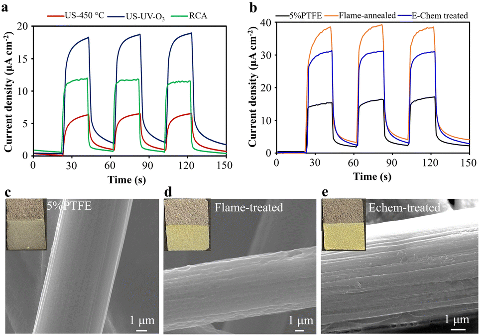 | ||
| Fig. 2 Photocurrent responses of the g-C3N4/WO3 heterojunction thin film deposited on pristine and pre-treated (a) FTO substrates, (b) carbon paper (CP) electrodes in 0.1 M KOH + 10% TEOA under 100 mW cm−2 (one sun) irradiation, SEM images of the (c) 5% PTFE coated CP, (d) flame-annealed CP, and (e) Echem-treated CP (insets: photographs of g-C3N4/WO3 thin film deposited on respective CP electrodes). | ||
Next, we pre-treated 5% PTFE-treated carbon paper (CP) electrodes (Toray, Fuel Cell Store) using two methods: (i) butane gas flame annealing and (ii) electrochemical treatment via chronopotentiometry (see Experimental for details). Fig. 2c–e shows the SEM images of 5% PTFE CP before and after pre-treatments. The pristine CP (Fig. 2c) exhibits a smooth surface, which develops uniform grooves and increased roughness after flame annealing (Fig. 2d). In contrast, electrochemical pre-treatment introduces distinct line defects (Fig. 2e). Using these pre-treated CP electrodes, we coated g-C3N4/WO3 thin films via EPD under the same conditions applied to FTO electrodes. Compared to the pristine CP (inset of Fig. 2c), the pre-treated CP electrodes exhibited significantly improved coating quality (insets of Fig. 2d and e). The low-magnification SEM image of the g-C3N4/WO3 thin film coated on flame-annealed CP (Fig. 1j) shows a uniform coating with a granular structure. The high-magnification SEM image (Fig. 1k) clearly shows the interconnected g-C3N4 and WO3 nanostructures, which appear as areas of lower and higher contrast, respectively, wrapping around the carbon fibres of the CP.
During the photocurrent measurements of these electrodes, the flame-annealed CP exhibited a 36 μA cm−2 at 1.23 V vs. RHE (Fig. 2b), which is 2.6 and 1.3 times higher than untreated PTFE-coated CP (13.8 μA cm−2) and electrochemically treated CP (27.7 μA cm−2), respectively. Based on these results, we recommend flame-annealed CP for achieving better EPD coatings and enhanced PEC activity. Interestingly, the photocurrent response of g-C3N4/WO3 thin film on CP was higher than on FTO, leading us to prefer CP electrodes for further optimisation. The flame-annealing effectively removes the 5% PTFE coating from commercial CP electrodes, rendering the surface more hydrophilic (Fig. S6, ESI†). This makes flame-annealed CP particularly advantageous for reactions requiring effective proton or water adsorption, such as hydrogen production from water splitting. However, for CO2 reduction reactions in aqueous electrolytes, a hydrophobic surface is essential to suppress parasitic hydrogen production and improve selectivity for CO2 reduction products. Therefore, the choice of electrode surface properties should be tailored to the target reaction.
| CH3COCH3 ⇌ CH3C(OH)CH2 | (1) |
| CH3C(OH)CH2 + I2 → CH3COCH2I + H+ + I− | (2) |
The g-C3N4/WO3 thin film deposited from the acetone + I2 suspension shows a photocurrent density of 36 μA cm−2 (Fig. 3a), while films prepared using water + I2 and IPA + I2 suspensions exhibited negligible changes in the photocurrent response. Based on these results, we highly recommend using acetone with I2 as a charging agent for suspension preparation. These findings highlight the importance of solvent selection and the role of charging agents in preparing effective suspensions for EPD processes. Furthermore, we demonstrated that reducing the particle size of g-C3N4/WO3 powder through ball milling does not improve the suspension quality in acetone and hence has no impact on the resulting EPD coating and photocurrent response (Fig. 3b).
 | ||
| Fig. 3 Photocurrent responses of the g-C3N4/WO3 thin films EPD coated from (a) water, IPA and acetone suspensions prepared in the presence of I2, (b) suspension prepared from as synthesised and balled milled g-C3N4/WO3 powders, (c) various suspension concentrations ranging from 0.5 to 5 mg mL−1, and (d) suspension prepared using one and two step ultrasonication process. All EPD coating was performed at 60 V for 1 minute. | ||
Using the optimum suspension concentration, we then studied the effect of ultrasonication time by varying it from 1 to 3 hours, adding I2 at the end, followed by an additional minute of ultrasonication. No significant differences were observed in the quality of EPD coatings and photocurrent responses for films deposited from suspensions prepared under these conditions (Fig. S9, ESI†). However, extending ultrasonication with I2 to 1 hour significantly improved the photocurrent of the g-C3N4/WO3 thin film from 25.7 μA cm−2 to 36 μA cm−2 at 1.23 V vs. RHE (Fig. 3d). This indicates that the reaction of I2 is slow, requiring an extended ultrasonication to generate sufficient positive charges on the particle surface for efficient EPD coating and enhanced PEC activity. Based on these findings, we recommend the following: (i) prepare the photocatalyst suspension in acetone with I2 as a charging agent, (ii) use a suspension concentration of 3 mg mL−1, and (iii) adopt a two-step ultrasonication process – ultrasonicate the photocatalyst powder for 1 hour, then add I2 and continue ultrasonication for an additional hour.
Controlling semiconductor film thickness is essential for optimising adhesion, uniformity, and PEC performance. To study this, we varied the deposition time for g-C3N4/WO3 films from 5 minutes to 6 seconds while maintaining deposition voltage at 60 V. The film thickness visibly differed across deposition times (Fig. S11, ESI†), and the semiconductor loading increased linearly at a rate of 0.014 mg cm−2 s−1 (Fig. 4a). The maximum loading of 4.203 mg cm−2 was obtained at 5 minutes, while the minimum of 0.043 mg cm−2 corresponded to 6 seconds (Table S9, ESI†). Photocurrent measurements revealed an optimal deposition time of 10 seconds, yielding the highest photocurrent density of 200 μA cm−2. This optimum value arises from a balance between charge carrier dynamics and light absorption: excessively thick films cause severe recombination of photogenerated charge carriers, while too-thin films fail to absorb sufficient light. A 10-second deposition forms a film with ideal parameters for visible light absorption (penetration range 50–400 nm in carbon nitride films)16 and efficient charge extraction to the surface.
 | ||
| Fig. 4 (a) The amount of g-C3N4/WO3 material deposited while varying EPD deposition time and photocurrent responses of the g-C3N4/WO3 thin film coated using EPD under various deposition times ranging from 300 to 6 seconds, (b) Nyquist plots of g-C3N4, WO3 and g-C3N4/WO3 hybrid materials obtained in 0.5 M KHCO3 electrolyte at a constant potential of 1.5 V vs. Ag/AgCl within the frequency range from 100 kHz to 1 Hz. (c) Stability test: photocurrent responses of g-C3N4/WO3/CP photoanode obtained in 0.1 M KOH solution containing 10% TEOA as a hole scavenger, (d) possible mechanism of photogenerated charge-carrier separation at the g-C3N4/WO3 heterojunction interface, (ϕWO3, ϕC3N4, X, VB, CB, EF, O to R and R to O represents work function of WO3, work function of g-C3N4, electron affinity, valence band, conduction band, Fermi-level, reduction reaction, and oxidation reaction, respectively), (e) workflow of optimised EPD parameters for coating g-C3N4/WO3 hybrid material thin films. | ||
Furthermore, we examined the effective charge separation at the g-C3N4/WO3 heterojunction interface using electrochemical impedance spectroscopy. The Nyquist plots of g-C3N4 and WO3 exhibit similar large semicircles, indicating poor charge transfer. In contrast, the g-C3N4/WO3 hybrid material shows a smaller semicircle, suggesting that the n–n heterojunction formed at the interface significantly enhanced the charge transfer (Fig. 4b). We also measured the open circuit voltage (OCV) of the g-C3N4/WO3 photoanode to validate the charge transfer at the heterojunction. The OCV of the photoanode increased from 0.11 V in the dark to 0.31 V under irradiation (Fig. S12, ESI†). This positive shift indicates the successful extraction of photogenerated electrons towards the substrate and holes towards the electrolyte.
3.3. Statistical analysis
We conducted a one-way ANOVA to determine the statistical significance of five independent variables—substrate pre-treatment, suspension solvent, suspension concentration, deposition time, and post-annealing temperature—on the photocurrent density. The results shown in Table S10 (ESI†) indicate that all five conditions significantly influenced the photocurrent density, as evidenced by their P-values, which were all well below the standard significance threshold of 0.05. The effect sizes (η2) for all these parameters were close to 1.0, suggesting a very strong effect of these factors on photoanode performance. However, the highest F-value observed for deposition time (F = 18259.70), followed by post-annealing temperature (F = 17262.96), suggests that these two variables had the strongest influence on the overall photocurrent density.
3.4. Stability and reproducibility
The stability test of the g-C3N4/WO3 thin film on CP is crucial to ensure consistent photocurrent response and stability over multiple cycles, thereby validating the material's reliability for practical applications. Hence, we repeated the photocurrent measurements of the optimised C3N4/WO3/CP electrode three times every other day for a week and observed no significant change (Fig. 4c). This suggests that the present EPD-coated g-C3N4/WO3 thin film is highly stable for long-term operation. It is worth mentioning that after each measurement, the electrode was washed with deionized (DI) water, dried in air at 100 °C for 2 hours, and stored in an airtight container. Furthermore, we tested the reproducibility of the EPD coating by depositing g-C3N4/WO3 thin film on three CP supports. The photocurrent responses of these three different photoanodes were 99% identical (Fig. S14, ESI†), suggesting that coating the photocatalyst film using the present optimised EPD workflow is highly reproducible. Additionally, we prepared the separate g-C3N4/CP and WO3/CP photoanodes and observed their photocurrent densities of 50 μA cm−2 and 80 μA cm−2, respectively (Fig. S15, ESI†), which are 4 and 2.5 times less than the PEC activity of the g-C3N4/WO3/CP heterojunction photoanode (200 μA cm−2). It strongly suggests that the n–n heterojunction constructed at the interface between g-C3N4 and WO3 within the EPD-deposited film separates the photogenerated charge carriers efficiently through the Z-scheme mechanism (Fig. 4d).The PEC activity of the present g-C3N4/WO3/CP heterojunction photoanode at 1.23 V vs. RHE is higher than the state-of-the-art g-C3N4-based thin film prepared from its suspension using EPD (Table S11, ESI†). Additionally, we compared our EPD-coated g-C3N4/WO3/CP photoanode performance with those obtained using other methods, such as thermal vapour condensation, direct growth, microcontact-printing, solvothermal, electrospinning, liquid-based growth, doctor-blade, and seed-growth (Table S12, ESI†). It is evident that our EPD recipe not only shows high photocurrent but also stands out for its simplicity, low cost, ability to form uniform coatings, ease of thickness control, and suitability for large-area and complex substrate geometries.
4. Conclusions
We have developed a comprehensive strategy to maximise the functional properties of carbon nitride in the photoanode (Fig. 4e). It involves (i) the use of flame-annealed CP electrodes, (ii) preparing a suspension in acetone with I2 as a charging agent, (iii) maintaining suspension concentration at the optimum 3 mg mL−1, (iv) employing a two-step ultrasonication process, (v) using a deposition voltage of 60 V and a 10-second deposition under stirring, and (vi) conducting post-annealing at 300 °C. This optimised EPD workflow leads to the highly effective formation of g-C3N4/WO3 hybrid thin films on CP electrodes and achieves the record photocurrent density of 0.2 mA cm−2 at 1.23 V vs. RHE with exceptional stability and reproducibility. The most important parameter is the thickness and uniformity of the film, which are controlled by the deposition time and voltage. Furthermore, we clarified the Z-scheme mechanism responsible for the photocurrent enhancement in the well-constructed g-C3N4/WO3 heterojunction hybrid material, supported by XPS, HR-TEM, and EIS analysis. These findings highlight the potential of the present optimised EPD workflow technique for fabricating large-scale photoelectrodes to be used in energy conversion applications.Author contributions
M. T. developed the methodology, and performed SEM imaging, electrochemical and photoelectrochemical characterization studies, analysed and interpreted the results, and wrote the manuscript. S. L. and M. M. synthesised the materials and performed part of the photocurrent measurements. T. M. L. performed HRTEM imaging, XRD, and UV-vis measurements. E. C. K. performed and interpreted the XPS results. M. T., A. N. K., and J. A. F. supervised the project and reviewed and edited the manuscript.Data availability
The data supporting the findings of this study are available within the article and its ESI.† Additional datasets generated during this study, including raw and processed data, are available from the corresponding author upon reasonable request.Conflicts of interest
The authors declare no conflicts.Acknowledgements
The authors acknowledge financial support from the Engineering and Physical Sciences Research Council (EPSRC), project Metal Atoms on Surfaces and Interfaces (MASI) for Sustainable Future (EP/V000055/1).Notes and references
- D. B. Hernández-Uresti, A. Vázquez, S. Obregón and M. A. Ruíz-Gómez, Mater. Lett., 2017, 200, 59–62 CrossRef.
- M. Ghaemmaghami, Y. Yamini, H. Amanzadeh and B. Hosseini Monjezi, Chem. Commun., 2018, 54, 507–510 RSC.
- J. Xu and M. Shalom, ACS Appl. Mater. Interfaces, 2016, 8, 13058–13063 CrossRef CAS PubMed.
- Y. J. Seo, P. K. Das, M. Arunachalam, K.-S. Ahn, J.-S. Ha and S. H. Kang, Int. J. Hydrogen Energy, 2020, 45, 22567–22575 CrossRef CAS.
- P. Wongchaiya, T. K. N. Nguyen, P. Sujaridworakun, S. Larpkiattaworn, T. S. Suzuki and T. Uchikoshi, Adv. Powder Technol., 2024, 35, 104460 CrossRef CAS.
- Y. Wei, Z. Wang, J. Su and L. Guo, ChemElectroChem, 2018, 5, 2734–2737 CrossRef CAS.
- M. Zhao, X. Yang, X. Li, Z. Tang and Z. Song, J. Electroanal. Chem., 2021, 893, 115324 CrossRef CAS.
- T. M. LeMercier, M. Thangamuthu, E. C. Kohlrausch, Y. Chen, C. T. Stoppiello, M. W. Fay, G. A. Rance, G. N. Aliev, W. Theis, J. Biskupek, U. Kaiser, A. E. Lanterna, J. A. Fernandes and A. N. Khlobystov, Sustainable Energy Fuels, 2024, 8, 1691–1703 RSC.
- M. Thangamuthu, K. Vankayala, L. Xiong, S. Conroy, X. Zhang and J. Tang, ACS Catal., 2023, 13, 9113–9124 CrossRef CAS PubMed.
- Y. Ge, X. Guo, D. Zhou and J. Liu, Nanoscale, 2022, 14, 12358–12376 RSC.
- C. Fan, J. Miao, G. Xu, J. Liu, J. Lv and Y. Wu, RSC Adv., 2017, 7, 37185–37193 RSC.
- A. K. Nayak, S. Lee, Y. I. Choi, H. J. Yoon, Y. Sohn and D. Pradhan, ACS Sustainable Chem. Eng., 2017, 5, 2741–2750 CrossRef CAS.
- X. Zhu, H. Deng and G. Cheng, Inorg. Chem. Commun., 2021, 132, 108814 CrossRef CAS.
- Y. Shang, C. Wang, C. Yan, F. Jing, M. Roostaeinia, Y. Wang, G. Chen and C. Lv, J. Colloid Interface Sci., 2023, 634, 195–208 CrossRef CAS PubMed.
- L. Grinis, S. Dor, A. Ofir and A. Zaban, J. Photochem. Photobiol., A, 2008, 198, 52–59 CrossRef CAS.
- J. Zhang, M. Zhang, R. Sun and X. Wang, Angew. Chem., 2012, 124, 10292–10296 CrossRef.
- A. K. Mohamedkhair, Q. A. Drmosh, M. Qamar and Z. H. Yamani, Catalysts, 2021, 11, 1–16 CrossRef.
Footnote |
| † Electronic supplementary information (ESI) available. See DOI: https://doi.org/10.1039/d5ma00301f |
| This journal is © The Royal Society of Chemistry 2025 |